Note: Descriptions are shown in the official language in which they were submitted.
CA 02553137 1996-08-20
-1-
ELECTRONICALLY ADDRESSABLE MICROENCAPSULATED INK
AND DISPLAY THEREOF
Background
Currently, printing of conductors and resistors is well known
in the art of circuit board manufacture. In order to incorporate
logic elements the standard practice is to surface mount
semiconductor chips onto said circuit board. To date there does
not exist a system for directly printing said logic elements onto
an arbitrary substrate.
In the area of flat panel display drivers there exists
technology for laying down logic elements onto glass by means of
vacuum depositing silicon or other semiconductive material and
subsequently etching circuits and logic elements. Such a
technology is not amenable to laying down logic elements onto
arbitrary surface due to the presence of the vacuum requirement and
the etch step.
In the area of electronically addressable contrast media as
may be used to effect a flat panel display emissive and reflective
electronically active films such as electroluminscent and
electrochromic films, polymer dispersed liquid crystal films, and
bichromal microsphere elastomeric slabs are known. No such
directly electronically addressable contrast media however is
amenable to printing onto an arbitrary surface.
Finally in the area of surface actuators electrostatic motors
which may be etched or non-etched are known in the art. In the
first case such etched devices suffer from their inability to be
fabricated on arbitrary surfaces. In the second case, non-etched
devices suffer from the inability to incorporate drive logic and
electronic control directly onto the actuating surface.
It is therefore desirable to overcome the limitations of the
prior art in the area of printable logic, display and actuation.
CA 02553137 1996-08-20
-2-
Summary of the Invention
In accordance with one aspect of the invention, there is
provided a method of making a microencapsulated electrically
addressable contrast media ink, comprising the steps of: providing
a layer of an uncured material, the material being curable by
ultraviolet radiation; disposing a photo-mask over the uncured
material, the photo-mask exposing selected portions of the uncured
material; forming a cellular structure by applying ultraviolet
radiation to cure the exposed uncured material; and
filling the cellular structure formed by the cured material with an
internal phase.
In accordance with another aspect of the invention, there is
provided an electrically addressable ink comprising a microcapsule,
the microcapsule comprising: a first particle having a first
charge; and a second particle having a second charge; wherein
applying an electric field having a first polarity to the
microcapsule effects a perceived color change by causing one of the
first and second articles to migrate in a direction responsive to
the field.
In accordance with another aspect of the inven~ion, there is
provided a microencapsulated ink system, comprising a microcapsule.
The microcapsule comprises a photoconductive semiconductor
particle; and a dye indicator particle; wherein the application of
an electric field to the microcapsule causes the photoconductive
semiconductor particle to generate free charge, causing the dye
indicator to effect a first color state.
In accordance with another aspect of the invention, there is
provided an electrically addressable ink comprising a microcapsule.
The microcapsule comprises a hairpin-shaped molecule having a first
portion and a second portion, the hair-pin shaped molecule
comprising: a first moiety having a first charge attached to the
first portion of the hairpin-shaped molecule; and a second moiety
having a second charge attached to the second portion of the
hairpin-shaped molecule, the second moiety capable of reacting with
the first moiety, the second charge being opposite to the first
CA 02553137 1996-08-20
-3-
charge; the reaction between the first moiety and the second moiety
defining a closed state of the hairpin-shaped molecule effecting a
first color state; and the separation of the first moiety from the
second moiety defining an open state of the hairpin-shaped
molecule, effecting a second color state.
In accordance with another aspect of the invention, there is
provided an electronically addressable ink comprising a
microcapsule. The microcapsule comprises a polymer molecule having
a first non-linear shape in the presence of a first electric field,
the polymer molecule comprising: a first moiety attached to a first
location; and a second moiety attached to a second location;
wherein the application of a second electric field causes the
polymer molecule to assume a linear shape, separating the first and
second moieties to effect a first color state.
In accordance with another aspect of the invention, there is
provided an electrically addressable medium comprising a
microcapsule, the microcapsule further comprising a non-colored dye
solvent complex, the dye solvent complex being stable when no
electric field is applied and wherein applying an electric field
causes the dye solvent complex to separate into a dye complex and a
solvent complex, effecting a first color state.
In accordance with another aspect of the invention, there is
provided a method for fabricating a display, comprising the steps
of: dispersing a semiconductive material in a binder to form an
electrically active ink; providing the electrically active ink to a
fluid delivery system; and printing the electrically active ink to
a substrate via the fluid delivery system.
In accordance with another aspect of the invention, there is
provided a method for depositing electrically addressable contrast
media onto a substrate comprising the steps of: disposing adjacent
the substrate a microcapsule containing an electrically addressable
contrast media to be deposited; and directing a light source so
that it impinges on the microcapsule causing the microcapsule to
burst and deposit the electrically active contrast media onto the
surface of the substrate.
CA 02553137 1996-08-20
-4-
In accordance with another aspect of the invention, there is
provided a method for printing a display, comprising the steps of:
dispersing an electrically active material in a binder to form an
electrically active ink; providing a first movable jet depositing
the electrically active ink onto a substrate; reducing the
electrically active ink on the substrate to form a trace on the
substrate.
In accordance with another aspect of the invention, there is
provided a microencapsulated contrast media system comprising a
plurality of individual cells, at least one of the plurality of
individual cells filled with an electronically addressable contrast
media, wherein the contrast media comprises a polymer-building
block or a cross-linking agent adapted to form a solid layer at an
interface of the contrast media.
In accordance with another aspect of the invention, there is
provided a microencapsulated contrast media system comprising a
plurality of individual cells, at least one of the plurality of
individual cells filled with an electronically addressable contrast
media dispersed in a dielectric solvent, wherein the dielectric
solvent is adapted to facilitate bistability of the contrast media.
In accordance with another aspect of the invention, there is
provided an electrophoretic display comprising a plurality of
individual cells, at least one of the plurality of individual cells
filled with an electronically addressable contrast media, wherein
the contrast media comprises a polymer-building block or a cross-
linking agent adapted to form a solid layer at an interface of the
contrast media.
In accordance with another aspect of the invention, there is
provided an electrophoretic display comprising a plurality of
individual cells, at least one of the plurality of individual cells
filled with an electronically addressable contrast media dispersed
in a dielectric solvent, wherein the dielectric solvent is adapted
to facilitate bistability of the contrast media.
In accordance with another aspect of the invention, there is
provided a method for the manufacture of an electrophoretic display
comprising the steps of: providing a radiation-curable substrate;
CA 02553137 1996-08-20
-5-
imagewise exposing the radiation-curable substrate to a radiation
source thereby forming a plurality of individual cells in the
radiation-curable substrate; and filling at least one of the
plurality of individual cells with an electrophoretic contrast
media, the contrast media comprising a polymer-building block or a
cross-linking agent.
In accordance with another aspect of the invention, there is
provided a method for manufacturing an electrophoretic display
comprising the steps of: providing a liquid suspension, comprising
a first species of electrophoretic particles having a first optical
property and a means of forming a solid layer; providing a
substrate; distributing the liquid suspension onto the substrate;
and forming a solid layer on the substrate by exposing the liquid
suspension to a stimulus, wherein the solid layer comprises at
least part of a cellular structure.
In accordance with another aspect of the invention, there is
provided an electronically active ink comprising a
microencapsulated system having an optical reflectance modulatable
by means of application of an electric field.
In accordance with another aspect of the invention, there is
provided a system for producing a particle with an implanted dipole
and more than one optical property, comprising: a first electrode
imparting a first charge having a first polarity to a first
material having a first optical property; a second electrode
imparting a second charge having a second polarity to a second
material having a second optical property; and a combiner
electrostatically combining the first and second charged materials
into a particle with an implanted dipole.
The system may further comprise a first nozzle producing
atomized droplets of the first material, the droplets having a
charge of the first polarity and the first optical property; and a
second nozzle producing atomized droplets of the second material,
the droplets having a charge of the second polarity and the second
optical property; wherein the first nozzle and the second nozzle
are disposed such that the droplets of the first and second charged
CA 02553137 1996-08-20
-6-
materials combine electrostatically to form a particle having an
implanted dipole.
In accordance with another aspect of the inven~ion, there is
provided a method for producing a particle having an implanted
dipole and more than one optical property, comprising the steps of:
providing a first material having a first optical property and a
charge of a first polarity to a first atomizing nozzle; providing a
second material having a second optical property and a charge of a
second polarity to a second atomizing nozzle; atomizing the first
material into droplets emitted by the first nozzle; atomizing the
second material into droplets emitted by the second nozzle; and
arranging the first and second nozzles so that the emitted droplets
of the first and second materials combine electrostatically to form
a particle having an implanted dipole.
In accordance with another aspect of the invention, there is
provided a method for producing a particle with an implanted dipole
and more than one optical property, comprising the steps of:
imparting a first charge of a first polarity to a first material
having a first optical property; imparting a second charge of a
second polarity to a second material having a second optical
property; and combining the first and second materials
electrostatically into a particle having an implanted dipole.
There is disclosed herein a system of electronically active
inks and means for printing said inks in an arbitrary pattern onto
a large class of substrates without the requirements of standard
vacuum processing or etching. Said inks may incorporate
mechanical, electrical or other properties and may provide but are
not limited to the following function: conducting, insulating,
resistive, magnetic, semiconductive, light modulating,
piezoelectric, spin, optoelectronic or thermoelectric.
In one embodiment this invention provides for a
microencapsulated electric field actuated contrast ink system
suitable for addressing by means of top and bottom electrodes or
solely bottom electrodes and which operates by means of a bichromal
dipolar microsphere, electrophoretic, dye system, liquid crystal,
electroluminescent dye system or dielectrophoretic effect. Such an
CA 02553137 1996-08-20
ink system may be useful in fabricating an electronically
addressable display on any of a large class of substrate materials
which my be thin, flexible and may result in an inexpensive
display.
In another embodiment this invention provides for a
semiconductive ink system in which a semiconductor material is
deployed in a binder such that when said binder is cured a
percolated structure with semiconductive properties results.
In another embodiment this invention provides for systems
capable of printing an arbitrary pattern of metal or semiconductive
materials by means of photoreduction of a salt, electron beam
reduction of a salt, jet electroplating, dual jet electroless
plating or inert gas or local vacuum thermal, sputtering or
electron beam deposition.
In another embodiment this invention provides for
semiconductor logic elements and electro-optical elements which may
include diode, transistor, light emitting, light sensing or solar
cell elements which are fabricated by means of a printing process
or which employ an electronically active ink system as described in
the aforementioned embodiments. Additionally said elements may be
multilayered and may form multilayer logic including vias and three
dimensional interconnects.
In another embodiment this invention provides for an
electronically addressable display in which some or all of address
lines, electronically addressable contrast media, logic or power
are fabricated by means of a printing process or which employ an
electronically active ink system as described in the aforementioned
embodiments.
In another embodiment this invention provides for an
electrostatic actuator or motor which may be in the form of a clock
or watch in which some or all of address lines, logic or power are
fabricated by means of a printing process or which employ an
electronically active ink system as described in the aforementioned
embodiments.
CA 02553137 1996-08-20
_g_
In another embodiment this invention provides for a
wrist watch band which includes an electronically
addressable display in which some or all of address lines,
electronically addressable contrast media, logic or power
are fabricated by means of a printing process or which
employ an electronically active ink system as described in
the aforementioned embodiments.
In another embodiment this invention provides for a
spin computer in which some or all of address lines,
electronically addressable spin media, logic or power are
fabricated by means of a printing process or which employ
an electronically. active ink system as described in the
aforementioned embodiments.
Further features and aspects will become apparent
from the following description and from the claims.
Brief Description of the Drawings
The foregoing and other objects, features and
advantages of the invention will be apparent from the
following more particular description of preferred
embodiments of the invention, as illustrated in the
accompanying drawings in which like reference characters
refer to the same parts throughout the different views.
The drawings are not necessarily to scale, emphasis
instead being placed upon illustrating the principles of
the invention.
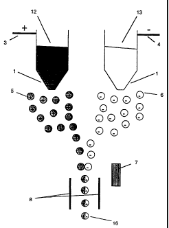
Figures lA-F are schematic representations of means
of fabricating particles with a permanent dipole moment.
Figures 2A-C are schematic representations of means
o-~ microencapsulation.
Figures 3A-E are schematic representations of
microencapsulated electronically addressable contrast
media systems suitable for top to bottom addressing.
CA 02553137 1996-08-20
-9-
Figure 4A-M are schematic representations of
microencapsulated electronically addressable contrast
media systems suitable for bottom addressing.
Figures 5A-D are schematic representations of
microencapsulated electronically addressable contrast
media systems based on a dielectrophoretic effect.
Figures 6A-B are schematic representations of
microencapsulated electronically addressable contrast
media systems based on a frequency dependent
dielectrophoretic effect.
Figures 6C-E are plots of the dielectric parameter as
a function of frequency for various physical systems.
Figures 7A-D are schematic representations of
electronic ink systems and means for printing the same.
Figure 8 is a schematic representation of a laser
reduced metal salt ink system.
Figures 9A-E are schematic representations of
electronic ink systems and means for printing the same.
Figures l0A-D are schematic diagrams of printed
transistor structures.
Figure 11 is a schematic diagram of an electronic
display employing printed elements.
Figure 12 is a schematic diagram of an electrostatic
motor which may be in the form of a watch or clock in
which said electrostatic elements are printed
Figure 13 is a schematic diagram of a watch in which
the wristband of said watch incorporates an electronically
addressable display having printed elements.
Figure 14 is a schematic diagram of a spin computer.
Detailed Description of a Preferred Embodiment
Means are known in the prior art for producing
CA 02553137 1996-08-20
-10-
bichromal particles or microspheres for use in electronic
displays. Such techniques produce a particle that does
not have an implanted dipole moment but rather relies in
general on the Zeta potential of the material to create a
permanent dipole. Such a scheme suffers from the fact
that it links the material properties to the electronic
properties thus limiting the size of the dipole moment
which may be created. Figure 1 details means of producing
particles, either bichromal as might be used in an
l0 electrostatic display, or monochromal as might be used in
a dielectrophoretic display, with an implanted dipole
moment.
Referring to Figure 1 A atomizing nozzles 1 are
loaded with materials 12 and 13 which may be
differentially colored. A first atomizing nozzle may be
held at a positive potential 3 and a second nozzle may be
held at a negative potential 4. Such potentials aid in
atomization and impart a charge to droplets which form
from said nozzles producing positively charge droplets 5
and negatively charged droplets 6. Such opposite charged
droplets are attracted to each other electrostatically
forming an overall neutral pair. After the formation of a
neutral particle there is no more electrostatic attraction
and no additional droplets are attracted to the neutral
pair. If said material 12 and 13 are such that they are
liquid when exiting said nozzles and either cool to form a
solid or undergo a chemical reaction which may involve an
additional hardening agent to form a solid then said
charge may be trapped on each side of said neutral pair
forming a bichromal solid particle with an implanted
dipole 16. By suitable choice of materials such as
polyethylene, polyvinalydene fluoride or other materials
such metastable dipoles may persist for long periods of
CA 02553137 1996-08-20
-11-
time as is known in the art of electrets. A heating element 7 may serve to
reheat said
pair thus minimizing surface tension energy and serving to reform said pair
into a more
perfect spherical shape. Finally a set of electrodes 8 biased at either the
same or
opposite voltage may be employed to trap particles which are not overall
charge
neutral.
Referring to Figure 1B a similar apparatus may be employed to create a
monochromal particle with an implanted dipole. In this arrangement nozzles
containing material of the same color 12 are employed as before to create a
monochromal particle with implanted dipole 21.
Referring to Figure 1 C and 1 D alternative means are shown for producing a
bichromal particle with implanted dipole by means of combining two
differentially
colored materials 12 and 13 on a spinning disk 11 or in a double barreled
nozzle 19.
Said materials are charged by means of positive electrode 14 and negative
electrode 15
and combine by means of electrostatic attraction at the rim of said disk or
exit of said
double barrel nozzle to form bichromal particle with implanted dipole moment
16.
Said means differs from that known in the art by means of causing said two
different
materials 12 and 13 to coalesce by means of electrostatic attraction as
opposed to
relying on surface properties and interactions between the two materials.
Additionally
the present scheme creates a particle with an implanted dipole moment 16 which
may
serve to create a larger dipole moment than that possible from the naturally
occurring
Zeta potential.
Referring to Figure 1 E and 1 F a similar apparatus may be employed to
create'a
monochromal particle with an implanted dipole. In this arrangement nozzles
containing material of the same color 12 are employed as before to
CA 02553137 1996-08-20
-12-
create a monochromal particle with implanted dipole 21.
A large number of techniques are known in the
literature for microencapsulating one material inside of
another material. Such techniques are generally used in
the paper or pharmaceutical industry and do not generally
produce a microcapsule which embodies simultaneously the
properties of optical clarity, high dielectric strength,
impermeability and resistance to pressure. With proper
modification however these techniques may be made amenable
to microencapsulating systems with electronic properties.
Referring to Figure 2A an internal phase 25 which may
be a liquid or may be a solid with an additional
associated surface layer 27. Said internal phase if
liquid or said associated surface layer may contain a
polymer building block, such as Adipoyl Chloride ~in
Silicone Oil. Said internal phase, with associated
boundary layer in the case of a liquid, may then be
dispersed in a continuous phase liquid 30 which may be an
aqueous solution which is immiscible with said internal
phase or associated surface layer. Finally a solution 40
may be added which contains another polymer building block
or cross linking agent may be added to continuous phase
liquid 30. Said solution 40 has the effect of forming a
solid layer at the interface of the internal phase or
associated surface layer and said continuous phase liquid
thus acting to microencapsulate said internal phase.
Referring to Figure 2B an internal phase 25 which may
be a solid or a liquid may be caused to pass through a
series of liquid films 50,60,70 which may contain polymer
30 building blocks, cross linking agents and overcoat
materials such that a final microcapsule 120 results
comprised of an internal phase 25, an associated surface
layer 27 and an outer shell 80.
CA 02553137 1996-08-20
-13-
An alternate means of microencapsulation is shown in
Figure 2C. In this scheme a light source 82 which may be
a W light source passes in some areas through a photomask
84 exposing a crosslinkable polymer which may be caused to
form a cellular structure 86. The individual cells of
said cellular structure may then be filled with an
internal phase 25.
Employing the systems described in Figures 2A-C it is
possible to microencapsulate systems with electronically
active properties specifically electronically addressable
contrast media. Figure 3 details such electronically
addressable contrast media systems which are suitable for
addressing by means of a top clear electrode 100 and
bottom electrode 110. Referring to Figure 3A a
microcapsule 120 may contain a microsphere with a
positively charged hemisphere 142 and a negatively charged
140 hemisphere and an associated surface layer material
130. If said hemispheres are differentially colored an
electric field applied to said electrodes may act to
change the orientation of said sphere thus causing a
perceived change in color.
Referring to Figure 3B a microcapsule 120 may contain
positively charged particles of one color 210 and
negatively charged particles of another color 220 such
that application of an electric field to said electrodes
causes a migration of the one color or the other color,
depending on the polarity of the field, toward the surface
of said microcapsule and thus effecting a perceived color
change. Such a system constitutes a microencapsulated
e-lectrophoretic system.
Referring to Figures 3C-D a microcapsule 120 may
contain a dye, dye precursor or dye indicator material of
a given charge polarity 230 or a dye, dye precursor or dye
CA 02553137 1996-08-20
-14-
indicator material attached to a particle of given charge polarity such as a
microsphere
with an appropriate surface group attached and a reducing, oxidizing, proton
donating,
proton absorbing or solvent agent attached to a particle of the other charge
polarity.
Under application of an electric field said dye substance 230 is maintained
distal to said
reducing, oxidizing, proton donating, proton absorbing or solvent agent 240
thus
effecting one color state as in Figure 3C. Upon deapplication of said electric
field said
dye substance and said reducing, oxidizing, proton donating, proton absorbing
or
solvent agent may bond to form a complex 245 of second color state. Suitable
materials for use in this system are leuco and lactone dye systems and other
ring
structures which may go from a state of one color to a state of a second color
upon
application of a reducing, oxidizing or solvent agent or dye indicator systems
which
may go from a state of one color to a state of a second color upon application
of a
proton donating or proton absorbing agent as is lrnown in the art. An
additional gel or
polymer material may be added to the contents of said microcapsule in order to
effect a
bistability of the system such that said constituents are relatively immobile
except on
application of an electric field.
Referring to Figure 3E a microcapsule 120 may contain phosphor particle 255
and photoconductive semiconductor particles and dye indicator particles 260 in
a
suitable binder 250. Applying an AC electric field to electrodes 100 and 110
causes
AC electroluminescence which causes free charge to be generated in the
semiconducting material further causing said dye indicator to c~ange color
state.
CA 02553137 1996-08-20
-15-
Referring to Figures 4A-M it may be desirable to develop ink systems which are
suitable for use without a top transparent electrode 100 which may degrade the
optical
characteristics of the device. Referring to Figures 4A and 4B the chemistry as
described in reference to Figures 3C-D may be employed with in-plane
electrodes such
that said chemistry undergoes a color switch from one color state to a second
color state
upon application of an electric field to in-plane electrodes 270 and 280. Such
a system
is viewed from above and thus said electrodes may be opaque and do not effect
the
optical characteristics of said display.
As another system in-plane switching techniques have been employed in
transmissive LCD displays for another purpose, namely to increase viewing
angle of
such displays. Referring to Figures 4C and 4D a bistable liquid crystal system
of the
type demonstrated by Hatano et. al. of Minolta Corp. is modified to be
effected by in-
plane electrodes such that a liquid crystal mixture transforms from a first
transparent
planar structure 290 to a second scattering focal conic structure 292.
Referring to Figure 4E the system of Figure 3E may be switched by use of in-
plane electrodes 270 and 280.
Other systems may be created which cause a first color change by means of
applying an AC field and a second color change by means of application of
either a DC
field or an AC field of another frequency. Referring to Figures 4F-G a hairpin
shaped
molecule or spring in the closed state 284 may have attached to it a
positively charged
282 and a negatively charged 283 head which may be microspfi~eres with
implanted
dipoles. Additionally one side of said hairpin shaped molecule or spring has
attached to
it a leuco dye 286 and the other side of said
CA 02553137 1996-08-20
-16-
hairpin shaped molecule or spring has attached to it a reducing agent 285.
When said
molecule or spring is in the closed statg 284 then said leuco dye 286 and said
reducing
agent 285 are brought into proximity such that a bond is formed 287 and said
leuco dye
is effectively reduced thus effecting a first color state. Upon applying an AC
electric
field with frequency that is resonant with the vibrational mode of said
charged heads
cantilevered on said hairpin shaped molecule or spring said bond 287 may be
made to
break thus yielding an open state 288. In said open state the leuco dye and
reducing
agent are no longer proximal and the leuco dye, being in a non-reduced state,
effects a
second color state. The system may be reversed by applying a DC electric field
which
serves to reproximate the leuco dye and reducing agent groups. Many molecules
or
microfabricated structures may serve as the normally open hairpin shaped
molecule or
spring. These may include oleic acid like molecules 289. Reducing agents may
include sodium dithionite. We note that the system as discussed is bistable.
We note
also that energy may be stored in said hairpin shaped molecule or spring and
as such
said system may also function as a battery.
Referring to figures 4I-K an alternative leucodye-reducing agent system may
employ a polymer shown in Figure 4I in a natural state 293. When a DC electric
field
is applied said polymer assumes a linear shape 294 with leuco 286 and reducing
agent
285 groups distal from each other. Upon application of either a reversing DC
field or
an AC electric field said polymer will tend to coil bringing into random
contract said
leuco and reducing groups forming a bond 287 with a corres~oi~ding color
change.
Said polymer serves to make said system bistable.
CA 02553137 1996-08-20
-17-
Referring to Figures 4L and 4M a similar system is possible
but instead polymer leuco and reducing groups may be attached to
oppositely charged microspheres directly by means of a bridge 296
which may be a biotin-streptavidin bridge, polymer bridge or any
other suitable bridge. As before application of a DC field cause
leuco and reducing groups to become distal whereas application of a
reverse DC field or AC field brings into random contact the leuco
and reducing groups. A polymer may be added to aid in the
stability of the oxidized state.
Referring to Figures 5A-D and Figures 6A-B an entirely
different principle may be employed in an electronically
addressable contrast media ink. In these systems the
dielectrophoretic effect is employed in which a species of higher
dielectric constant may be caused to move to a region of high
electric field strength.
Referring to Figures 5A and 5B a non-colored dye solvent
complex 315 which is stable when no field is applied across
electrode pair 150 may be caused to become dissociate into colored
dye 300 and solvent 310 components by means of an electric field
170 acting differentially on the dielectric constant of said dye
complex and said solvent complex as applied by electrode pair 150.
It is understood that the chemistries as discussed in the system of
Figures 3C - D may readily be employed here and that said dye
complex and said solvent complex need not themselves have
substantially different dielectric constants but rather may be
associated with other molecules or particles such as microspheres
with substantially different dielectric constants. Finally it is
understood that a gel or polymer complex may be added to the
contents of said microcapsule in order to effect a bistability.
CA 02553137 1996-08-20
-18-
Referring to Figures 5C-D stacked electrode pairs 150
and 160 may be employed to effect a high electric field
region in a higher 170 or lower 180 plane thus causing a
higher dielectric constant material such as one hemisphere
of a bichromal microsphere 141 or one species of a mixture
of colored species 147 to migrate to a higher or lower
plane respectively and give the effect of differing color
states. In such schemes materials 165 which may be
dielectric materials or may be conducting materials may be
employed to shape said electric fields.
Referring to Figures 6A-B, systems based on a
frequency dependent dielectrophoretic effect are
described. Such systems are addressed by means of
applying a field of one frequency to produce a given color
and applying a field of a different frequency to produce
another color. Such a functionality allows for a rear
addressed display.
Referring to Figure 6A, a microcapsule 120
encompasses an internal phase 184 which may be a material
which has a frequency independent dielectric constant as
shown in Plot 6C, curve 320 and which may have a first
color B and material 182 which has a frequency dependent
dielectric constant and a second color W. Said.frequency
dependent material may further have a high dielectric
constant at low frequency and a smaller dielectric
constant at higher frequency as shown in Figure 6C 322.
Application of a low frequency AC field by means of
electrodes 270 and 280 causes said material 182 to be
attracted to the high field region proximal to the
electrodes thus causing said microcapsule to appear as the
color B when viewed from above. Conversely application of
a high frequency AC field by means of electrodes 270 and
280 causes said material 184 to be attracted to the high
CA 02553137 1996-08-20
-19-
field region proximal the electrodes thus displacing material 182
and thus causing said microcapsule to appear as the color W when
viewed from above. If B and W correspond to Black and White then a
black and white display may be effected. A polymer material may be
added to internal phase 184 to cause said system to be bistable in
the field off condition. Alternatively stiction to the internal
side wall of said capsule may cause bistability.
Referring to Figure 6A, material 182 and Figure 6C, this
patent teaches the fabrication of a particle with an engineered
frequency dependent dielectric constant. The means for fabricating
this particle are depicted in Figures 1B, E and F. At low
frequency such dipolar particles have sufficiently small mass that
they may rotate in phase with said AC field thus effectively
cancelling said field and acting as a high dielectric constant
material. At high frequency however the inertia of said particles
is such that they cannot keep in phase with said AC field and thus
fail to cancel said field and consequently have an effectively
small dielectric constant.
Alternatively material 182 may be comprised of naturally
occurring frequency dependent dielectric materials. Materials
which obey a frequency dependence functionality similar to the
artificially created dipole material discussed above and which
follow curves similar to Figure 6C, curve 322 include materials
such as Hevea rubber compound which has a dielectric constant of K
3 6
- 36 at f = 10 Hz and K = 9 at f = 10 Hz, materials with ohmic
loss as are known in Electromechanics of Particles by T.B. Jones
and macromolecules with permanent dipole moments.
Additionally material 182 may be a natural or artificial cell
material which has a dielectric constant frequency dependence as
depicted in Figure 6D, curve 330 as are discussed in
Electromechanics of Particles by T.B. Jones. Such particles are
further suitable for fabrication of an electronically addressable
contrast ink.
Referring to Figure 6B a system is depicted capable of
effecting a color display. Microcapsule 120 contains a particle of
CA 02553137 1996-08-20
-20-
a first dielectric constant, conductivity and color 186, a particle
of a second dielectric constant, conductivity and color and an
internal phase of a third dielectric constant, conductivity and
color 190. Referring to Plot 6E it is known in the art of
electromechanics of particles that for particles with ohmic loss
(e.g. finite conductivity) that at low frequency the DC
conductivity governs the dielectric constant whereas at high
frequency the dielectric polarization governs the dielectric
constant. Thus a particle with finite conductivity has a
dielectric constant K as a function of frequency f as in Plot 6E,
curve 338. A second particle of second color has a dielectric
constant K as a function of frequency f as in Figure 6E, curve 340.
Finally an internal phase with no conductivity has a frequency
independent dielectric constant K, curve 336. If an AC field of
frequency fl is applied by means of electrodes 270 and 280,
material 186 of color M will be attracted to the high field region
proximal to said electrodes thus causing said microcapsule to
appear as a mixture of the colors C and Y, due to the other
particle and internal phase respectively, when viewed from above.
If an AC field of frequency f2 is applied by means of electrodes
270 and 280 material 188 of color Y will be attracted to the high
CA 02553137 1996-08-20
-21-
proximal to said electrodes thus causing said microcapsule
to appear as a mixture of the colors C and M when viewed
from above. Finally if an AC field of frequency f3 is
applied by means of electrodes 270 and 280 internal phase
190 of color C will be attracted to the high field region
proximal to said electrodes thus causing said microcapsule
to appear as a mixture of the colors M and Y when viewed
from above. If C M and Y correspond to Cyan, Magenta and
Yellow a color display may be effected.
It is understood that many other combinations of
particles with frequency dependent dielectric constants
arising from the physical processes discussed above may be
employed to effect a frequency dependent electronically
addressable display.
In addition to the microencapsulated electronically
addressable contrast media ink discussed in Figures 3-6,
figures 7-9 depict other types of electronically active
ink systems. In the prior art means are known for
depositing metals or resistive materials in a binding
medium which may later be cured to form conducting or
resistive traces. In the following description novel
means are described for depositing semiconductive
materials in a binder on a large class of substrate
materials in one case and for depositing metals, resistive
materials or semiconductive materials outside of vacuum,
in an arbitrary pattern, without the need for an etch step
and on a large class of substrate materials in another
case.
In one system a semiconductor ink 350 may be
fhbricated by dispersing a semiconductor powder 355 in a
suitable binder 356. Said semiconductive powder may be
Si, Germanium ox GaAs or other suitable semiconductor and
may further be with n-type impurities such as phosphorous,
CA 02553137 1996-08-20
-22-
antimony or arsenic or p-type impurities such as boron,
gallium, indium or aluminum or other suitable n or p type
dopants as is known in the art of semiconductor
fabrication. Said binder 356 may be a vinyl, plastic heat
curable or UV curable material or other suitable binder as
is known in the art of conducting inks. Said
semiconductive ink 350 may be applied by printing
techniques to form switch or logic structures. Said
printing techniques may include a fluid delivery system
370 in which one or more inks 372, 374 may be printed in a
desired pattern on to a substrate. Alternatively said ink
system 350 may be printed by means of a screen process 377
in which an ink 380 is forced through a patterned aperture
mask 378 onto a substrate 379 to form a desired pattern.
Said ink pattern 360 when cured brings into proximity said
semiconductive powder particles 355 to create a continuous
percolated structure with semiconductive properties 365.
Referring to Figure 8 a system is depicted for
causing a conductive or semiconductive trace 390 to be
formed on substrate 388 in correspondence to an impinging
light source 382 which may be steered by means of an
optical beam steerer 384. The operation of said system is
based upon a microcapsule 386 which contains a metal or
semiconductive salt in solution. Upon being exposed to
light 382 which may be a W light said metal or
semiconductive salt is reduced to a metal or semiconductor
and said microcapsule is simultaneously burst causing
deposition of a conductive or semiconductive trace.
Referring to Figure 9A an ink jet system for
depositing metallic or semiconductive traces 410 is
depicted. In this system a jet containing a metal or
semiconductive salt 420 impinges upon a substrate 400 in
conjunction with a jet containing a reducing agent 430.
CA 02553137 1996-08-20
-23-
As an example, to form a metallic trace Silver Nitrate
(AgN03) may be used for jet 420 and a suitable aldehyde
may be used for the reducing jet 430. Many other examples
of chemistries suitable for the present system are known
in the art of electroless plating. In all such examples
it is understood that said jets are moveable and
controllable such that an arbitrary trace may be printed.
Referring to Figure 9B a system which is similar to
that of Figure 9A is depicted. In this case an electron
beam 470 may be used instead of said reducing jet in order
to bring about a reduction of a metal or semiconductive
salt emanating from a jet 460. A ground plane 450 may be
employed to ground said electron beam.
Referring to Figure 9C an ink jet system for
depositing a metallic or semiconductive trace is depicted
based on electroplating. In this system a metal or
semiconductive salt in a jet 480 held at a potential V may
be electroplated onto a substrate 410 thus forming a
metallic or semiconductive trace.
Referring to Figure 9D means are known in the prior
art for W reduction of a metal salt from an ink jet head.
In the present system a jet containing a metal or
semiconductive salt 490 may be incident upon a substrate
400 in conjunction with a directed light beam 495 such
that said metal or semiconductive salt is reduced into a
conductive or semiconductive trace 410. Alternatively jet
490 may contain a photoconductive material and a metal
salt which may be caused to be photoconductively
electroplated onto surface 400 by means of application of
light source 495 as is known in the field of
photoconductive electroplating.
Referring .to Figure 9E a system is depicted for a
moveable deposition head 500 which contains a chamber 520
CA 02553137 1996-08-20
-24-
which may by filled with an inert gas via inlet 510 and which
further contains thermal, sputtering, electron beam or other
deposition means 530. Said moveable head 500 may print a metal,
semiconductor, insulator, spin material or other material in an
arbitrary pattern onto a large class of substrates 540. In some
case such substrate 540 may be cooled or chilled to prevent damage
from said materials which may be at an elevated temperature.
Referring to Figure 10 said previously described
electronically active ink systems and printing means may be applied
to form switch or logic structures. As indicated in Figures l0A -
B an NPN junction transistor may be fabricated consisting of a n-
type emitter 950, a p-type base 954 and a n-type collector 952.
Alternatively a field effect transistor may be printed such
as a metal oxide semiconductor. Such a transistor consists of a p-
type material 970, an n-type material 966 an n-type inversion layer
968 an oxide layer 962 which acts as the gate a source lead 960 and
a drain lead 964. It is readily understood that multiple layers of
logic may be printed by using an appropriate insulating layer
between said logic layers. Further three dimensional interconnects
between different logic layers may be accomplished by means of vias
in said insulating layers.
Referring to Figure lOD a printed solar cell may be
fabricated by printing some or all of a metal contact layer 972, a
p-type layer 974, an n type layer 976 and an insulating layer 978.
Light 979 which impinges upon said structure generates a current as
is known in the art of solar cells. Such printed solar cells may
be useful in very thin compact and/or inexpensive structures where
YInWPY l ~ nPP~P~
CA 02553137 1996-08-20
-25-
The ink systems and printing means discussed in the foregoing descriptions may
be useful for the fabrication of a large Mass of electronically functional
structures.
Figures 11-14 depict a number of possible such structures which may be
fabricated.
Referring to Figure 11, an electronic display, similar to one described in a
copending patent by Jacobson, is comprised of electronically addressable
contrast
media 640, address lines 610 and 620 and logic elements 670 all or some of
which may
be fabricated with the ink systems and printing means as described in the
foregoing
descriptions.
Referring to Figure 12 an electrostatic motor which may form an analog clock
or watch is depicted which consists of printed conducting elements 720,'.730,
740 and
760 which are printed onto substrate 700. Said elements, when caused to
alternately
switch between positive negative or neutral states by means of a logic control
circuit
710 may cause an element 750 to be translated thus forming a motor or
actuator. In the
device of Figure 12 some or all of said conducting elements and/or logic
control
elements may be printed using the ink systems and printing means described in
the
foregoing description.
Referring to Figure 13 a wrist watch 800 is depicted in which the band 820 of
said watch contains an electronically addressable display 830 in which some or
all of
the components of said display, including the electronically addressable
contrast media,
the address lines and/or the logic are fabricated by means of the ink systems
and
printing means described in the foregoing description. Such'a fabrication may
be useful
in terms of producing an inexpensive, easily manufacturable and thin display
function.
Control buttons 810 may serve to
CA 02553137 1996-08-20
-2 6-
control aspects of said display 830.
Referring to Figure 14, a spin computer is depicted
in which dipoles 912 with dipole moment 914 are situated
at the nodes of row 920 and column 930 address lines.
Such a computer works by means of initially addressing
said dipoles to an initial condition by said address lines
and then allowing dipole interactions to produce a final
state of the system as a whole thus performing a
calculation as is known in the art of Spin Ising models
and cellular automata. Said dipoles may consist of a
dipolar microsphere 912 microencapsulated in a
microcapsule 910 or may consist of another form of dipole
and/or another means of encapsulation.
While this invention has been particularly shown and
described with references to preferred embodiments
thereof, it will be understood by those skilled in the art
that various changes in form and details may be made
therein without departing from the spirit and scope of the
invention as defined by the appended claims.