Note: Descriptions are shown in the official language in which they were submitted.
CA 02553213 2006-07-11
WO 2005/067688 PCT/US2005/000879
METHOD AND SYSTEM FOR MANUFACTURING RADIO
FREQUENCY IDENTIFICATION TAG ANTENNAS
BACKGROUND OF THE INVENTION
Field of the Invention
[0001] The present invention relates to radio frequency identification
technology, and more specifically to radio frequency identification tag
antennas.
Background Art
[0002) Currently, radio frequency identification (RFID) tag antennas are
manufactured using the following techniques: (1) subtractive etching
processes; (2) additive electroplating processes; and (3) silk screen printing
processes. Subtractive etching processes typically start with a metal plane
attached to a substrate. An antenna design is printed on the metal plane with
a
photo resist material. Portions of the metal plane not covered with
photoresist
material are etched away using a caustic bath to leave a final antenna pattern
on the substrate. In a typical electroplating process, a light coating of
silver,
or other metal, is printed on a substrate to form an antenna design. Copper,
aluminum, or other metal, is electroplated onto the silver, to form the final
antenna pattern. In a silk screen printing process, silver ink is screen
printed
on a substrate in the form of an antenna design, and the ink is dried to end
up
with the final antenna pattern.
[0003] All three processes are costly, do not achieve desired resolution, have
inherent process variability, and in the case of silk screen printing, lack
the
capability to deliver the desired caliper (i.e., metal thickness).
Furthermore,
all three processes are environmentally unfriendly.
[0004) Thus, what is needed is a method and system for manufacturing RFID
antennas that provides the necessary resolution, has acceptable process
variability, delivers the desired caliper, and is environmentally friendly.
CA 02553213 2006-07-11
WO 2005/067688 PCT/US2005/000879
BRIEF SUMMARY OF THE INVENTION
[0005] A method and system for manufacturing radio frequency identification
(RFID) tag antennas is described. The method and system for manufacturing
RFID tag antemlas in accordance with the present invention relates to using a
casting element to form antennas on a substrate.
(0006] An embodiment of the present invention provides a system for
manufacturing RFID tag antemlas, including a casting surface, a coating
solution, a curing agent, and an antenna material applicator. The casting
surface includes at least one antenna pattern extending therefrom. The coating
solution applicator coats the casting surface at least in an area other than
the at
least one antenna pattern with a coating solution. The coating solution is
then
deposited onto a target sheet. The curing agent cures the coating solution on
the target sheet to form at least one depression corresponding to the at least
one antenna pattern. The antenna material applicator fills the at least one
depression with a conductive material to form at least one antenna on the
target sheet.
[0007] Another embodiment of the present invention provides a method for
manufacturing RFID tag antennas. A casting surface is provided having at
least one raised antenna pattern extending therefrom. The casting surface is
coated at least in an area other than the at least one raised antenna pattern
with
a coating solution. The casting surface is applied to a target sheet thereby
depositing the coating solution onto the target sheet. The coating solution is
cured to form at least one depression corresponding to the at least one raised
antenna pattern. The at least one depression is filled with a conductive
material to form at least one antenna on the target sheet.
[0008] A further embodiment of the present invention provides a system for
manufacturing RFID tag antennas, including a casting element and a curing
agent. The casting element has a surface that receives a conductive material.
The casting element is applied to a target sheet to dispose the conductive
material thereon, thereby forming at least one antemla on the target sheet.
The
curing agent cures the at least one antenna formed on the target sheet.
CA 02553213 2006-07-11
WO 2005/067688 PCT/US2005/000879
-3-
[0009] A still further embodiment of the present invention provides a method
for manufacturing radio frequency identification (RFID) tag antennas. A
casting element having a surface that receives a conductive material is
provided. The casting element is applied to a target sheet to dispose the
conductive material thereon, thereby forming at least one antenna on the
target
sheet. The at least one antenna formed on the target sheet is cured.
[0010] These and other advantages and features will become readily apparent
in view of the following detailed description of the invention.
BRIEF DESCRIPTION OF THE DR.AWINGS/FIGURES
[0011] The accompanying drawings, which are incorporated herein and form a
part of the specification, illustrate the present invention and, together with
the
description, further serve to explain the principles of the invention and to
enable a person spilled in the pertinent ant to make and use the invention.
[0012] FIG. 1 shows an example system for manufacturing RFID tag
antennas, according to an embodiment of the present invention.
[0013] FIGS. 2A-2D show an example embossure plate casting element with a
plurality of raised antenna designs or patterns, according to an embodiment of
the present invention.
[0014] FIG. 2E shows a cross-sectional view of the casting element of FIGS.
2A-2D having a raised antenna pattern, according to an example embodiment
of the present invention.
[0015] FIG. 3 shows an example antenna material applicator, according to an
embodiment of the present invention.
[0016] FIG. 4 shows an example system for manufacturing RFID tag
antennas, according to an embodiment of the present invention.
[0017] FIG. 5 shows an example casting element with a plurality of antenna-
shaped depressions formed therein, 'according to an embodiment of the present
invention.
[0018] FIG. 6 provides exemplary steps for manufacturing RFID tag antennas,
according to an embodiment of the present invention.
CA 02553213 2006-07-11
WO 2005/067688 PCT/US2005/000879
-4-
[0019] FIG. 7 provides exemplary steps for manufacturing RFID tag antennas,
according to an alternative embodiment of the present invention.
[0020] The present invention will now be described with reference to the
accompanying drawings. In the drawings, like reference numbers indicate
identical or functionally similar elements. Additionally, the left-most
digits)
of a reference number identiftes the drawing in which the reference number
first appears.
CA 02553213 2006-07-11
WO 2005/067688 PCT/US2005/000879
-5-
DETAILED DESCRIPTION OF THE INVENTION
[0021] The present invention relates to the manufacture or fabrication of
radio
frequency identification (RFID) antennas. The RFID antemias produced by
embodiments of the present invention have high resolution, high metallic
content, and are low cost, being formed in large volumes on paper and film
substrates.
[0022] The detailed description of the invention is divided into four
sections.
Section I discusses an exemplary system for manufacturing RFID tag
antemlas, in accordance with an embodiment of the present invention. Section
II discusses example alternative embodiments of a system for manufacturing
RFID tag antennas. Section III discusses example processes for
manufacturing RFID tag antennas, in accordance with embodiments of the
present invention. Section IV discusses example advantages.
I. An Exemplary System for Manufacturing RFID Tag Antennas
[0023] FIG. 1 shows a system 100 for manufacturing RFID tag antennas,
according to an embodiment of the present invention. System 100 includes a
casting element 103 having casting surface 102, a curing agent 106, and an
antenna material applicator 10~. In addition, FIG. 1 also includes target
sheet
104, which is not necessarily included in system 100.
[0024] Casting surface 102 of casting element 103 is provided having one or
more antenna patterns extending therefrom. Casting surface 102 is etched or
"embossed" to form the one or more antenna patterns thereon. For example,
casting surface 102 may be etched with a laser to form the one or more
antenna designs. Casting surface 102 is etched in areas other than the actual
antenna patterns) to form the one or more raised antenna patterns. The
antenna patterns may extend from the casting surface by any distance,
including in the range of 0.5 millimeters to 1 millimeters, and greater and
lesser distances. The casting element, and casting surface, can be any size,
depending on the size and number of antenna patterns to be formed thereon.
CA 02553213 2006-07-11
WO 2005/067688 PCT/US2005/000879
-6-
[0025] For example, FIGS. 2A-2E show views of casting element 103,
according to an example embodiment of the present invention. Casting
surface 102 of casting element 103 includes four antenna patterns 204a-204d.
Antenna patterns 204a-204d are raised portions on casting surface 102. FIG.
2E shows a side view of casting element 103 having a raised antenna pattern
204. Raised antenna pattern 204 has a height 210 above casting surface 102.
As mentioned above, height 210 can be in the range of 0.5 millimeters to 1
millimeters, for example, and can have greater and lesser distances.
[0026] FIGS. 2A-2E show casting element 103 as being planar in shape.
However, casting element 103 can have other shapes. For example, casting
element 103 can be cylindrical in shape. This alternative embodiment is
described in more detail below with reference to FIG. 4.
[0027] FIG. 2A shows casting element 103 with four antenna patterns 204a-d
formed thereon. The specific number of antenna patterns is shown for
exemplary purposes only, and not limitation. Note that in embodiments, any
number of antenna patterns can be formed on a casting element. For example,
a cylindrical casting element 60 inches wide could have thirty 2-inch antennas
formed across its width, and any number of antennas formed around its
circumference, depending on its diameter.
[0028] A coating solution applicator (not specifically shown) coats casting
surface 102 at least in an area other than antenna patterns 204a-d with a
coating solution 120. The coating solution applicator can spray, pour, or
otherwise apply the coating solution onto target sheet 104. For example,
casting surface 102 can be dipped into the coating solution applicator.
Coating solution 120 can be a polymer, an acrylic, a urethane, or other
material. As described below, in embodiments, coating solution 120 is
electron beam ("e-beam") curable, thermally curable, or otherwise curable.
[0029] Casting surface 102 is applied to target sheet 104 to deposit the
coating
solution onto target sheet 104. In other words the coating solution is "cast"
onto target sheet 104. Target sheet 104 can be a sheet of polyester, paper, or
other substrate type, for example. Target sheet 104 can be any size. For
CA 02553213 2006-07-11
WO 2005/067688 PCT/US2005/000879
example, the target sheet can be sized to receive a single antenna pattern, or
any number of antenna patterns. For example, a 60 inch wide casting element
can be used to form antenna patterns on a 60 inch wide target sheet. Target
sheet 104 can be a single rectangular sheet, or in the form of a roll of any
length, to form a continuous roll of antennas. For example a 10,000 feet long
roll target sheet can have a very large number of antennas formed thereon.
[0030] Curing agent 106 cures coating solution 120 on target sheet 104 to
form at least one depression corresponding to the one or more antenna
patterns. In other words, coating solution 120, after being cured, has one or
more antenna-shaped depressions formed within due to the raised antenna
patterns of casting surface 102. The depressions can also be referred to as
"embossures." In an embodiment, coating solution 120 may be e-beam
curable. Thus, curing agent 106 may include the use of an e-beam to cure
coating solution 120.
[0031] Antenna material applicator 108 fills the at least one depression with
a
conductive material to form at least one antenna on target sheet 104. For
example, FIG. 3 shows an embodiment of antenna material applicator 108. In
this example embodiment, antenna material applicator 108 includes an ink
depositor 310, a squeegee 320, and an ink curing agent 330. Ink depositor 310
coats target sheet 104 with a conductive ink, such as a silver ink. Squeegee
320 squeegees target sheet 104, also referred to as "spanishing," to
concentrate
the conductive ink in the at least one depression. For example, target sheet
104 can be placed in a knife over roll coater to perform the squeegeing. Ink
curing agent 330 then cures the conductive ink in the at least one depression.
The ink can be thermally cured or high-energy radiation cured, for example.
[0032] Thus, in the embodiment of FIG. 3, target sheet 104 may move with
respect to antenna material applicator 108 in the direction of arrow 340 shown
in FIG. 3, while ink depositor 310, squeegee 320, and ink curing agent 330
perform their functions.
CA 02553213 2006-07-11
WO 2005/067688 PCT/US2005/000879
_g_
[0033] In another embodiment, antenna material applicator 108 fills the at
least one depression with a metallic powder. The metal powder can then be
fused in the at least one depression.
II. Alternative Embodiments of the System for Manufacturing RFID Tag
Antennas
[0034] As described above, FIG. 1 shows an exemplary system embodiment
for manufacturing RFID tag antennas. Variations of the above-described
exemplary system are described below.
[0035] FIG. 4 shows a system 400 for manufacturing RFID tag antennas,
according to an alternative embodiment of the present invention. System 400
includes a casting element 403 having casting surface 402, a curing agent 406,
and an antenna material applicator 408. In addition, FIG. 4 includes target
sheet 404, which is not necessarily included in system 400.
[0036] As seen in FIG. 4, casting element 403 is a cylindrical casting
element,
such as a Gravure cylinder. Casting surface 402 of casting element 403 is
rolled against target sheet 404 to deposit the coating solution thereon.
[0037] In the example of FIG. 4, curing agent 406 is applied to target surface
404 at the same point where casting surface 402 deposits the coating solution.
That is, the casting and curing processes occur simultaneously. In contrast,
FIG. 1 shows curing agent 106 curing the coating solution after it is applied
to
target sheet 104 by casting surface 102.
[0038] It should be noted that FIG. 4 shows curing agent 406 and casting
surface 402 being applied to target sheet 404 simultaneously for exemplary
purposes only, and not limitation. It should be appreciated that curing agent
406 can be applied after the coating solution is applied to target sheet 404,
in
like manner to that shown in FIG. 1. In addition, with respect to system 100
shown in FIG. 1, it should be appreciated that the curing and coating
processes
can occur simultaneously. That is, the curing and coating processes can occur
simultaneously in embodiments in which the casting element is a plate.
CA 02553213 2006-07-11
WO 2005/067688 PCT/US2005/000879
-9-
[0039] Note further that curing agent 406 can be applied from either the top
side of target sheet 404 (as shown in FIGS. 1 and 4) or from the bottom side
of
target sheet 404, depending on the particular coating solution.
[0040] FIG. 5 shows a casting element 502, according to another embodiment
of the present invention. In this embodiment, casting element 502 has a
casting surface 506 with one or more antenna-shaped depressions 504 formed
therein. As shown in FIG. 5, depressions 504 have a depth 508, which may be
the same distance as height 210 of raised antenna patterns 204 shown in FIG.
2E, or may be a different distance. Antenna-shaped depressions 504 are filled
with a conductive ink or metallic pattern, and then cast onto the target
sheet, to
leave the conductive ink or metal pattern on the target sheet that can then be
cured to form one or more antennas. The conductive ink can be thermally
cured or high-energy radiation cured, for example.
[0041] In another embodiment, a casting element having raised antenna
pattern(s), such as casting element 103 or 403, can have a thin sheet of
conductive material (e.g., a metal foil, such as copper or aluminum) applied
to
it. The casting element can then be applied to the target sheet, which already
has the antenna-shaped depressions formed in it. The raised antenna patterns)
of the casting element push respective areas of the thin sheet of conductive
material into the depressions of the target sheet. Edges of the raised antenna
patterns) of the casting element cut the thin sheet of conductive material
during this procedure, to leave antenna-shaped areas of the thin sheet of
conductive material in the depressions, to form the antennas.
[0042] Note that in an embodiment, the target sheet can have a row of holes
formed along one or both edges, for registration purposes. The casting
element can be used to form these holes. The casting element may have tabs
extending from the casting surface to form the holes in the target sheet. For
example, the tabs can be formed during laser etching of the casting surface.
For a cylindrical casting element, the tabs can be formed along the edges of
the cylinder, so that the cylinder can roll along the target sheet to create
depressions with the tabs where the holes are to be formed. After the hole-
CA 02553213 2006-07-11
WO 2005/067688 PCT/US2005/000879
-10-
depressions are formed in the target sheet by the casting surface, a laser or
other device can be used to extend the hole-depressions entirely through the
target sheet. Furthermore, in later stages of tag fabrication, such as
attachment
of dies to the antennas, the holes in the target sheet can be used for precise
registration to the antemzas formed thereon.
III. Exemplary Methods for Manufacturing RFID Tag Antennas
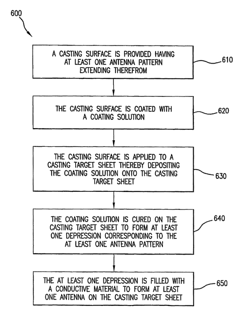
[0043] FIG. 6 illustrates a flowchart 600 of a method for manufacturing RFID
tag antennas, in accordance with an embodiment of the present invention. The
method of flowchart 600 begins at step 610, in which a casting surface is
provided having at least one antenna pattern extending therefrom. For
example, the casting surface can be casting surface 102 (FIG. 1), which has a
raised antenna pattern 104 extending therefrom. The casting surface can be
the surface of a plate (e.g., casting element 103 (FIG. 1)) or a cylinder
(e.g.,
casting element 403 (FIG. 4)).
[0044] In step 620, the casting surface is coated with a coating solution. For
example, the coating solution can be coating solution 120 (FIG. 1).
[0045] In step 630, the casting surface is applied to a target sheet, thereby
depositing the coating solution onto the target sheet. The target sheet call
be,
for example, target sheet 104. The application of the casting surface on the
target sheet is dependent on the particular type of casting element. For
example, when the casting element is a plate, the casting solution is cast on
the
target sheet, in like manner to that described with reference to FIG. 1. In
another example, when the casting element is a cylinder, the casting surface
is
rolled against the target sheet, in like manner to that described with
reference
to FIG. 4.
[0046] In step 640, the coating solution is cured on the target sheet to form
at
least one depression corresponding to the at least one antenna pattern. For
example, the coating solution can be cured by curing agent 106 (FIG. 1) or
curing agent 406 (FIG. 4). That is, curing of the coating solution can occur
after the coating solution is cast (like curing agent 106) or the curing and
casting can occur simultaneously (lilce curing agent 406).
CA 02553213 2006-07-11
WO 2005/067688 PCT/US2005/000879
-11-
[0047] In step 650, the at least one depression is filled with a conductive
material to form at least one antenna on the target sheet. For example,
antenna
material applicator 108 or 408 could fill the at least one depression with the
conductive material.
[0048] FIG. 7 illustrates a flowchart 700 of another method of manufacturing
RFID tag antennas, in accordance with an embodiment of the present
invention. Flowchart 700 begins at step 710, in which a casting element
having a surface that receives a conductive material is provided. For example,
the surface may be casting surface 102 of casting element 103 (FIG. 1) or
casting surface 402 of casting element 403 (FIG. 4); i.e., the casting element
may be a plate, a cylinder, or some other shape. In addition, the casting
surface may have antenna-shaped depressions (e.g. depressions 504 (FIG. 5))
or a raised antenna-shaped pattern (e.g., antenna pattern 204a-d (FIG. 2)). If
the surface has antenna-shaped depressions, the depressions are filled with a
conductive material. If the surface has a raised antenna-shaped pattern, a
sheet
of conductive material (e.g. metal foil) is applied to the surface of the
casting
element.
[0049] In step 720, the casting element is applied to a target sheet to
dispose
the conductive material thereon. For casting element 502 of FIG. 5, the
conductive material that fills antenna-shaped depressions 504 is deposited on
the target sheet (e.g., target sheet 104). For casting element 103 of FIG. 2,
edges of the raised antenna-shaped pattern cut the metal foil, thereby
depositing the metal foil on the target sheet.
[0050] In step 730, the conductive material on the target sheet is cured. For
example, the conductive material can be thermally cured or high-energy
radiation cured, as mentioned above, to form one or more antenna patterns on
the target surface.
IV. Example Advantages
[0051] These embodiments of the present invention fabricate or manufacture
antennas by embossing an extremely accurate and reproducible image of the
antenna. In an example embodiment, an "ultracast" process similar to that
CA 02553213 2006-07-11
WO 2005/067688 PCT/US2005/000879
-12-
developed by SAPPI-NA (South Africa Paper and Pulp Institute-North
America) may be used, whereby an antenna image is embossed using the
"ultracast" process onto a special polymer coating on polyester or paper
target
sheet. Once embossed, the image is cured by an electron beam system. The
casting is done in wide web (60 inch) format and wound in 10,000 feet long
rolls. The cast antenna embossures are extremely accurate and consistent.
Furthermore, the process is non-polluting. Once cast, the rolls are converted
to the width required for input to a tag assembly machine, which may apply
integrated circuit dies and/or otherwise process the antennas. The slit rolls
can
be processed in several iterations to manufacture the RFID antennas.
[0052] By embossing the antenna designs using the above-described casting
process, large volumes of antenna forms can be created in a wide-web format.
The antennas can be made with a greater amount of metal (e.g., silver) than in
a screen-printing process. They can also be made at a lower caliper and
perform better due to the formation of a solid metallic foil.
[0053] Thus, antenna manufacture according to the embodiments described
above may have one or more of the following advantages:
(0054] A. Higher resolution antennas axe formed, for improved performance.
[0055] B. Higher reproducibility is realized, for greater consistency in
antenna
formation.
[0056] C. Higher speed antenna printing is possible, for scalability and
improved
cost.
(0057] D. Higher performance is realized, due to improved metal formation.
[0058] E. Lower cost are realized, due to reduced raw materials, higher
manufacturing speeds, and less waste.
[0059] F. Manufacturing is more environmentally safe due to less waste. For
example, caustic baths resulting from previous antenna manufacturing
techniques are not produced, and therefore disposal thereof is not required.
V. Conclusion
[0060] While various embodiments of the present invention have been
described above, it should be understood that they have been presented by way
CA 02553213 2006-07-11
WO 2005/067688 PCT/US2005/000879
-13-
of example only, and not limitation. It will be apparent to persons skilled in
the relevant art that various changes in form and detail can be made therein
without departing from the spirit and scope of the invention. Thus, the
breadth
and scope of the present invention should not be limited by any of the above-
described exemplary embodiments, but should be defined only in accordance
with the following claims and their equivalents.