Note: Descriptions are shown in the official language in which they were submitted.
CA 02553576 2006-07-13
1
SPECIFICATION
LED AND ATTACHMENT STRUCTURE OF LED
BACKGROUND OF THE INVENTION
Field of the Invention
The present invention relates to an LED and an attachment
structure of an LED which prevent heat accumulation safely and
effectively, which can clamp the voltage of the surface of a
can, and which allow electrically safe mounting.
Description of the Related Art
LEDs have a variety of applications as light emitting
elements. Though there are several types of LEDs, such as a
I5 resin mold type and a can type, an ultraviolet LED, for example,
is greatly deteriorated by ultraviolet light, and emits a large
amount of heat, while output is lowered as the quality of resin
changes in a resin mold type, and therefore, types that are
reliable for a long period of time are limited to the can type.
This can type is provided with an LED pedestal surrounded by
an anode, a cathode and a reflector within a housing, where at
least the connection ends of the anode and the cathode are led
out of the housing, in a manner where a voltage is applied between
the anode and the cathode via these connection ends, for light
emission from the interface between the PN layers of the LED
CA 02553576 2006-07-13
2
element placed within the housing. This light is reflected from
the reflector so as to be guided to a transparent portion made
of glass which is attached to the housing, in the configuration
of the can type LED. The housing is generally made of a metal.
In such a can type, it is difficult to avoid deterioration
in the light emitting property caused by the heat transmission
and heat accumulation accompanying light emission, as well as
negative effects on durability and longevity caused by heat
stress. According to the prior art, however, no examples are
cited where a heat radiation structure is actively adopted.
Fig. 14 illustrates an illumination device 1 for product
inspection which is appropriate for use in the case, for example,
where products are inspected using reflected illumination.
This illumination device 1 is formed of a surface la for mounting
light emitting bodies in a curved concave form, such as the inner
surface of a cylinder or the concave surface of a cone, and of
a great number of LEDs 2, which are denselymounted on this surface
la for mounting light emitting bodies without intervening space .
However, it has conventionally been thought that it is
difficult to provide a heat radiation structure on the rear
surface of surface la for mounting light emitting bodies which
curves in this illumination device 1. Therefore, no specific
heat radiation member is provided behind LEDs 2 but providing
an air layer AS that intervenes between LEDs 2 and a frame member
1b, which merely allows natural heat radiation toward this air
CA 02553576 2006-07-13
3
layer AS (Japanese Unexamined Patent Publication No. 10-21729).
Therefore, a structure that makes active heat radiation
possible has been examined, wherein, as shown in Figs. 11 to
13, a housing 21 placed beneath a transparent portion 21x which
forms an LED2 is formed of a material having a high thermal
conductance, and one of connection ends al and k1 of an anode
A and a cathode K is made to make metallic contact with housing
21 in one of lead positions 21a and 21k (21k in the figure) provided
in housing 21, so that heat can be radiated to the air from housing
21. Though in this example, a reflector R conceptually works
as the above described cathode K which conducts to a body 21b
of the housing, reflector R may be formed in housing 21 by means
of digging in a manner where the structure allows cathode K to
be mounted in a mounting hole provided in body 21b of the housing.
In this case also, reflector R, housing 21 and cathode K are
in a condition where they are mutually conductive . In the figures,
symbols 10a and lOb indicate wiring patterns. The same effects
as in such a structure can be gained in the case where the anode
A side is made to conduct to reflector R and housing 21.
SUMMARY OF THE INVENTION
In the case where an LED having such a heat radiation
structure is adopted, however, housing 21 is charged with either
the polarity of anode A or that of cathode K, and therefore,
short-circuiting or discharge occurs between housing 21,
CA 02553576 2006-07-13
4
connection ends al, k1 and the like of adjacent LEDs 2, causing
a fire in some cases, becoming a large factor for reducing the
reliability, durability and safety of the apparatus in the case
where LEDs 2 are densely placed to form illumination device 1.
Accordingly, a new LED having an internal structure which
can highly efficiently prevent heat accumulation, and which can
effectively avoid the occurrence of short-circuiting and
discharge between LEDs, as well as fire, even in the case where
LEDs are densely placed, and an attachment structure of an LED
are desired.
In order to achieve this object, the present invention
provides the following means.
An LED of the present invention is a can type LED provided
with an anode, a cathode and an LED pedestal within a housing
in a manner where at least the connection ends of the anode and
the cathode are led out to the outside of the housing for a voltage
applied between the anode and the cathode via these connection
ends, characterized in that the insulating condition is
maintained between the connection end of the above anode
and the housing, as well as between the connection end of the
above described cathode and the housing, and in that a lead end
that is thermally connected to the above described LED pedestal
is provided outside of the housing.
Here, the LED pedestal includes a type in a condition where
the LED pedestal is surrounded by the reflector.
CA 02553576 2006-07-13
In such a manner, heat in the LED pedestal, which is the
main heat accumulating portion, can effectively be let out to
the outside of the housing via a connection end. In addition,
an external configuration where heat is further released to an
5 appropriate portion from the connection end can also be applied,
and therefore, it becomes possible to secure a sufficient heat
radiation area by selecting a portion of which the space is not
easily restricted as a heat radiation portion.
In addition, the housing is electrically disconnected from
both the anode and the cathode, and therefore, it becomes possible
to effectively avoid the occurrence of a potential difference
between a housing and a connection end of adj acent LEDs which
becomes the cause of short-circuiting and discharge, even in
the case where LEDs are placed relatively densely.
I5 It is desirable to make an electrical connection between
the housing and the lead end of the LED pedestal of which the
voltage is clamped to the ground or the like, in order to prevent
the potential of the housing from becoming unstable.
It is effective to form at least a portion of the housing,
in addition to the lead end of the LED pedestal, of an insulating
material, in contrast with the formation of the connection ends
of the anode and the cathode of a conductive material, in order
to make it possible for a metal to make contact with the housing
so as to directly draw out heat.
It is preferable for the lead position of the lead end
CA 02553576 2006-07-13
6
to be set directly beneath the LED pedestal, or to be set in
a portion which is approximately in line with the center of the
transparent portion that is attached to the housing, together
with the LED pedestal, in order to effectively draw out heat
from the LED pedestal.
It is effective to align the lead position of the lead
end in line with the lead positions of the respective connection
ends of the anode and the cathode, in order to provide a flexible
connection to an object of which the form is unknown.
It is appropriate to place an LED element on the LED pedestal
in an electrically insulated condition, in order to gain the
effects of the present invention.
It is preferable to connect a diode between the anode and
the cathode in an anti-parallel manner within the housing, in
order to effectively protect the LED from static electricity
and surge voltage. It is especially desirable for this diode
to be a Zener diode.
In this case, it is desirable to use an insulating plate
of which the surface is processed with a metal for a Zener diode
pedestal in the configuration where the Zener diode is installed
within the housing via the 2ener diode pedestal in order to make
the Zener diode function appropriately.
As for a preferable attachment structure of an LED having
an anode, a cathode and an LED pedestal within a housing in the
case where the anode and the cathode are connected to wiring
CA 02553576 2006-07-13
7
patterns provided on a substrate, a structure having a lead end
which is thermally connected to the above described LED pedestal
outside of the above described LED, where a heat radiation pattern
or a cooling pattern is provided independently of the wiring
patterns on the above described substrate and the lead end of
the above described LED is thermally connected to this heat
radiation pattern or cooling pattern can be cited. Here, the
cooling pattern indicates a heat radiation pattern, a portion
of which a cooling source for actively cooling the system is
connected to.
It is desirable for the above described lead end of the
LED that has been mounted on the substrate to be electrically
connected to the heat radiation pattern or the cooling pattern
of the above described substrate, in order to prevent the
potential of the lead end of the LED from becoming unstable.
In this case, it is desirable to form the heat radiation
pattern or the cooling pattern on the rear surface of the substrate
on which the wiring patterns are formed, in order to appropriately
provide both the wiring patterns and the heat radiation pattern
or the cooling pattern for effective heat radiation.
Alternatively, as for another preferable attachment
structure of an LED having an anode, a cathode and an LED pedestal
within a housing in the case where the above described anode
and cathode are connected to wiring patterns provided to the
substrate, a structure having a lead end which is thermally
CA 02553576 2006-07-13
8
connected to the above described LED pedestal outside of the
housing of the above described LED, where a heat radiation member
or a cooling member is directly attached to the rear surface
of the above described substrate and the lead end of the above
described LED is thermally connected directly to this heat
radiation member or the cooling member, or thermally connected
indirectly to this heat radiation member or the cooling member
via a heat radiation pattern or a cooling pattern provided
independently of the above described wiring patterns is cited.
Here, the cooling member indicates a heat radiation member, a
portion of which a cooling source for actively cooling the system
is connected to.
In order to enhance the heat radiation effect, it is
effective to make the width of the heat radiation pattern or
the cooling pattern greater than the width of the wiring patterns
by a large margin. The width of the wiring patterns should
naturally be determined to be a width that allows a required
amount of current to flow, from the point of view of inductance,
heat emission and the like, while the width of the heat radiation
pattern or the cooling pattern is set in consideration of the
waste heat effect, irrespectively of the amount of current
carrying capacity. Accordingly, large margin refers to a case
where the width of the heat radiation pattern or the cooling
pattern is clearly different from the standardwidth of the wiring
patterns which corresponds to the allowed amount of current
CA 02553576 2006-07-13
9
carrying capacity. In the case where the width of the wiring
patterns is set to the above described standardwidth, for example,
large margin refers to the width of the heat radiation pattern
or the cooling pattern being greater than the width of the wiring
patterns. Of course, it is not necessary for the width to be
great throughout the entire portion of the heat radiation pattern
or the cooling pattern, but rather, there may be a portion of
a small width. The same effects can be gained in the case where
the pattern allows heat to be effectively conveyed to a portion
which is wider, outside of the area to which the LED is attached.
Furthermore, large margin can refer to an average width gained
by dividing the integrated pattern area by the integrated pattern
distance being greater than that of the wiring patterns.
Alternatively, in the case where slits divide the cooling pattern
or the heat radiation pattern into a plurality of portions, each
of which has a width smaller than that of the wiring patterns,
that is to say, in the case where, substantially, one heat
radiation pattern or cooling pattern appears to be a pattern
with a small width due to slits, the sum of the widths of the
respective portions which run generally parallel with slits in
between is considered to be the width of the pattern, according
to the present invention, in view of the heat radiation effect.
It is desirable in the above attachment structure for the
housing to be electrically connected to the lead end of the LED
pedestal so as to be voltage clamped, for example, connected
CA 02553576 2006-07-13
to the ground, in order to prevent the potential of the housing
from becoming unstable.
In addition, the above described LED and the attachment
structure of an LED have significant working effects in the case
5 where they are applied to an ultraviolet LED having a large amount
of heat emission. This is because, as described above,
ultravioletLEDsare greatly deteriorated by ultravioletlight,
and emit a large amount of heat, and therefore, types that are
reliable for a long period of time are limited to the can type.
10 A way to prevent heat accumulation in such a can type without
causing short-circuiting or discharge has been widely desired.
As described above, according to the present invention,
even in the case where LEDs are placed relatively densely,
internal heat accumulation can be effectively prevented, while
effectively avoiding short-circuiting, discharge, breaking,
fire and the like, and it becomes possible to increase the
reliability, durability and safety of the apparatus without fail
when this type of LED is utilized.
BRIEF DESCRIPTION OF THE DRA~nIINGS
Fig. I is a perspective view conceptually showing the
appearance of an LED according to one embodiment of the present
invention;
Fig. 2 is a perspective view conceptually showing a heat
radiating structure, together with the internal structure of
CA 02553576 2006-07-13
11
the LED;
Fig. 3 is a cross-sectional view of a portion of the LED;
Fig. 4(a) is a plan view of the LED;
Fig. 4 (b) is a diagram for illustrating a function of the
LED;
Fig. 5 is a front view of the LED;
Fig. 6 is a view showing a modification of the present
invention;
Fig . 7 is a view showing another modification of the present
invention;
Fig. 8 (a) is a cross-sectional view along line VIII-VIII
of Fig. 7;
Fig. 8 (b) is a view showing a modification other than the
above modifications of the present invention;
I5 Fig. 9 is a cross-sectional view conceptually showing a
ring type illumination device to which LEDs are attached;
Fig. 10 is a graph showing the relationship between the
amount of current carrying capacity and the standard width of
wiring patterns;
Fig. 11 is a view conceptually showing the appearance of
an LED conventionally used;
Fig. 12 is a perspective view conceptually showing a
conventional heat radiating structure, together with the
internal structure of the LED conventionally used;
Fig. 13 is a front view of the LED conventionally used;
CA 02553576 2006-07-13
12
and
Fig. 14 is a cross-sectional view schematically showing
a ring type illumination device to which LEDs are attached.
DESCRIPTION OF THE PREFERRED EMBODIMENTS
In the following, one embodiment of the present invention
is described in reference to the drawings.
The attachment structure of an LED according to this
embodiment is applied to the mounting of an LED 3 which has a
structure slightly different from that described above on a
substrate 100 that forms surface la for mounting light emitting
bodies of illumination device 1 for product inspection using
reflected illumination shown in Fig. 12. Fig. 9 shows an
illumination device 1 for product inspection using reflected
illumination, on which LEDs 3 according to this embodiment are
mounted, and which is substantially the same as that shown in
Fig. 12, except for that the portion that corresponds to the
air layer in Fig. 12 is filled in with a heat radiation member
X in Fig. 9. A silicone filling or the like can be cited as
an example of this heat radiation member X. In the case where
frame 1b is made of aluminum, this frame 1b maybe formed so as
to occupy the portion which approximately corresponds to the
air layer, and a heat radiation plate may intervene between frame
1b and LEDs 3.
The attachment structure of this embodiment is
CA 02553576 2006-07-13
13
appropriately used when LEDs 3 are primarily ultraviolet LEDs,
referred to as can type as described in the prior art, having
a so-called three-pin structure where three pins lead out from
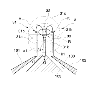
housing 31, as shown in Figs. 1 to 7. That is to say, an LED
3 has an LED pedestal 31p that is surrounded by an anode A, a
cathode K and a reflector R within housing 31, in a manner where
pins (generally referred to as leads) al and k1, which are the
connection ends of anode A and cathode K, lead to the outside
from lead positions which are set in a base 31b in disc form
that forms housing 31, so that a voltage for light emission from
the interface between the PN layers in an LED element 32 placed
within housing 31 can be applied between anode A and cathode
Kvia these pins al and k1. This light is reflected from reflector
R so as to be guided to a transparent portion 31c, which either
transparent or translucent, provided to housing 31 above base
31b, as described above. Reflector R is formed through digging
so as to be provided on base 31b. Transparent portion 31c made
of approximately spherical body of resin or glass, has a lens
function and is placed so as to seal base 31b.
It is preferable to use silicone, a composite resin
(anti-UV resin) or the like as the resin.
In addition, in the present embodiment, a lead end leads
to the outside of housing 31 as the third pin r1 in the condition
where the lead end is thermally connected to the above described
LED pedestal 31p, while maintaining a condition of insulation
CA 02553576 2006-07-13
14
between pin al of the above described anode A and base 31b of
housing 31, as well as between pin k1 of the above described
cathode K and base 31b of housing 31.
Concretely speaking, through holes 31a and 31k, as well
as mounting hole 31r, are provided in lead positions set at the
bottom of housing 31, and pins a1 and k1 of anode A and cathode
K are inserted into corresponding through holes 31a and 31k,
in a condition of isolation, and at the same time, pin r1 which
leads out from LED pedestal 31p is made to make direct contact
with corresponding mounting hole 31r, or is made to make indirect
contact with mounting hole 31r via a heat radiating elastomer
( for example, a heat radiating silicone rubber or a heat radiating
resin) having a high thermal conductance, so that mounting hole
31r is thermally and electrically connected to pedestal 31p.
Base 31b of housing 31 is, of course, made of a material having
high electrical and thermal conductivity.
Pin r1 is located in a portion directly beneath LED pedestal
31p which is positioned at the center of reflector R, and the
lead position of this pin r1 is positioned at the center of base
31b in a disc form. The top of transparent portion 31c having
an approximately spherical surface which covers base 31b of
housing 31 becomes the center 3lcx of the spherical surface,
and the lead position of the above described pin r1 is located
in a portion directly beneath center 3lcx of this transparent
portion 31c. In addition, pins al and k1 of anode A and cathode
CA 02553576 2006-07-13
K are positioned on both sides of pin r1 which is thermally
connected to LED pedestal 31p, and these pins al, k1 and r1 have
a positional relationship where they are aligned approximately
in a straight line.
5 Pin r1, together with housing 31, is formed of a material
having high electrical and thermal conductivity. Spaces
between pins al and k1 of anode A and cathode K, and the sides
of through holes 31a and 31k which are provided in respectively
corresponding lead positions of housing 31 are filled in with
10 an insulating material z, such as glass or a silicone rubber,
in order to maintain a condition of insulation. An insulating
layer 33 having a high thermal conductivity, such as an epoxy
resin, an imide based resin, alumina or aluminum nitride,
intervenes between LED element 32 and LED pedestal 31p. In Fig.
15 5, symbols 34a and 34k indicate conductor wires (bonding wires) .
In addition, as shown in Fig. 4 (a) , a Zener diode 2D makes
a connection between anode A and cathode K in an anti-parallel
manner within housing 31. Fig. 4(b) shows a circuit diagram
thereof, where the LED itself is provided with a defense against
static electricity and surge voltage without losing its
properties . This Zener diode ZD is placed on 2ener diode pedestal
31z within housing 31, and an insulating plate of which the surface
is processed with a metal is used for this Zener diode pedestal
31z.
Meanwhile, patterned substrate 100 of Fig. 5, to which
CA 02553576 2006-07-13
16
LEDs 3 according to the present embodiment are connected, is
utilized as surface for mounting light emitting bodies la of
Fig.9, and is processed with copper or the like using a mask,
so that pairs of wiring patterns 101 and 102 which correspond
to the two polarities are formed. In addition to these wiring
patterns 101 and 102, a heat radiating pattern 103 on which a
masking process of polyimide or the like is carried out is provided
independently of (that is to say, without crossing) the above
described wiring patterns. The width of this heat radiating
pattern 103 has a large margin relative to the width of wiring
patterns 101 and 102. The relationship between the width of
wiring patterns 101 and 102, and the allowable amount of current
carrying capacity is naturally determined in consideration of
inductance and heat emission, while the width of heat radiating
pattern 103 is set in consideration of the waste heat effect,
irrespectively of the amount of current carrying capacity.
Accordingly, large margin indicates a case where the width of
heat radiating pattern 103 is clearly different from the standard
width of wiring patterns 101 and 102 that corresponds to the
amount of current carrying capacity. In the case where the
allowable amount of current carrying capacity is 1 A, for example,
the standard width is 1 mm when the wiring patterns are made
of copper and have a thickness of 30 microns, and in the case
where the amount of current carrying capacity increases or
decreases, the standard width is proportionally increased or
CA 02553576 2006-07-13
l~
decreased. Fig. 10 illustrates alternative relationships
between the allowable amount of current carrying capacity and
the standard width. This figure is a graph showing the relations
between the amount of current carrying capacity and the standard
width for a number of temperatures, with the standard width along
the lateral axis and the amount of current carrying capacity
along the longitudinal axis, in the case where the wiring patterns
are made of a copper foil and have a thickness of 105 Vim. The
width of heat radiating pattern 103 is determined in
consideration of the heat radiating effect, without depending
on the relationships of this graph, and therefore, becomes a
width which is greater than these wiring patterns when a heat
radiating area is secured as effectively as possible on the
substrate surface. Thus, the difference between these widths
becomes a useful margin, in view of easy recognition of heat
radiating pattern 103 relative to wiring patterns 101 and 102,
and prevention of mistakes in the attachment of an LED. Symbol
104 indicates an insulating coating film, such as an epoxy resin
or an imide based resin that covers the surface of the substrate.
In addition, respective pins al and k1 of anode A and cathode
K are connected to the above described wiring patterns 101 and
102, and pin r1, which is thermally connected to LED pedestal
31p, is connected to heat radiating pattern 103.
As described above, an LED 3 of the present embodiment
is provided with pin r1 which is thermally connected to LED
CA 02553576 2006-07-13
18
pedestal 31p outside of housing 31 while keeping a condition
of insulation between pin al of anode A and housing 31, as well
as between pin k1 of cathode K and housing 31.
Accordingly, an LED 3 having this structure can make heat
in LED pedestal 31p, which is a primary heat accumulating portion,
be effectively conveyed to the outside of housing 31 via pin
r1, as shown by the arrows in Fig. 5. In addition, in the case
where pin r1 leads out in such a manner, a configuration for
releasing heat to an appropriate portion, such as heat radiating
pattern 103, can also be gained, as shown in the figure, and
therefore, it becomes possible to secure a sufficient heat
radiating area by selecting a portion which is not subjected
to a spatial restriction as a heat radiating portion.
In addition, housing 31 is electrically insulated from
anode A and cathode K, and therefore, even in the case where
illumination device 1 of Fig. 9 is formed by densely placing
LEDs 3, it becomes possible to effectively avoid the occurrence
of a potential gap, which may cause short-circuiting, and
discharge between housings 31 and 31, as well as between housings
31 and pins al and k1, of adjacent LEDs 3, effectively protecting
LEDs 3, and effectivelyenhancingthe reliability of illumination
device 1.
In particular, housing 31 and pin r1 are electrically
connected to each other, and therefore, housing 31 can be actively
voltage clamped by utilizing pin r1, and the potential of housing
CA 02553576 2006-07-13
19
31 can be maintained without fail at a level which is desirable
for avoiding a discharge and the like, thus gaining the effects
of the present invention. In addition, the lead position of
pin r1 is set in a portion directly beneath LED pedestal 31p,
which is the portion closest to LED pedestal 31p and has a small
thermal resistance, and therefore, the present invention
provides a high thermal conduction, in a manner where heat release
can be expected to be effectively carried out.
In particular, the lead position of pin r1 is set in a
portion which is approximately aligned with center 3lcx of
transparent portion 31c that is attached to housing 31, together
with LED pedestal 31p, and therefore, light emitted from LED
3 can be efficiently guided to transparent portion 31c, avoiding
as much as possible the conversion of the emitted light to heat,
and at the same time, a release of the generated heat can be
expected to be efficiently carried out.
Here, the lead position of pin r1 is aligned in an
approximately straight line with the lead posit ions of respective
pins al and k1 of anode A and cathode K, and therefore, even
in the case where LED 3 is attached to a location that is
three-dimensionally curved, as the surface of a cone shown in
Fig. 9, this LED 3 can be attached in a manner where the direction
of the generatrix of this cone becomes the same as the direction
of the alignment of the pins, without being negatively affected
by the curve, and it becomes possible to effectively avoid poor
CA 02553576 2006-07-13
condition of attachment caused by the three-pin structure.
In addition, LED element 32 is placed on LED pedestal 31p
in a condition of electrical isolation, and therefore, pin r1
can be prevented without fail from being negatively affected
5 by anode A and cathode K via LED pedestal 31p.
Here, in the present embodiment, 2ener diode 2D makes
connection between anode A and cathode K in an anti-parallel
manner within housing 31, providing an effect where LED 3 protects
itself from static electricity and surge voltage. This Zener
10 diode 2D is installed within housing 31 on 2ener diode pedestal
31z where an insulating plate of which the surface is processed
with a metal is used for this Zener diode pedestal 31z, and
therefore, the properties of the diode can be appropriately
prevented from being changed due to the effects of anode A and
15 cathode K, and thus the above described effects can be gained.
Similar effects can, of course, be gained by using a conventional
diode instead of the Zener diode.
Meanwhile, taking into consideration that substrate 100
to which anode A and cathode K are connected is conventionally
20 required for the attachment of such an LED 3, and heat radiating
pattern 103 is provided to this substrate 100 independently of
wiring patterns 101 and 102 so that LED 3 can be connected, in
the present embodiment, and therefore, a heat radiating area
can be effectively formed in a simple pattern formation process,
where substrate 100, which is an existing part, can be effectively
CA 02553576 2006-07-13
21
utilized without introducing a new member for heat radiation.
In addition, a plurality of LEDs 3 are connected to this heat
radiating pattern 3, and thereby, uniform heat diffusion can
be expected from all of LEDs 3. In particular, heat radiating
pattern 103 need not be connected throughout the entirety and
may have a disconnection in the middle, as long as an effective
heat releasing area can be secured, unlike wiring patterns 101
and 102, and therefore, can be designed much more easily, and
can undergo a masking process much more easily, in comparison
with wiring patterns 101 and 102.
Furthermore, the width of heat radiating pattern 103 is
greater than the width of wiring patterns 101 and 102 by a large
margin, and therefore, it becomes possible to secure a sufficient
heat radiating area in heat radiating pattern 103 for further
effective heat release.
Conventionally, it has been believed that it is difficult
to adopt a heat radiating structure in the case where LEDs 3
are densely placed on the surface of a substrate which spreads
in three dimensions, as is seen in this illumination device,
and therefore, the effects that are gained by applying the present
invention areextremelylarge. In addition,theworking effects
of the above described LED 3 and the attachment structure thereof
are extremely significant in the case where they are used for
an ultraviolet LED having a large amount of heat emission or
for an attachment structure of ultraviolet LEDs having a large
CA 02553576 2006-07-13
22
amount of heat emission.
Here, the concrete configurations of the respective
portions are not limited to those in the above described
embodiment. At least a portion of the housing, for example,
may be formed of insulating material, together with pin r1, which
is the lead end of LED pedestal 31p. In this manner, it becomes
possible for the housing to make direct contact with a metal
having high heat conducting properties for heat radiation. In
addition, as shown in Fig. 6, it is also effective to form heat
radiating pattern 103 on rear surface 100b of substrate surface
100a on which wiring patterns 101 and 102 are formed. By doing
so, heat radiating pattern 103 is formed on a different surface
from wiring patterns 101 and 102, and a sufficient heat radiating
area can be secured, making heat radiation effective.
In addition, as shown in Fig. 7, a heat radiating member
40 may be directly attached to the rear surface of substrate
100 as a heat radiating area, and pin r1 may be connected to
this heat radiating member 40 . In the case where it is necessary
to cover rear surface 100b of substrate 100 with an insulating
member, for example, an effective heat radiating structure can
be simply implemented by utilizing this insulating member as
the above described heat radiating member 40. In the drawings,
symbol 103 indicates a heat radiating pattern, and symbols 101
and 102 indicate wiring patterns.
Here, in the example of Fig. 7, heat radiating member 40
CA 02553576 2006-07-13
23
is placed on base 400 made of aluminum. Therefore, in the case
where this base 400 is used as a heat sink by providing a heat
radiating structure 400x, such as fins, to this base 400, it
becomes possible to efficiently release heat that has been
conducted from heat radiating member 40 to base 400.
It is of course effective to form a cooling structure 400y
by providing a water jacket, as shown in the figure, within base
400, in place of or in addition to heat radiating structure 400x.
In this case, heat radiating member 40 is provided with a cooling
source, and therefore, it corresponds to a cooling member,
according to the present invention, rather than to a heat
radiating member. A cooling source may, of course, be connected
to the above described heat radiating pattern 103 so as to function
as the cooling pattern of the present invention.
Alternatively, an effective configuration can be gained
by making an electrical connection of pin r1, which is the lead
end of LED 3 that has been mounted on the substrate, to heat
radiating pattern 103 on the above described substrate, or to
a cooling pattern where a cooling source is added to the heat
radiating pattern so as to achieve a voltage clamp. Also, the
pin r1 as the lead end of the LED 3 may be connected to a heat
radiating member or a cooling member through the heat radiating
pattern or the cooling pattern.
Furthermore, it is possible to provide a structure where
pin r1 penetrates heat radiating member 40 so as to be directly
CA 02553576 2006-07-13
24
connected to base 400, which is a heat sink, in the case where
the voltage clamp is not negatively affected.
Fig. 8 (a) is an enlarged cross-sectional view along line
VIII-VIII of Fig. 7 in the case where a number of LEDs 3 are
placed longitudinally and laterally without intervening space.
As shown in this figure, heat radiating patterns 103, to which
pins r1 of respective LEDs 3 are connected, are connected to
each other, and these heat radiating patterns 103 are formed
avoiding the portions where pins al and k1 of at least anodes
A and cathodes K of respective LEDs 3 penetrate substrate 100.
Accordingly, in the condition where a great number of LEDs 3
are longitudinally and laterally aligned, heat radiating
patterns 103 exhibit a grid or an analogous pattern, as shown
in the drawing, in a manner where the portions where pins al
and k1 of anodes A and cathodes K penetrate substrate 100 form
islands which are isolated from heat radiating patterns 103,
exhibiting a dotted pattern or an analogous pattern when viewed
as a whole . Heat radiating patterns 103 secure the heat radiating
area by utilizing as large an available area of substrate 100
as possible, and the figure clearly shows that the width of the
heat radiating patterns is greater than that of wiring patterns
101 and 102 . Of course, the same holds in the case where a cooling
pattern is formed.
In addition, though in the above described embodiment,
the lead position of a pin r1 is aligned in an approximately
CA 02553576 2006-07-13
straight line with the lead positions of pins al and k1 of anode
A and cathode K, it is also possible to place pins r1, al and
k1 in a manner where they form a triangle as viewed in the plane,
as shown in Fig. 8 (b) , in order to enhance the strength of the
5 attachment, as long as the basic working effects of the present
invention are gained.
In addition to the above, a variety of modifications are
possible in a scope which does not deviate from the gist of the
present invention, such that the present invention is applicable
10 to a variety of LED arrays, including a segment.