Note: Descriptions are shown in the official language in which they were submitted.
CA 02554675 2006-07-26
WO 2005/076692 PCT/IB2004/004430
-1-
10
LIGHT DISPLAY STRUCTURES
BACKGROUND OF THE INVENTION
Field of the invention
The present invention relates generally to light displays.
Description of the Related Art
A variety of light display structures have been provided in response
to the advantageous features of light-emitting diodes (e.g., low voltage,
low heating, low maintenance, color diversity and long life). These
structures, however, have generally been complex and expensive to
produce.
BRIEF SUMMARY OF THE INVENTION
Simple, inexpensive light display structures of the present
invention are formed with various structures that facilitate the
energizing of a plurality of light-emitting elements that are coupled
between first and second conductors.
The novel features of the invention are set forth with particularity
in the appended claims. The invention will be best understood from the
following description when read in conjunction with the accompanying
drawings.
CA 02554675 2006-07-26
WO 2005/076692 PCT/IB2004/004430
-2-
BRIEF DESCRIPTION OF THE DRAWINGS
FIGS. 1A and 1B are top and side views of a light display structure
embodiment of the present invention and FIG. 1C is an enlarged view of
another embodiment for structure within the curved line 1C of FIG. 1B;
FIG. 2 is an enlarged isometric view of the light display structure of
FIGS. 1A and 1B that illustrates additional light display structures;
FIGS. 3A-3D are views along the plane 3-3 of FIG. 1B that
illustrate additional light display structures;
FIG. 4 is an isometric view of the light display structure of FIG. 3C
which emphasizes its flexible, elongate form;
FIGS. 5A and 5B are views of additional light display structures
that can be carried on the structure of FIG. 4;
FIGS. 6A-6C are enlarged plan views of another light display
structure embodiment of the present invention
FIGS. 7A and 7B are enlarged views along the plane 7-7 of FIG. 6B
that illustrate additional light display structures;
FIG. 8 is an enlarged view similar to FIG. 6B that illustrates
additional light display structures;
FIG. 9 is an enlarged view along the plane 9-9 of FIG. 8 that
illustrates additional light display structures;
FIG. 10A is a top view of another light display structure
embodiment of the present invention;
FIG. 10B is a view along the plane 10B-10B of FIG. 10A;
FIG. lOC is a top view of another light display structure
embodiment of the present invention; and
FIG. 10D is a view along the plane lOD-10D of FIG. lOC.
DETAILED DESCRIPTION OF THE INVENTION
FIGS. 1-10D illustrate light display structure embodiments that
can be economically fabricated and quickly assembled to energize a
plurality of light-emitting elements in a variety of light displays. In
particular, FIGS. 1A and 1B illustrate a display structure embodiment
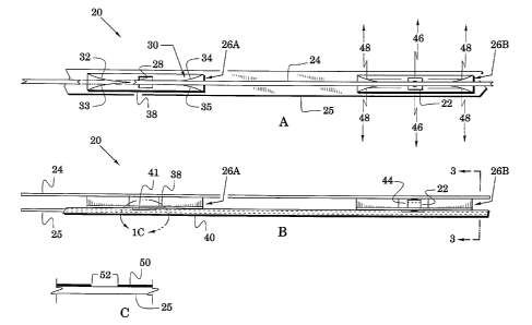
20 for energizing at least one light-emitting element 22. The structure
CA 02554675 2006-07-26
WO 2005/076692 PCT/IB2004/004430
-3-
includes first and second elongate conductors 24 and 25 and at least one
spacer 26 that is positioned between the first and second conductors.
As indicated by a spacer 26A, the spacers each define an aperture
28 to receive the light-emitting element as it contacts the first and
second conductors 24 and 25. The spacer 26A illustrates the aperture 28
while the spacer 26B illustrates reception of the light-emitting element
22 into the aperture. Each spacer 26 also defines at least one light
redirector 30 that is positioned to redirect light away from its respective
light-emitting element 22.
In particular, the light redirector may be configured in any of
various forms (e.g., a reflective wall or a refractive wall) that will direct
at least a portion of the light away from the spacer. For simplicity, the
light redirector will subsequently be referred to as a wall which may be
flat in one embodiment. In another embodiment, it preferably has a
concave shape as shown in FIG. 1A. In another embodiment, the wall
may have a substantially parabolic shape to enhance redirection of the
light.
In the structure embodiment of FIGS. lA and 1B, each spacer 26
defines first and second walls 32 and 33 that diverge with increasing
distance from one side of their aperture 28 and third and fourth walls 34
and 35 that diverge with increasing distance from another side of their
aperture 28. In one embodiment, the spacer may include a base 38 that
defines the aperture 28 and the walls extend upward from the base.
As shown in FIG. 1B, the display structure may include a polymer
(e.g., a thermoplastic or a thermosetting polymer) insulator 40 that
encloses the second conductor 25. In this case, the insulator preferably
defines an opening 41 positioned to facilitate contact between the light
emitting element and the second conductor 25. The spacers 22 are
positioned to space the first and second conductors apart locally while
the insulator 40 insures they do not contact elsewhere.
Although the light display structures of the invention may carry
various light-emitting elements, the structure 20 of FIGS. 1A and 1B is
especially suited to carry a light-emitting diode (LED) which is received
in the aperture 28 with its cathode in contact with the second conductor
25 and its anode in contact with the first conductor 24.
CA 02554675 2006-07-26
WO 2005/076692 PCT/IB2004/004430
-4-
In operation of the light display structure 20, a voltage is applied
between the first and second conductors 24 and 25 which energizes the
LED and causes light to be emitted from its light-emitting junction 44.
As shown in FIG. 1A, the light radiates from the junction so that some
light rays 46 issue directly away from the spacer 26B and other light rays
48 are redirected by the walls 32-34 to also radiate away from the spacer
26B.
As shown in FIG. 1C, another display structure may apply (e.g., by
printing, transfer printing, silkscreening) an insulator 50 on the second
conductor 25. The insulator is arranged (e.g., by masking or by ablating)
to define a gap or aperture 52 into which the LED is received, i.e., the
insulator 50 is configured to permit coupling of the LED to the second
conductor.
The enlarged isometric view 60 of FIG. 2 supplements FIGS. 1A and
1B. It shows a strip 62 that facilitates fabrication of the spacers (26 in
FIGS. lA and 1B). The strip can be easily molded from a polymer and
has a base 38 that defines apertures 28 and walls 30 that extend upward
from the base. For example, the walls may include the first and second
walls 32 and 33 that diverge with increasing distance from one side of
their aperture 28 and the third and fourth walls 34 and 35 that diverge
with increasing distance from another side of their aperture 28. Although
not required, the diverging walls preferably abut at their ends that are
proximate to their respective aperture. The walls terminate in a back
wall 63 and a top wall 64.
A light-emitting element 22 in the form of an LED is shown in the
process of being received into an aperture 28. Joining elements 65 and 66
are preferably formed of conductive materials (e.g., conductive epoxy,
solder, reflow solder) and are provided to join the diode's anode to the
first conductor 24 and the diode's cathode to the second conductor 25.
This operation insures electrical continuity between the first and second
conductors and their respective contacts of the LED. When a voltage is
imposed between the conductors, the LED is energized and light is
radiated from the diode's junction 44 and at least a portion of that light
is redirected latterly away from the conductors 24 and 25 by the walls 30.
The strip 62 may be formed with a notch 68 that facilitates
CA 02554675 2006-07-26
WO 2005/076692 PCT/IB2004/004430
separation of one spacer from an adjoining spacer. As shown in FIG. 2,
various other strip embodiments may be formed. For example, the spacer
structure 70 defines two wall structures that face oppositely to be
operative with apertures 28A and 28B. In an assembly process, spacers
can be easily broken from the strip 62 (with aid, for example, from the
notch 68) and spaced along the first and second conductors as shown in
FIGS. 1A and 1B.
The first and second conductors 24 and 25 and their spacers 26 may
be enclosed with various substantially-transparent structures to form
elongate radiating elements. For example, FIG. 3A (a view along the
plane 3-3 of FIG. 1B) shows them enclosed in a thermoplastic shrink
tube 80 and FIG. 3B shows them enclosed by a thermoplastic molded
cover 82 (the spacer's back wall 63 is indicated in each of these figures).
In FIG. 3C, the cover 82 has been modified to a cover 84 that defines a
mounting surface 85 that can abut, for example, a floor or wall.
In FIG. 3D, the cover 82 of FIG. 3B has been modified to a cover 86
that defines a pair of protrusions 87 in addition to defining the mounting
surface 85 of FIG. 3C (the protrusions appear as outward-extending ribs
when envisioned in the elongate structure 90 of FIG. 4 which is described
below). Because of the flexible nature of these protrusions or ribs, they
flex and absorb the pressure of an impinging object (e.g., a pedestrian's
shoe) to thereby prevent damage to light-emitting elements within (as
shown in FIG. 2).
In FIG. 3E, the cover 82 of FIG. 3B has been modified to a cover 88
that defines a mounting flange 89 which can facilitate attachment (e.g.,
with adhesive, with mechanical elements such as rivets or by sewing) to
various objects (e.g., footwear, clothing apparel and architectural
mountings).
Structures such as those of FIGS. 3A-3E can be used to form
elongate light display structures such as the structure 90 of FIG. 4 which
can be bent into various forms and which radiates light laterally when a
voltage is placed across the first and second conductors 24 and 25.
Transparent or translucent decorative figures 92 can be molded in
various forms that slide onto (or snap over) the structure 90 as shown in
FIG. 5A. Alternatively, a decorative figure 94 can include a hinged
CA 02554675 2006-07-26
WO 2005/076692 PCT/IB2004/004430
-6-
member 95 (a non-engaged position is shown in broken lines) which
facilitates its installation over the structure 90 as shown in FIG. 5B.
FIGS. 6A-6C illustrate another display structure embodiment 100
for carrying at least one light-emitting element 22. As shown particularly
in FIG. 6A, a spacer 102 is shaped to define an array of apertures 22 and
also to define an array of cup-shaped walls 104 that each surround a
respective one of the apertures. FIG. 6B shows an array of light-emitting
elements 22 that are each received in a respective one of the apertures.
FIG. 6B also shows a plurality of first conductors 24 that each contact a
first side of a selected group of the light-emitting elements 22. These
conductors are also shown in FIG. 7A which is an enlarged view along the
plane 7-7 of FIG. 6B.
In particular, FIG. 7A shows the spacer 102 positioned to space the
first and second conductors 24 and 25 with a light-emitting element
received in an aperture to contact the first and second conductors. The
second conductor 25 may comprise a plurality of elongate conductors
(similar to the first conductors 24 in FIG. 6B) or may comprise a
conductive sheet that contacts all of the light-emitting elements of FIG.
6B.
In one light display embodiment, the light-emitting elements are
LEDs which radiate light from their light-emitting junctions 44. When a
voltage is placed across the first and second conductors, the LEDs are
energized and light rays 106 are radiated from the junction 44 and
redirected laterally from the plane of the spacer 102 by the cup-shaped
wall 104 as shown in FIG. 7A.
The first conductors 24 of FIG. 6B are shown to have a linear form
but this is one of many possible embodiments. FIG. 6C, for example,
shows a first elongate conductor 24A which is configured to contact
various selected light-emitting elements that do not lie along a linear
path. These elements can be selected so that the radiated light forms
various figures (e.g., a letter, a number or a word) from the array of light-
emitting elements.
The cup-shaped wall 104 of FIG. 7A is shown to have a concave
shape which may be substantially parabolic to enhance the redirected
radiation. FIG. 7B is similar to FIG. 7A with like elements indicated by
CA 02554675 2006-07-26
WO 2005/076692 PCT/IB2004/004430
-7-
like reference numbers. Similar to the spacer 102 of FIG. 7A, a spacer
110 is positioned to space the first and second conductors and it defines
an array of apertures to each receive a respective one of the light-emitting
elements 22 as it contacts respective ones of the first and second
conductors.
In contrast to the spacer 102, however, the spacer 110 defines a
cup-shaped wall 112 that has a flat shape rather than the concave shape
of the wall 104 of FIG. 7A. Also the spacer 110 spaces the first and
second conductors apart without completely filling the space between
these conductors. Instead, the spacer 110 comprises a sheet that is
formed to define the cup-shaped wall 112 and to contact the second
conductor 25 locally and contact the first conductor 24 in other regions.
FIG. 8 illustrates another light-emitting structure 120 which is
similar to the structure 100 of FIG. 6B with~like elements indicated by
like reference numbers. The structure 120, however, includes a
substantially-transparent sheet 122 formed of a suitable polymer
(e.g., mylar). The first conductors 24 can be bonded to the sheet 122 and
the sheet is then placed to bring these conductors into contact with their
respective light-emitting elements 22.
As shown in FIG. 9 (a view along the plane 9-9 of FIG. 8), the sheet
122 and its first conductors 24 may be locally shaped to form dimples
124 that enhance contact between the conductors and their respective
light-emitting elements 22. In another light-emitting structure
embodiment, the sheet 124 may carry photoluminescent films 126 (e.g.,
phosphor films, conjugated polymer, organic phosphor). In operation of
this embodiment, light rays 128 from the light-emitting element 22 are
redirected by the cup-shaped wall (104 in FIG. 8) to strike the phosphor
films. In response to this excitation, the luminescent films emit light
rays 130. Different luminescent films may be used to selectively display
different colors.
Semiconductor LEDs have been configured to emit light with a
variety of wavelengths and, generally, the forward voltage drop of these
LEDs increases as the wavelength decreases. For example, red, yellow
and green LEDs typically exhibit forward voltage drops in the respective
ranges of 1.8-2.0 volts, 2.0-2.2 volts and 2.2-2.5 volts. In addition, each
CA 02554675 2006-07-26
WO 2005/076692 PCT/IB2004/004430
_ g _
LED typically has a specified forward current that is recommended to
enhance LED performance parameters (e.g., intensity, dissipation and
lifetime).
Accordingly, it may be desirable to insert a resistive member
between the LEDs of the light display structures and their associated
first and second conductors. This is exemplified in FIG. 2 where a
resistive member 136 (e.g., a resistive film such as a thin film resistor, a
thick film resistor, conductive paste, conductive epoxy) is inserted
between the anode of the LED 22 and the first conductor 24 (the insertion
is indicated by insertion arrow 138 - e.g., the member can be carried over
the anode). Alternatively, the resistive member may be inserted between
the cathode of the LED 22 and the second conductor 25.
The resistivity and cross section of the resistive member 136 are
configured to realize a predetermined resistance which will provide the
specified forward current when a selected supply voltage is applied via
the first and second conductors 24 and 25. An exemplary green LED, for
example, is specified to have a forward voltage drop of 2.8 volts and a
forward current of 20 milliamps. For this particular LED, the resistivity
and cross section of the resistive member 136 would preferably be
configured to provide a resistance that increases through the range of 10
to 100 ohms when the selected supply voltage increases through the
range of 3.0 to 4.8 volts.
In general, the resistivity and cross section of the resistive member
136 are chosen to realize the specified forward current in response to a
provided supply voltage. To enhance conductivity between elements,
conductive films may be carried on the anode and cathode surfaces and
also inserted between the resistive member and its associated one of the
first and second conductors.
FIGS. 10A-10D illustrate other light display embodiments of the
present invention. In particular, FIG. 10 A shows a light display
embodiment 140 in which the first and second conductors 24 and 25 are
arranged (e.g., side by side) to facilitate the insertion of wire bonds 142
that couple a selected one of the anode and cathode surfaces (wherein the
anode surface has been selected in FIG. l0A) of LEDs 22 to the first
conductor 24.
CA 02554675 2006-07-26
WO 2005/076692 PCT/IB2004/004430
-9-
As shown .in FIG. lOB, a resistive member 136 (introduced in FIG.
2) is preferably inserted between the LED 22 and the wire bond 142. In
addition, the LED's anode and cathode (and the resistive member 136)
may be joined to the wire bond 136 and the second conductor 25 with
conductive elements 65 and 66 (also introduced in FIG. 2).
FIG. lOC illustrates a light display embodiment 160 that is similar
to the embodiment 140 of FIG. 10A with like elements indicated by like
reference numbers. In this embodiment, however, the first conductor 24 is
modified to a conductor 164 which defines a plurality of tabs 166. Each of
the LEDs 22 is then coupled between the second conductor 25 and a
respective one of the tabs 166. FIG. lOD is similar to FIG. lOB except
that the conductor 164 and its tab 166 is substituted for the first
conductor 24 and the wire bond 142.
The light display embodiments of FIGS. 10A-lOD may also be
enclosed with various substantially-transparent structures to form
elongate radiating elements. In FIGS. 3A-3D, for example, they can be
substituted for the light display embodiments of FIGS. lA-1C and 2
(which are represented in FIGS. 3A-3D by first and second conductors 24
and 25 and a spacer's back wall 63).
The light display structure embodiments shown in FIGS. 1-lOD are
simple and comprise few parts so that they can be economically
fabricated from various polymers and quickly assembled. They lend
themselves for realization in a variety of forms. For example, they can be
realized in elongate display structures wherein light is directed laterally
from the elongate shape or sheet-like display structures wherein light is
directed laterally from the sheet. The descriptions of these embodiments
include walls which are light redirectors that may be configured in
various forms (e.g., reflective or refractive walls).
The spacers (e.g., 26, 102) shown in various ones of the figures, the
insulator 40 of FIG. 1B, the tube 80 of FIG. 3A, the cover 82 of FIG. 3B
and the transparent sheet 122 of FIGS. 8 and 9 can be fabricated from
various insulators such as polymers (e.g., polyimide and mylar). The first
and second conductors (24 and 25 in FIG. 2) may be formed from various
conductive metal foils (e.g., copper and silver). The spacers may also be
fabricated in colors that enhance the light redirected from their
CA 02554675 2006-07-26
WO 2005/076692 PCT/IB2004/004430
- 10 -
respective LEDs.
In an exemplary display embodiment, the photoluminescent films
126 of FIG. 9 may include conjugate polymers and organic phosphors that
are excited, for example, by blue LEDs to thereby cause the redirected
light rays 130 to be substantially white.
The embodiments of the invention described herein are exemplary
and numerous modifications, variations and rearrangements can be
readily envisioned to achieve substantially equivalent results, all of
which are intended to be embraced within the spirit and scope of the
invention as defined in the appended claims.