Note: Descriptions are shown in the official language in which they were submitted.
CA 02554913 2006-07-31
F-P06087SI(CA)
SPECIFICATION
MANUFACTURING METHOD FOR SEMICONDUCTOR
PHOTOELECTROCHEMICAL CELL AND SEMICONDUCTOR
PHOTOELECTROCHEMICAL CELL
BACKGROUND OF THE INVENTION
1. FIELD OF THE INVENTION
The present invention relates to a manufacturing method for
a semiconductor photoelectrochemical cell and a semiconductor
photoelectrochemical cell, and in particular, to a manufacturing
method for a semiconductor photoelectrochemical cell having
photocatalyst effects and a semiconductor photoelectrochemical
cell which is manufactured in accordance with this method.
2. DESCRIPTION OF THE RELATED ART
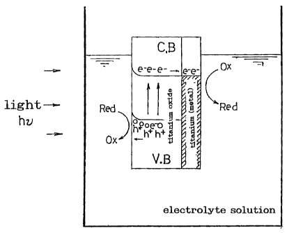
When light hits single crystal or microscopic particles of an N
type oxide semiconductor such as titanium oxide in an electrolyte
solution as shown in Fig. 5, electrons in a valence band (V.B) are
excited and move to a conduction band (C.B). An oxidation reaction
(Red -+ Ox) occurs in the vicinity of holes (h+) from which electrons
have been removed in the valence band while a reduction reaction
(Ox -> Red) occurs in the vicinity of the conduction band where the
excited electrons (e-) exist.
In the contact interface between the electrolyte solution and
the semiconductor, however, the band curves due to a Schottky
barrier, so that no reduction reaction occurs unless electrons move
1
CA 02554913 2006-07-31
F-P06087SI(CA)
over this barrier. Therefore, only a slight amount of electrons
contribute to the reduction reaction, and accordingly, the oxidation
reaction occurs only slightly.
It was clarified in 1972, however, that electrolysis of water
due to light can be induced by using platinum for the counter
electrode in a semiconductor photoelectrochemical cell (NATURE
Vol. 238, No. 5358, pp. 37-38 (1972)). In addition to this, it is
known that similar effects can be gained by connecting platinum
electrodes to titanium oxide single crystal or making microscopic
particles of titanium oxide carry microscopic particles of platinum
(CHEMICAL PHYSICS LETTERS Vol. 88, No. 1, pp. 50-54 (1982)). In
this case, platinum is made to be carried using a method where a
substance gained by reducing titanium oxide immersed in a platinic
acid with formaldehyde is heated at a high temperature.
According to the above described prior art, however, in any
event, expensive platinum is used for electrodes, and the
manufacturing method for electrodes is also complicated, so that it
is hard to say that the art is practical. After the above described
findings, one of the present inventors developed a method according
to which titanium is burned at 700 C to 800 C and thereby N type
semiconductor having anatase type crystal can be generated, and
titanium is burned at 1200 C to 1500 C and thereby N type
semiconductor having rutile type crystal can be fabricated (Japanese
Unexamined Patent Publication No. H6 (1994)-90824), buy in this
case, efficient photocatalyst effects cannot be provided by mixing an
2
CA 02554913 2006-07-31
F-P06087SI(CA)
appropriate amount of titanium metal in a titanium oxide layer that
is formed on the surface after burning.
Furthermore, though an invention relating to a method for
manufacturing a photocatalyst material by carrying out anodic
oxidation on titanium metal and burning this in an atmosphere of
500 C has been proposed (Japanese Unexamined Patent Publication
No. 2000-271493), the preprocessing is complicated, and thus, this
cannot be said to be a simple or practical method.
SUMMARY OF THE INVENTION
Therefore, an object of the present invention is to provide, in
view of the problems with the above described prior art, a
manufacturing method for a semiconductor photoelectrochemical
cell which can be manufactured in accordance with a simple method
without using an expensive precious metal and has excellent
photocatalyst effects, as well as a semiconductor
photoelectrochemical cell that is manufactured in accordance with
this method.
The above described object is achieved by the inventions
according to the claims. That is to say, the manufacturing method
for a semiconductor photoelectrochemical cell according to the
present invention is characterized by providing such a configuration
that a base made of titanium or a titanium alloy is burned in an
atmosphere of 700 C to 1000 C with a rate of temperature increase
of no less than 5 C/second, so that a titanium oxide layer is formed
3
CA 02554913 2006-07-31
F-P06087SI(CA)
on the surface and titanium metal is mixed in the above described
titanium oxide layer.
In this configuration, a semiconductor photoelectrochemical
cell having excellent photocatalyst effects in which no expensive
material such as a precious metal is used for an electrode, and a
photocatalyst reaction which is more reactive than those gained in
the prior art occurs when irradiated with light, so that a large
electromotive current flows, can be gained.
As shown in Fig. 1, titanium metal is adjacent to titanium
oxide in the structure of a cell according to the present invention,
and therefore, in the interface, no Schottky barrier as that in the
contact interface between the electrolyte solution and the
semiconductor is formed, and therefore, electrons that receive light
energy can be easily excited to a conduction band, an efficient
reduction reaction occurs in the titanium metal portion, and an
efficient oxidation reaction occurs in the semiconductor portion.
This is different from the prior art, where, as shown in Fig. 5, a
Schottky barrier is formed in the entirety of the contact interface
between the entire surface of the semiconductor and the electrolyte
solution. Accordingly, in the case of the cell according to the
present invention, the efficiency of the photocatalyst reaction
becomes significantly higher in comparison with the prior art, so
that a greater electromotive current is generated for a same
intensity of irradiated light, or an efficient photocatalyst reaction
occurs for a smaller amount of irradiated light. In a case where the
4
CA 02554913 2006-07-31
F-P06087SI(CA)
temperature for burning is lower than 700 C, the efficiency of
generation of titanium oxide as an N type oxide semiconductor is
poor, and sufficient photocatalyst effects cannot be gained, and in a
case where the temperature for burning exceeds 1000 C,
photocatalyst effects cannot be gained either. The temperature for
burning preferably exceeds 810 C and is no higher than 1000 C. In
addition, in a case where the rate of temperature increase at the
time of burning is lower than 5 C/second, an appropriate amount of
titanium metal cannot be mixed into the titanium oxide layer that is
generated on the surface of the base after burning, which is not
preferable.
As a result, a manufacturing method for a semiconductor
photoelectrochemical cell which is manufactured in accordance with
a simple method without using an expensive precious metal and has
excellent photocatalyst effects, can be provided.
In addition, the manufacturing method for a semiconductor
photoelectrochemical cell according to the present invention may be
characterized by providing such a configuration that a base made of
titanium or a titanium alloy is burned in an atmosphere of 900 C to
1000 C to form a titanium oxide layer on the surface, and after that,
quenched in cold water to mix titanium metal in the above described
titanium oxide layer.
Also in this configuration, a semiconductor
photoelectrochemical cell having excellent photocatalyst effects in
2 5 which no expensive material such as a precious metal is used for an
5
CA 02554913 2006-07-31
F-P06087SI(CA)
electrode and a photocatalyst reaction having higher activity than
that gained in the prior art occurs when irradiated with light, and a
large electromotive current flows, can be gained. In this case, the
temperature for burning is high, and therefore, generated oxide
coating layer having high insulating properties can be easily
removed through quenching, so that titanium metal can be mixed
into the titanium oxide layer in the lower structure. It is preferable
for such cold water to be no warmer than 10 C.
It is preferable to additionally carry out mechanical
processing in order to partially remove the above described
generated titanium oxide layer, so that the surface area of titanium
metal in the above described titanium oxide layer becomes 10 % to
30%.
In this configuration, a titanium metal layer can be surely
exposed from the titanium oxide layer. Thereby, for the mechanical
processing, such a method for partially removing the titanium oxide
layer by creating slits using a polisher or the like or filing or cutting
the surface of the titanium oxide layer using a jig such as a file or a
cutting tool, may be adopted. In addition, in the case where the
surface area of titanium metal that has been exposed from the above
described titanium oxide layer is 10 % to 30 % of the surface area of
the titanium oxide layer, stable and efficient photocatalyst effects
can be gained. In a case where the surface area of titanium metal is
less than 10 %, it is difficult to gain efficient photocatalyst effects,
while in a case where the surface area of titanium metal exceeds
6
CA 02554913 2010-09-02
30 %, photocatalyst effects gained from the titanium oxide layer are
reduced.
The configuration of the semiconductor
photoelectrochemical cell according to the present invention is
characterized in that the semiconductor photoelectrochemical cell
is manufactured in accordance with a manufacturing method for a
semiconductor photoelectrochemical cell according to the present
invention, as described herein.
In this configuration, a semiconductor photoelectrochemical
cell which is manufactured in a simple method without using an
expensive precious metal and has excellent photocatalyst effects can
be provided.
BRIEF DESCRIPTION OF THE DRAWINGS
Fig. 1 is a diagram showing a photocatalyst reaction in a
semiconductor photoelectrochemical cell according to the present
invention;
Fig. 2 is a flow chart schematically showing a manufacturing
process for the semiconductor photoelectrochemical cell of Fig. 1;
Fig. 3 is a is a diagram showing a method for measuring an
electromotive current in the examples and comparative examples;
Fig. 4 is a graph showing a change in pH indicating
decomposition of lactic acid by the semiconductor
photoelectrochemical cell of Fig. 1; and
Fig. 5 is a diagram showing a photocatalyst reaction in the
7
CA 02554913 2006-07-31
F-P06087SI(CA)
semiconductor photoelectrochemical cell according to the prior art.
DETAILED DESCRIPTION OF THE PREFERRED EMBODIMENTS
The embodiments of the present invention are described in
detail with reference to the drawings. Fig. 2 is a flow chart
schematically showing a manufacturing process for a semiconductor
photoelectrochemical cell according to the present embodiment.
Titanium or a titanium alloy can be used for a base used for a
semiconductor photoelectrochemical cell according to the present
embodiment, and an appropriate form thereof can be selected in
accordance with the application with no particular limitations, like
plate form, rod form or bulb form. An example using pure titanium
(purity: no lower than 99.0 %) in rod form is cited in the description.
First, it is preferable to wash with acid the base made of
titanium in rod form in advance (#1). The washing with acid can be
carried out in accordance with a conventional, known method, for
example, by immersing the base in 5 wt% to 10 wt% of a hydrofluoric
acid solution for a predetermined period of time.
After stains and the like on the surface of the base is washed
with acid and removed, the base is sufficiently washed with water
(#2) and polished so that the surface become smoother, if necessary
(#3).
Then, the base is burned in the atmosphere (#4), so that a
coating film of titanium oxide is formed on the surface of the base.
The temperature for heating is 700 C to 1000 C, and more preferably,
8
CA 02554913 2006-07-31
F-P06087SI(CA)
exceeds 810 C and is no higher than 1000 C. such temperature is
kept for one minute to two hours, more preferably 4 minutes to 30
minutes.
After keeping the base at a predetermined temperature for a
predetermined period of time, the base is quenched in cold water of
no warmer than 10 C (#5), so that cracking occurs in the titanium
oxide coating film that is formed on the surface of the base, and thus,
the oxide coating film is partially removed. Though the coating film
naturally falls off in many cases, it may be mechanically removed if
necessary. As a result, the surface of the base has a structure where
titanium oxide and titanium metal coexist. In this case, the
thickness of the titanium oxide coating film is approximately 0.1 pm
to 30 pm, and more preferably, approximately 0.5 pm to 10 pm.
Next, slits are created on the base where the titanium oxide
coating film has been formed using a polisher or the like (#6). This
is for surely and stably exposing titanium metal from the surface of
the base, and an appropriate form and number of slits can be selected,
and it is preferable to create silts in such a manner that the surface
area of the exposed titanium metal becomes approximately 10 % to
30 % of the titanium oxide layer. In the case where the exposed
area of titanium metal is greater than this, the photocatalyst effects
of the titanium oxide become smaller, which is not preferable. The
step of creating slits, however, is not always necessary, and may be
omitted when the exposed area of titanium metal is made great by
quenching the base after the base is burned at a high temperature.
9
CA 02554913 2006-07-31
F-P06087SI(CA)
Examples
<Burning Test>
(Example 1)
A pure titanium (99.5 wt%) rod having a diameter of
approximately 3 mm and a length of approximately 80 mm was used
as a base. This base was washed with an acid, that is, a hydrofluoric
acid solution, in advance and dried, and after that, heated and
burned in an atmosphere of 1000 C for 4 minutes to 30 minutes at a
rate of temperature increase of ? C/second in an electrical furnace,
and then quenched in cold water of approximately 10 C. The ratio
of exposure of titanium metal on the surface of the titanium oxide
layer was found from the surface area of the base after X ray images
of Ti and 0 were taken using an EPMA (JXA-8800RM, made by JEOL
Ltd.). In the case of Example 1, the outermost surface layer having
high insulating properties was removed through quenching, and
approximately 20 % of titanium metal was mixed into the titanium
oxide layer in the lower structure portion.
(Example 2)
The same processing as that in Example 1 was carried out,
except for that the rate of temperature increase was set at
5 C/second and the sintering temperature was set at 810 C. In
Example 2, though the outermost surface layer was not removed
through quenching, titanium oxide on the generated surface did not
have high insulating properties, and it was found that approximately
CA 02554913 2006-07-31
F-P06087SI(CA)
20 % of titanium metal was mixed into the titanium oxide layer when
the structure was observed.
(Example 3)
The same processing as that in Example 2 was carried out,
except for that the temperature for burning was set at ?00 C. The
outermost surface layer was not removed in this example, even
through quenching, as in Example 2.
(Comparative Example 1)
The same processing as that in Example 2 was carried out,
except for that the temperature for burning was set at 1200 C. In
this case, though the uttermost surface layer having high insulating
properties was removed through quenching as in Example 1, almost
no titanium metal was mixed into the titanium oxide layer in the
lower structure portion.
(Comparative Example 2)
The same processing as that in Example 2 was carried out,
except for that the temperature for burning was set at 500 C. In
this case, the outermost surface layer was not removed even through
quenching, as in Examples 2 and 3, and generation of the titanium
oxide layer was insufficient.
The electromotive current was measured for each of Examples
1 to 3 and Comparative Examples 1 and 2 in accordance with the
following method. That is to say, a sample of each of the above
described examples and comparative examples was put into a
container containing a 0.1 % saline solution as an electrolyte
11
CA 02554913 2006-07-31
F-P06087SI(CA)
solution, and an electrode in rod form where platinum was plated on
a titanium metal was used as a counter electrode 2. As shown in Fig.
3 (showing only an example where Example Sample 1 is used), these
two electrodes 1 and 2 were electrically connected to each other via
a current meter 3, and this was used with the light source (light
energy: hv) of a fluorescent lamp (6 W), so that the flowing current
was measured. The results of measurement are shown in Table 1.
It can be seen from Table 1 that an electromotive current of
which the level is higher than that of the comparison examples was
generated in Examples 1 to 3, where the base was heated at a
temperature of 700 C to 1000 C for 4 minutes to 30 minutes. It is
more preferable for the base to be burned at 810 C to 1000 C.
<Effects of Quenching>
Next, Table 2 shows the results of measurement of an
electromotive current in the case where the sample of Embodiment
1 was quenched in cold water of no warmer than 10 C, as well as in
the case where the sample was naturally cooled in the atmosphere
after being taken out of the furnace. In the case where the sample
was not quenched after being burned at 1000 C, a thick titanium
oxide coating film covered the surface, preventing an appropriate
amount of titanium oxide from being mixed into a titanium metal,
and a great electromotive current could not be generated.
In addition, in the case where the temperature for burning
was 700 C to 810 C, though no titanium oxide coating film was
2 5 removed through quenching, an appropriate amount of titanium
12
CA 02554913 2006-07-31
F-P06087SI(CA)
oxide and titanium metal could be mixed into the surface, and a large
amount of photoelectromotive current could be generated, due to
the high rate of temperature increase (no less than 5 C/second), in
addition to the above.
<Effects of Rate of Temperature Increase>
Table 3 shows the effects of the rate of temperature increase.
In the case where the rate of temperature increase was lower than
5 C/second when the base was burned in an atmosphere of 700 C to
1000 C, an appropriate amount of titanium metal could not be mixed
into the titanium oxide layer that was generated on the surface of
the base after burning, and a large amount of photoelectromotive
current could not be generated. In particular, in the case of lower
than 900 C (700 C to 810 C), a large amount of photoelectromotive
current could not be generated when the rate of temperature
increase was low.
<Lactic Acid Decomposing Test>
Next, a lactic acid decomposing test was carried out using the
sample of the above described Example 2 (of which the time for
burning was 4 minutes). Lactic acid was diluted to 0.01 % with 0.3
M of a potassium sulfate solution, and furthermore, sodium
hydroxide was added, and thereby, the pH was adjusted to 5.7. The
sample of Example 2 was put into 2 mL of this lactic acid solution,
and this was irradiated with light from a 20 W chemical lamp from a
distance of 2.5 cm (A). The pH was measured using a commercially
available pH meter (M-8, made by Horiba, Ltd.). For the purpose of
13
CA 02554913 2006-07-31
F-P06087SI(CA)
comparison, the change in the pH in the case where the sample of
Example 2 was put into the above described lactic acid solution but
this was not irradiated with light (B) is shown together with the
change in pH of only the above described lactic acid solution (C).
Here, in order to accelerate mixing of the solution, bubbling with
oxygen was used. Fig. 4 shows the change in the pH during the
course of irradiation in this case.
It can be seen from Fig. 4 that decomposition of lactic acid in
the lactic acid solution into which the sample of the above described
Example 2 was put progressed when irradiated with light, and in this
case, it can also be seen that the photocatalyst reaction surely
progressed. In this case, lactic acid decomposed through a
photocatalyst reaction so as to change to pyruvic acid, as shown in
the following formulas. Furthermore, generated hydrogen ions were
reduced by electrons (e-) in a conduction band of titanium metal, and
the pH increased.
CH3CHOH000H+2p+--*CH3000OOH+2H+
CH3000OOH+2H++2e--+CH3000OOH+H2
[Other Embodiments]
(1) Though pure titanium is cited as an example of a base in the
description of the above described embodiments, various types of
titanium alloys, such as titanium-aluminum-vanadium alloys,
titanium-molybdenum-zirconium alloys and titanium-aluminum-tin
alloys can be used as the base in the present invention.
(2) A semiconductor photoelectrochemical cell according to the
14
CA 02554913 2006-07-31
F-P06087SI(CA)
present invention can be widely used in the food industry, chemical
industry, medical industry, environmental equipment industry and
the like, because of its photocatalyst effects.
CA 02554913 2006-07-31
F-P06087SI(CA)
[Table 1]
Time for
Temperature Photoelectromotive
burning
for burning ( C) current (pA)
(minutes)
Example 1 1000 4 24.0
1000 30 9.7
Example 2 810 4 15.8
810 30 9.2
Example 3 700 4 7.2
700 30 8.0
Comparative 1200 4 5.1
Example 1 1200 30 6.9
Comparative 500 4 2.8
Example 2 500 30 3.3
16
CA 02554913 2006-07-31
F-P06087SI(CA)
[Table 2]
Photoelectromotive
Rate of current (pA)
Temperature Time for
temperature When not
for burning burning
increase When quenched
( C) (minutes)
( C/second) quenched (naturally
cooled)
Example 1000 4 7 24.0 1.0
1 1000 30 7 9.7 1.1
Example 810 4 5 15.8 2.3
2 810 30 5 9.2 1.7
Example 700 4 5 7.2 2.0
3 700 30 5 8.0 2.9
17
CA 02554913 2006-07-31
F-P06087SI(CA)
[Table 3]
Rate of
Temperature Time for Photoelectromotive
temperature
for burning burning current (pA) (when
increase
( C) (minutes) quenched)
( C/second)
Example 1000 4 7 24.0
1 1000 30 7 9.7
1000 30 0.5 8.6
Example 810 4 5 15.8
2 810 30 5 9.2
810 30 0.5 4.6
Example 700 4 5 7.2
3 700 30 5 8.0
700 30 0.5 3.6
18