Note: Descriptions are shown in the official language in which they were submitted.
CA 02554942 2006-07-31
WO 2005/083793 PCT/US2004/031984
NITRIDE HETEROJUNCTION TRANSISTORS HAVING
CHARGE-TRANSFER INDUCED ENERGY BARRIERS AND
METHODS OF FABRICATING THE SAME
BACKGROUND OF THE INVENTION
1. Field of the Invention
The present invention relates to high frequency transistors and in particular
relates to
microwave field effect transistors (FETs) that incorporate nitride-based
active layers.
2. Description of the Related Art
The present invention relates to transistors formed of nitride semiconductor
materials
that can make them suitable for high power, high temperature, and/or high
frequency
applications. Materials such as silicon (Si) and gallium arsenide (GaAs) have
found wide
application in semiconductor devices for lower power and (in the case of Si)
lower frequency
applications. These more common semiconductor materials may not be well suited
for higher
power and/or high frequency applications, however, because of their relatively
small
bandgaps (e.g., 1.12 eV for Si and 1.42 for GaAs at room temperature) and/or
relatively small
breakdown voltages.
GaAs based HEMTs have become the standard for signal amplification in civil
and
military radar, handset cellular, and satellite communications. GaAs has a
higher electron
mobility (approximately 6000 cm2/V-s) and a lower source resistance than Si,
which may
allow GaAs based devices to function at higher frequencies. However, GaAs has
a relatively
small bandgap (1.42 eV at room temperature) and relatively small breakdown
voltage, which
may prevent GaAs based HEMTs from providing high power at high frequencies.
In light of the difficulties presented by Si and GaAs, interest in high power,
high
temperature and/or high frequency applications and devices has turned to wide
bandgap
semiconductor materials such as silicon carbide (2.996 eV for alpha SiC at
room temperature)
and the Group III nitrides (e.g., 3.36 eV for GaN at room temperature). These
materials
typically have higher electric field breakdown strengths and higher electron
saturation
velocities as compared to gallium arsenide and silicon.
A device of particular interest for high power and/or high frequency
applications is
the high electron mobility transistor (HEMT), which is also known as a
modulation doped
CA 02554942 2006-07-31
WO 2005/083793 PCT/US2004/031984
field effect transistor (MODFET) or a Heterostructure Field Effect Transistor
(HFET). These
devices may offer operational advantages under a number of circumstances. They
are
typically characterized by the presence of a two-dimensional electron gas
(2DEG) formed at
the heterojunction of two semiconductor materials with different bandgap
energies, where the
smaller bandgap material has a higher electron affinity compared to the larger
bandgap
material. The 2DEG, which forms due to the presence of an accumulation layer
in the smaller
bandgap material, can contain a very high sheet electron concentration in
excess of, for
example, 1013 carriers/cm2 even though the material is nominally undoped.
Additionally,
electrons that originate in the wider-bandgap semiconductor transfer to the
2DEG, allowing a
high electron mobility due to reduced ionized impurity scattering.
This combination of high carrier concentration and high carrier mobility can
give the
HEMT a very large transconductance and may provide a performance advantage
over metal-
semiconductor field effect transistors (MESFETs) for high-frequency
applications, although
MESFETs continue to be suitable for certain applications based on factors such
as cost and
reliability.
High electron mobility transistors fabricated in the gallium nitride (GaN)
material
system have the potential to generate large amounts of RF power because of the
combination
of material characteristics that includes the aforementioned high breakdown
fields, their wide
bandgaps, large conduction band offset, and/or high saturated electron drift
velocity. In
addition, polarization of GaN-based materials contributes to the accumulation
of carriers in
the 2DEG region.
GaN-based HEMTs have already been demonstrated. U.S. Patent No. 6,316,793, to
Sheppard et al., which is commonly assigned and is incorporated herein by
reference,
describes a HEMT device having a semi-insulating silicon carbide substrate, an
aluminum
nitride buffer layer on the substrate, an insulating gallium nitride layer on
the buffer layer, an
aluminum gallium nitride barrier layer on the gallium nitride layer, and a
passivation layer on
the aluminum gallium nitride active structure.
Improvements in the manufacturing of GaN semiconductor materials have focused
interest on the development of GaN HEMTs for high frequency, high temperature
and high
power applications. GaN-based materials have large bandgaps, and high peak and
saturation
electron velocity values [B. Belmont, K. Kim and M. Shur, J.Appl.Phys. 74,
1818 (1993)].
GaN HEMTs can also have 2DEG sheet densities in excess of 10131cm2 and
relatively high
electron mobility (up to 2000 cm2/V-s) [R. Gaslca, J.W. Yang, A. Osinsky, Q.
Chen, M.A.
CA 02554942 2006-07-31
WO 2005/083793 PCT/US2004/031984
Khan, A.O. Orlov, G.L. Snider and M.S. Shur, Appl.Phys.Lett., 72, 707 (1998)].
These
characteristics may allow GaN HEMTs to provide high power at higher
frequencies.
A conventional GaN HEMT structure 110 is illustrated in Figure 14. A channel
layer 114 is formed on buffer layer 113 on a substrate 112. A barrier layer
116 is formed on
the channel layer 114. A source electrode 118 and a drain electrode 120 form
ohmic
contacts through the surface of the barrier layer 116 to the electron layer
that is present at the
top of the channel layer 114. A gate electrode 122 forms a non-ohmic contact
to the surface
of the barrier layer 116.
Typically, the channel layer 114 includes GaN while barrier layer 116 includes
AIGaN. Because of the presence of aluminum in the crystal lattice, AIGaN has a
wider
bandgap than GaN. Thus, the interface between a GaN chamiel layer 114 and an
AIGaN
barrier layer 116 forms a heterostructure or heterojunction where energy bands
are deformed
due to, for example, Fermi level alignment and polarization in the material.
Figure 15 is an exemplary band diagram showing the energy levels in the device
along a portion of section I-I' of Figure 14. As illustrated in Figure 14,
because the barrier
layer 116 has a lower electron affinity (~ than the channel layer 114, when
the Fermi levels
in the materials align due to charge transfer, the energy bands of the channel
layer 114 are
shifted upwards, while those of the barrier layer are shifted downwards. As
shown in Figure
15, using properly designed materials, the conduction band E~ dips below the
Fermi level (Ef)
in the area of the channel layer 114 that is immediately adjacent to barrier
layer 116, forming
a narrow accumulation region. Consequently, a two dimensional electron gas
(2DEG) sheet
charge region 115 is induced in the accumulation region at the heterojunction
between the
channel layer 114 and the barrier layer 116. The barrier layer 116 is made
sufficiently thin so
as to be depleted of mobile carriers by the junction formed with the gate 122
and the resulting
shape of the conduction band.
In addition, in a nitride-based device, the conduction and valence bands in
the barrier
layer 116 are further distorted due to polarization effects. This very
important property of the
heterostructures in the III-Nitride system may be essential for the high
performance of the
GaN HEMT. In addition to the accumulation of electrons due to the bandgap
differential and
band offset between the barrier and channel layers, the total number of free
electrons is
enhanced greatly by pseudomorphic strain in the barrier layer relative to the
channel. Due to
localized piezoelectric effects, the strain causes an enhanced electric field
and a higher
electron concentration than would, typically, be possible were the strain not
present.
CA 02554942 2006-07-31
WO 2005/083793 PCT/US2004/031984
Electrons in the 2DEG sheet charge region 115 demonstrate high carriex
mobility.
Moreover, because the sheet charge region is extremely thin, the carriers are
subject to
reduced impurity scattering that may improve the device's noise
characteristics.
The source to drain conductivity of this device structure is modulated by
applying a
voltage to the gate electrode 122. When a reverse voltage is applied, the
conduction band
beneath the gate is elevated, with the result that the conduction band E~ in
the vicinity of the
sheet charge region 115 becomes elevated above the Fermi level, and a portion
of the sheet
charge region 115 is depleted of carriers, thereby preventing or reducing the
flow of current
from source 118 to drain 120.
By forming the barrier layer 116 from A1N, certain advantages can be achieved.
The
2.4% lattice mismatch between A1N (AlyGal_yN for y=1) and GaN results in an
increased and
even maximum possible piezoelectric charge at the interface between the two
layers. Using
an A1N barrier layer also reduces the piezoelectric scattering between the
layers that can limit
the 2DEG mobility.
However, the high lattice mismatch between A1N and GaN dictates that the
thickness
of the A1N layer should be less than 50 ~. If the layer is thicker, the device
can experience
problems with its ohmic contacts, the material quality in the layer begins to
degrade, the
device's reliability decreases, and the material is more difficult to grow.
However, a HEMT
with a SOA or less A1N layer may be susceptible to high gate leakage.
Although GaN-based HEMTs have demonstrated exceptional power densities, a
number of technical challenges still remain to be overcome before the devices
can achieve
commercial success. For example, one problem that may limit the performance
and lifetime
of certain GaN-based HEMTs is free carrier trapping, which may occur when
carriers migrate
away from the 2DEG region and become trapped in a surface dielectric region or
in a buffer
region beneath the channel. Such trapping may result in degradation in
performance and/or
reliability of a device.
Some attempts have been made to improve confinement of carriers within a HEMT
channel by providing a second heterojunction below the channel - a so-called
Double
Heterostructure HEMT or DH-HEMT. However, in general, the amount of
confinement due
to the heterobarrier (which is a function of the difference in electron
affinity between a wide-
bandgap layer and the narrower-bandgap channel) may not be sufficiently large
to result in
effective confinement. Moreover, in a highly polarized material such as c-
plane GaN, the
polarization charges present in the material may reduce the confinement effect
of the
heterobarrier. Thus, in nitride-based transistor devices, the mere presence of
a heterojunction
CA 02554942 2006-07-31
WO 2005/083793 PCT/US2004/031984
alone below the channel may not~be sufficient to effectively prevent carriers
from migrating
away from the 2DEG region into the buffer region where they can become
trapped.
Moreover, the structure of a DH-HEMT provides no additional barrier against
surface
trapping effects.
Another problem associated with the transit of carriers away from the channel
region
is linearity. When carriers are not confined to the channel, the ability to
control their action
via the applied gate voltage may be reduced, resulting in undesirable
nonlinear
transconductance characteristics.
The problems associated with free carrier trapping may also affect the
performance of
other types of nitride field effect transistors, such as GaN-based MESFETs.
SUMMARY OF THE INVENTION
Embodiments of the present invention provide nitride-based field effect
transistors
having a substrate, a channel layer that includes InAIGaN formed on the
substrate;
source and drain ohmic contacts in electrical communication with the channel
layer;
and a gate contact formed on the channel layer. At least one energy barrier is
formed
between the channel layer and the substrate or between the channel layer and a
surface of the
device opposite the substrate. The energy barrier may include an electron
source layer in
proximity with a hole source layer. The energy barrier has an associated
electric field
directed away from the channel layer. The energy barrier may arise due to
charge transfer
between the electron source layer and the hole source layer and may have a
peak electric field
in excess of about 2x10⁵ V/cm.
Particular embodiments of the invention provide a HEMT capable of high-
frequency
operation that includes a substrate; a channel layer that includes InAIGaN
formed on the
substrate, a barrier layer that includes InAIGaN formed on the channel layer,
the barrier layer
having a bandgap greater than a bandgap of the channel layer. The barrier
layer and the
channel layer cooperatively induce a two-dimensional electron gas at an
interface between
the channel layer and the barrier layer. At least one energy barrier is formed
adjacent the
barrier layer and/or the channel layer, the energy barrier includes an
electron source layer in
proximity with a hole source layer.
In certain embodiments, the electron source layer includes a layer doped with
n-type
dopants. In other embodiments, the electron source layer includes a
heterointerface between
a first InAIGaN layer and a second InAIGaN layer.
CA 02554942 2006-07-31
WO 2005/083793 PCT/US2004/031984
In certain embodiments the electron source layer includes a heterointerface
between
the channel layer and the barrier layer.
The hole source layer may include a layer doped with p-type dopants. In
certain
embodiments, the hole source layer includes a layer co-doped with deep-level
transition
elements and shallow acceptor dopants, or doped with deep level acceptor
dopants.
Alternatively, the hole source layer may include a heterointerface between a
first InAIGaN
layer and a second InAIGaN layer.
The electron source layer and the hole source layer may or may not be fully
depleted
under equilibrium conditions.
An energy barrier according to embodiments of the present invention may
provide a
built-in potential barrier in excess of about O.SV. In particular embodiments,
the energy
barrier may provide a built-in potential barrier in excess of about 1 V. In
further
embodiments, the energy barrier may provide a built-in potential barrier in
excess of about
2V.
Embodiments of the present invention also include forming a channel region and
forming an energy barrier that opposes the movement of carriers away from the
channel
region. Some embodiments of the invention include forming a channel region and
forming
an energy barrier that opposes the movement of carriers away from the channel
region on
each side of the channel region.
In some embodiments, forming an energy barrier includes forming an electron
source
layer, a hole source layer, and a high field region between the electron
source layer and the
hole source layer. In some embodiments, the channel layer may be formed on the
electron
source layer. In other embodiments, the electron source layer may be formed
after formation
of the channel layer.
In particular embodiments, a hole source layer is formed, a high field region
is formed
on the hole source layer, and an electron source layer is formed on the high
field region. A
channel layer is formed on the electron source layer. For HEMT structures, a
barrier layer
may be formed on the channel layer in order to facilitate generation of a 2DEG
region
between the channel layer and the barrier layer.
In other embodiments, a channel layer is formed, an electron source layer is
formed
on the channel layer, a high field region is formed on the electron source
layer and a hole
source layer is formed on the high field region.
In still further embodiments of the present invention, the built-in potential
is
generated by a quantum well adjacent the channel layer. The quantum well may
be provided
CA 02554942 2006-07-31
WO 2005/083793 PCT/US2004/031984
by a first nitride layer adjacent the channel layer and a second Group III-
nitride based layer
adjacent the first nitride layer and opposite the channel layer. The first
nitride layer has a
band gap that is narrower than a band gap of the channel layer and a lattice
constant that is
larger than a lattice constant of the channel layer, and the second Group III-
nitride based
layer has a band gap and a lattice constant that are substantially the same as
the band gap and
lattice constant of the channel layer.
In certain embodiments of the present invention, the first nitride layer is
InN and the
channel layer and second Group III-nitride based layer are GaN. The first
nitride layer may
have a thickness of about one or two monolayers. The channel layer may have a
thickness of
from about 30 ~ to about 300 ~.
DESCRIPTION OF THE DRAWINGS
,.
Figure 1 is a schematic drawing showing a transistor structure according to
embodiments of the present invention.
Figure 1A is a schematic drawing showing a transistor structure according to
further
embodiments of the present invention.
Figure 2 is an illustrative graph showing (a) the charge density, (b) electric
field and
(c) electric potential within a region of the structure of Figure 1.
Figure 3 is an illustrative graph -of the band diagram of a region within the
embodiments illustrated in Figure 1.
Figure 4 is a schematic drawing showing a transistor structure according to
further
embodiments of the present invention.
Figure 5 is an illustrative graph of the band diagram of a region within the
embodiments illustrated in Figure 4.
Figure 6 is a schematic drawing showing a transistor structure according to
further
embodiments of the present invention.
Figure 7 is an illustrative graph of the band diagram of a region within the
embodiments illustrated in Figure 6.
Figure 8 is a schematic drawing showing a transistor structure according to
further
embodiments of the present invention.
Figure 9 is an illustrative graph of the band diagram of a region within the
embodiments illustrated in Figure 8.
Figure 10 is a schematic drawing showing a transistor structure according to
further
embodiments of the present invention.
CA 02554942 2006-07-31
WO 2005/083793 PCT/US2004/031984
Figure 11 is an illustrative graph of the band diagram of a region within the
embodiments illustrated in Figure 10.
Figure 12 is a schematic drawing showing a transistor structure according to
further
embodiments of the present invention.
Figure 13 is an illustrative graph of the band diagram of a region within the
embodiments illustrated in Figure 12.
Figure 14 is a schematic diagram of a prior art HEMT structure.
Figure 15 is an illustrative graph of the band diagram of a region within the
structure
illustrated in Figure 14.
Figures 16-18 are flowcharts illustrating operations according to further
embodiments
of the invention.
DETAILED DESCRIPTION
The present invention will now be described more fully with reference to the
accompanying drawings in which some embodiments of the invention are shown.
This
invention may, however, be embodied in many different forms and should not be
construed
as limited to the embodiments set forth herein. Rather, these embodiments are
provided so
that this disclosure will be thorough and complete, and will fully convey the
scope of the
invention to those skilled in the art. Like numbers refer to like elements
throughout.
Furthermore, the various layers and regions illustrated in the figures are
illustrated
schematically. Accordingly, the present invention is not limited to the
relative size and
spacing illustrated in the accompanying figures. As will also be appreciated
by those of skill
in the art, references herein to a layer formed "on" a substrate or other
layer may refer to the
layer formed directly on the substrate or other layer or on an intervening
layer or layers
formed on the substrate or other layer. As used herein the term "and/or"
includes any and all
combinations of one or more of the associated listed items.
It will be understood that although the terms first, second, etc. may be used
herein to
describe various regions, layers, and/or sections, these regions, layers,
and/or sections should
not be limited by these terms. These terms are only used to distinguish one
region, layer, or
section from another region, layer, or section. Thus, a first region, layer,
or section discussed
below could be termed a second region, layer, or section, and similarly, a
second without
departing from the teachings of the present invention.
As discussed above, confinement of carriers in the channel is an important
concern in
the design of a nitride-based field effect transistor. Embodiments of the
present invention
CA 02554942 2006-07-31
WO 2005/083793 PCT/US2004/031984
may provide enhanced confinement of carriers through the inclusion of a high-
field region on
one or both sides of a channel. The electric field in the high field region
may be generated
by the transfer of charge between an electron source region and a hole source
region. The
electric field in the high field region is directed away from the channel.
Thus, the electric
field opposes the movement of negatively charged electrons away from the
channel. (In
general, the direction of an electric field is defined by the direction of
electric force acting on
a positively charged particle.)
As used herein, the term "Group III nitride" refers to those semiconducting
compounds formed between nitrogen and the elements in Group III of the
periodic table,
usually aluminum (Al), gallium (Ga), and/or indium (In). The term also refers
to ternary and
quaternary compounds such as AIGaN and AIInGaN. As is well understood by those
in this
art, the Group III elements can combine with nitrogen to form binary (e.g.,
GaN), ternary
(e.g., AIGaN, AIInN), and quaternary (e.g., AIInGaN) compounds. These
compounds all have
empirical formulas in which one mole of nitrogen is combined with a total of
one mole of the
Group III elements. Accordingly, formulas such as AIXGaI_XN where 0 S x _< 1
are often used
to describe them. For brevity, when the term AIInGaN is used herein without
specification of
relative percentages for the Group III elements (Al, In and Ga), it will be
understood to refer
to a compound of the general formula InXAIyGaZN where x+y+z=1, 0 _< x _< 1, 0
5 y <_ 1, and 0
5 z <_ 1. Thus, as used herein, the term InAIGaN may refer to GaN, InN, A1N,
AIGaN,
AIInN, InGaN and/or AIInGaN unless otherwise specified or limited.
Accordingly, the terms
"InAIGaN", "Group III-nitride material" and "nitride-based material" are used
interchangeably throughout this specification.
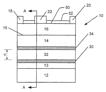
Embodiments of the present invention are schematically illustrated as a high
electron
mobility transistor (HEMT) 10 in the cross-sectional view of Figure 1. The
transistor 10
includes a substrate 12 that may be, for example, semi-insulating silicon
carbide (SiC) of the
4H polytype. Other silicon carbide candidate polytypes including the 2H, 3C,
6H, and 15R
polytypes may be utilized. The term "semi-insulating" is used descriptively in
a relative
sense rather than in an absolute sense. In particular embodiments of the
present invention,
the silicon carbide bulk crystal may have a resistivity equal to or higher
than about 1x10⁵ 52-
cm at room temperature.
A buffer layer 13 on the substrate 12 provides an' appropriate crystalline
transition
between the substrate 12 and the remainder of the device. Buffer layer 13 may
include one or
more layers of InAIGaN. In particular embodiments, buffer layer 13 may include
A1N or
CA 02554942 2006-07-31
WO 2005/083793 PCT/US2004/031984
AIGaN. Silicon carbide has a much closer crystal lattice match to Group III
nitrides than
does sapphire (A1203), which is a very common substrate material for Group III
nitride
devices. The closer lattice match may result in Group III nitride films of
higher quality than
those generally available on sapphire. Silicon carbide also has a very high
thermal
5 conductivity so that the total output power of Group III nitride devices on
silicon carbide is,
typically, not as limited by thermal dissipation of the substrate as in the
case of the same
devices formed on sapphire. Also, the availability of semi-insulating silicon
carbide
substrates may provide for device isolation and reduced parasitic capacitance.
Although silicon carbide is the preferred substrate material, embodiments of
the
10 present invention may utilize any suitable substrate, such as sapphire,
aluminum nitride,
aluminum gallium nitride, gallium nitride, silicon, GaAs, LGO, ZnO, LAO, InP
and the like.
In some embodiments, an appropriate buffer layer also rnay be formed.
Suitable SiC substrates are manufactured by, for example, Cree, Inc., of
Durham,
N.C., the assignee of the present invention, and the methods for producing are
described, for
example, U. S. Patent Nos. Re. 34,861; 4,946,547; 5,200,022; and 6,218,680,
the contents of
which are incorporated herein by reference in their entirety. Similarly,
techniques for
epitaxial growth of Group III nitrides have been described in, for example, U.
S. Patent Nos.
5,210,051; 5,393,993; 5,523,589; and 5,292,501, the contents of which are also
incorporated
herein by reference' in their entirety.
Particular structures for GaN-based HEMTs are described, for example, in
commonly
assigned U.S. Patent 6,316,793, and U.S. application serial no. 09/904,333
filed July 12, 2001
for "ALUMINUM GALLIUM NITRIDE/GALLIUM NITRIDE HIGH ELECTRON
MOBILITY TRANSISTORS HAVING A GATE CONTACT ON A GALLIUM NITRIDE
BASED CAP SEGMENT AND METHODS OF FABRICATING SAME," U.S. provisional
application serial no. 60/290,195 filed May 11, 2001 for "GROUP III NITRIDE
BASED
HIGH ELECTRON MOBILITY TRANSISTOR (HEMT) WITH BARRIER/SPACER
LAYER," United States Patent Application Serial No. 10/102,272, to Smorchkova
et al.,
entitled "GROUP-III NITRIDE BASED HIGH ELECTRON MOBILITY TRANSISTOR
(HEMT) WITH BARRIER/SPACER LAYER" and United States Patent Application Serial
No. 10/199,786, to Saxler, entitled "STRAIN BALANCED NITRIDE HETEROJUNCTION
TRANSISTORS AND METHODS OF FABRICATING STRAIN BALANCED NITRIDE
HETEROJUNCTION TRANSISTORS" the disclosures of which are hereby incorporated
herein by reference in their entirety. Embodiments of the present invention
may be
CA 02554942 2006-07-31
WO 2005/083793 PCT/US2004/031984
11
incorporated into such structures and, therefore, should not be construed as
limited to the
particular structures described in detail herein.
Returning again to Figure 1, a transistor 10 includes a channel layer 14. In
some
embodiments of the present invention, the channel layer 14 includes InAIGaN.
In particular
embodiments, the channel layer 14 includes AlxGa1_XN (0 _< x <_ 1). In some
embodiments of
the present invention, the channel layer 14 includes GaN. The channel layer 14
may be
undoped and may be grown to a thickness of between about 50 and about 500 ~.
Thus, the
channel layer 14 may be thinner than channel layers in conventional GaN HEMT
devices,
which are typically greater than 500 A in thickness. In some of the
embodiments described
above, it may be desirable for the semiconductor crystal structure to be
oriented in a Ga-polar
(or Group III polar) orientation to enhance the effect of the piezoelectric
quality of the
material. However, many of the embodiments, including the embodiment of Figure
1, may
be formed using N-polar or non-polar material without departing from the scope
of the
invention.
1 S A barrier layer 16 is provided on the channel layer 14. The barrier layer
16 may be a
Group III-nitride having a bandgap larger than that of the channel layer 14.
Accordingly, the
barrier layer 16 may be AIGaN, AIInGaN, AIInN and/or A1N. The barrier layer 16
may be at
least about 10 nm thick, but is not so thick as to cause cracking or defect
formation therein.
Moreover, the barrier layer 16 should be thin enough that it is completely
depleted under
equilibrium conditions.
Preferably, the barrier layer 16 is undoped or doped with activated donor
atoms at a
concentration of less than about 1 O19 Cm 3. In some embodiments, the barrier
layer 16 may be
delta-doped at a concentration of up to about 1 O13 Cm 2 at a distance of
about 100 A from the
interface between barrier layer 16 and channel layer 14. In some embodiments
of the
invention, the barrier layer 16 includes AIXGaI_XN where 0 < x < 1. In certain
embodiments
of the present invention, the barrier layer 16 includes AIGaN with an aluminum
concentration
of between about 5% and about 100%. In specific embodiments of the present
invention, the
aluminum concentration is greater than about 10%. The barrier layer 16 has a
bandgap
greater than that of the channel layer 14.
The barrier layer may also be provided with multiple layers as described in
United
States Patent Application Serial No. 10/102,272, to Smorchkova et al.,
entitled "GROUP-III
NITRIDE BASED HIGH ELECTRON MOBILITY TRANSISTOR (HEMT) WITH
BARRIER/SPACER LAYER" and U.S. Patent No. 6,316,793 entitled "Nitride Based
Transistors on Semi-Insulating Silicon Carbide Substrates with Passivation
Layer" issued
CA 02554942 2006-07-31
WO 2005/083793 PCT/US2004/031984
12
November 13, 2001, the disclosures of which are incorporated herein by
reference as if set
forth fully herein. Thus, embodiments of the present invention should not be
construed as
limiting the barrier layer to a single layer but may include, for example,
barrier layers having
combinations of InAIGaN layers having various material compositions. For
example, a
GaN/A1N structure may be utilized to reduce or prevent alloy scattering.
An optional InAIGaN contact layer or cap layer (not shown) may be provided on
the
barrier layer 16 to facilitate the formation of contacts of the transistor 10.
An example of
such a cap layer is disclosed in U.S. application serial no. 09/904,333 filed
July 12, 2001 for
"ALUMINUM GALLIUM NITRIDEIGALLIUM NITRIDE HIGH ELECTRON
MOBILITY TRANSISTORS HAVING A GATE CONTACT ON A GALLIUM NITRIDE
BASED CAP SEGMENT AND METHODS OF FABRICATING SAME," which is
referenced above. In addition, there may be a compositionally graded
transition layer (not
shown) between the barrier layer 16 and the contact or cap layer. The source
contact 18, the
drain contact 20 and the gate contact 22 may be fabricated as described in
U.S. Patent No.
6,316,793.
As discussed above, a 2DEG sheet charge region 15 is induced at the interface
between channel layer 14 and barrier layer 16. In order to reduce the movement
of carriers
away from the channel layer 14, a region 32 having a high electric field is
provided between
the channel layer 14 and the buffer layer 13. In some embodiments, the high
field is
generated by charge transfer between an electron source layer 34 and a hole
source layer 30
which are spaced apart by a distance "d" which defines the thickness of the
high field region
32.
In some embodiments, including the embodiment illustrated in Figure 1, the
electron
source layer 34 may include a thin layer of a Group III-nitride material such
as AlXGa1_XN (0
< x < 1) that is highly doped with donor (n-type) dopants, while the hole
source layer 30 may
include a thin layer of a Group III-nitride material such as AIXGaI_XN (0 < x
< 1) that is
highly doped with acceptor (p-type) dopants. The electron source layer 34 and
the hole
source layer 30 are spaced apart by a distance "d" that defines a high field
region 32
therebetween. When the electron source layer 34 and the hole-source layer 30
are formed,
chaxge transfer between the layers occurs to cause the Fermi levels of the
layers to align (i. e.
to ensure that under equilibrium conditions, the average electron energy is
the same
throughout the structure). This charge transfer causes a depletion region to
form between the
electron source region and the hole source region. The chaxge transfer may
fully deplete the
electron source region and/or the hole source region. The depletion region is
characterized
CA 02554942 2006-07-31
WO 2005/083793 PCT/US2004/031984
13
by a high electric field directed away from the channel layer 14. The
magnitude of the
induced electric field is proportional to the doping levels in the electron
source layer and the
hole source layer. A built-in potential is developed between the electron
source layer and the
hole source layer that is proportional to the thickness of the~high field
region (i. e. the distance
between the electron source region and the hole source region. Accordingly, by
selecting
appropriate values for the thickness, doping level and spacing of the electron
source layer 34
and the hole source layer 30, a potential barrier up to the bandgap (less the
donor and
acceptor ionization energies) may be formed. However, it may be preferable to
provide a
potential barrier somewhat less than the theoretical maximum, for example less
than about
3eV for GaN (which has a nominal bandgap of about 3.SeV).
Moreover, the buffer 13 may be doped with deep acceptors as described in S.
Heikman et al., Growth of Fe-Doped Semi-insulating GaN by Metalorganic
Chemical Vapor
Deposition, Appl. Phys. Let. 81, pp. 439-441 (2002). Specific examples of co-
doped layers
are provided in U.S. Patent Application Serial No. entitled "Co-Doping for
Fermi
Level Control in Semi-Insulating Group III Nitrides" (Atty. Docket 5308-371),
filed January
7, 2004 and assigned to the assignee of the present invention, the disclosure
of which is
incorporated herein by reference. The buffer could be doped with Fe or another
deep
acceptor.
This effect is illustrated in Figure 2, which shows illustrative graphs of
charge
(Figure 2(a)), electric field (Figure 2(b)) and voltage (Figure 2(c)) in the
vicinity of a pair
of thin, oppositely doped layers having high dopant concentrations. Graphs of
band energies,
voltages, electric fields and charge such as the graphs in Figure 2 are not
intended to be to
scale, nor are they graphs of actual measurements. Rather, they are exemplary
graphs that are
included merely to illustrate various characteristics of the structures in
question.
Because the electron source layer is designed to be fully depleted, the layer
is
characterized by a fixed positive charge from the ionized donor atoms. In the
illustration of
Figure 2, the electron source layer and hole source layer axe modeled as thin,
highly doped
layers spaced a distance "d" apart. The electric field within the structure is
obtained by
integrating the charge density along the direction of interest.
Mathematically, the electric
field E is given by the following equation:
E(x) - 1 ~ p (x)dx
KS so
where KS is the relative dielectric constant of the semiconductor material and
so is the
permittivity of free space. Since the structure is in equilibrium, the net
charge density is
CA 02554942 2006-07-31
WO 2005/083793 PCT/US2004/031984
14
assumed to be zero within the immediate vicinity of the electron source layer
and hole source
layer but nonzero within those layers. The resulting electric field is shown
in Figure 4(b).
Namely, the field is approximately constant between the electron source layer
and the hole
source layer, and zero elsewhere. The electric potential V in the structure is
given by the
equation:
h(x) _ - ~ E(x)dx
The electric potential in the structure is illustrated in Figure 2(c). As
illustrated
therein, the maximum value of the electric potential, called the built-in
voltage and
designated Vb;, is reached at the edge of the hole source layer 30.
Accordingly, the distance
"d" between the electron source layer and the hole source layer and the
magnitude of the
electric field E collectively determine the magnitude of the potential barrier
provided by the
high field region 32.
As an example of a design methodology, consider a pair of two oppositely doped
layers which are very thin compared to their separation. Assume both are have
an identical
sheet charge that is depleted. Thus, the sheet charge density in each layer is
given as
Nsheet=Psheet (both given in units of cm 2).
The electric field between the two sheets of charge is then (q x Psneet)/s
where q is the
elementary charge (1.602* 10-19C) and s is the dielectric constant of the
material (about 9
8.85 * 10-14 F/cm for GaN). For GaN, the electric field would be about Psheet
* (2x10⁻⁷ V-cm).
Thus, for a sheet charge density of 1012 cm z, the field would be about 2x10⁵
V/cm.
The built in voltage is the product of the electric field with the separation
distance d.
VbWd * (q * Psheet )/~
This voltage is necessarily less than Eg Ea Ed where Eg is the energy gap, Ea
is the
acceptor ionization energy relative to the valence band and Ed is the donor
ionization energy
relative to the conduction band. To ensure full depletion, a voltage for the
barrier should be
chosen to be safely below Eg Ea Ed.
So, if Vb; < (Eg Ea Ed)/q
Then d x (q x Psheet)/E < (Eg-Ea Ed)/q
d x Psheet x (2x10⁻⁷ V-cm) < (Eg Ea Ed)/q
d x Psheet < Sx106x (Eg-Ea Ea)/q (V'lcrri 1)
If we assume relatively shallow acceptors and donors, a 2V barrier may be an
appropriate goal.
d x Psheet < 2x5x106/cm = 107 /cm
CA 02554942 2006-07-31
WO 2005/083793 PCT/US2004/031984
d x Psheet < 1071cm x 104 ~m/cm
d x Psneet < 1011 !~m/cm2
If we choose a sheet charge density that is small compared to the channel
charge, but .
large enough for a field that may improve confinement, for example 1012 cm 2
then
d <1011 ~,m/cm2 / Psneet or
d<0.1 ~m
In order to obtain a sheet density of 1012 cm 2 in the electron source layer
34 and the
hole source layer 30, the semiconductor crystal may be delta doped. As is
known in the art,
delta doping refers to doping a semiconductor layer with a very high density
of dopants in a
10 very thin region. For example, to form hole source layer 30, the
semiconductor crystal of
AlXGa1_XN may be doped with an acceptor such as Mg or Zn at an activated
concentration of
f
about 1018 cm 3 for a depth of about 10 nm. Hole source layer 30 may be doped
with deep
level acceptor elements such as Fe or V. Alternatively, hole source layer 30
may be co-doped
with deep level transition elements, such as Fe or V, along with shallow
acceptor dopants,
15 such as Zn and/or Mg. Using shallow acceptors with smaller activation
energies Ea may yield
a larger maximum built-in voltage Vb;. However, if the material is overdoped,
free acceptors
could be generated which would adversely impact device performance. Also, it
is
undesirable to form a "camel hump" in the conduction band E~ that could trap
electrons.
Thus, it may be preferable to keep Vb; fairly low and choose a dopant with a
low memory
effect in the growth system.
Similarly, the electron source layer may beg doped with Si, Ge or O atoms.
However,
other forms of doping may be used in conjunction with thicker layers. For
example, doping
in the layers could be progressively graded or abrupt. Moreover, the electron
source layer
and the hole source layer may be thicker or thinner than 10 nm. In general,
the electron
source layer and hole source layer may each range in thickness from about 0.2
nm to about
100 nm. The electron source layer and the hole source layer do not have to
have the same
thickness or doping density.
Thus, for a 2V barrier, "d" may be less than about 0.1 ~.m. In general,
depending on
the desired barrier height and the doping levels used, the thickness "d" of
the high field region
32 may range from about 10 nm to about 200 nm.
Depending on the desired barrier, different doping levels and spacings may be
chosen.
In some embodiments, the barrier may have a potential height of less than
about O.SV. In
other embodiments, the barrier height may be about 1V or less. In still other
embodiments,
CA 02554942 2006-07-31
WO 2005/083793 PCT/US2004/031984
16
the barrier height may be about 2V or less. As discussed above, the limit on
the barrier
height is that it be less than (Eg Ea Ea).
In some embodiments, the electron source layer may include the 2DEG region
induced at the interface of the barrier layer and the channel layer. In such
embodiments, the
2DEG region should not be fully depleted by the hole source region. An example
of such
embodiments is shown in Figure 1A in which a hole source region 30 is formed
beneath the
channel layer 14. The 2DEG region 15 at the interface between channel layer 14
and barrier
layer 16 acts as the electron source layer 34. Thus, the entire channel layer
14 may function
as a high-field region 32 that opposes the movement of carriers away from the
2DEG region
15.
Figure 3 is a graph of energy level versus position (x) in portions of the
transistor 10.
Because of the presence of aluminum in the crystal lattice, AIGaN has a wider
bandgap than
GaN. Thus, the interface between the channel layer 14 and the barrier layer 16
forms a
heterostructure in which the conduction and valence bands E~ and E~ are
offset. Charge is
induced due to the piezoelectric effect and spontaneous doping. The conduction
band E~ dips
below the Fermi level Ef in the area of the channel layer 14 that is
immediately adjacent to
the barrier layer 16. Consequently, a two dimensional electron gas (2DEG)
sheet charge
region is induced at the heterojunction between the channel layer 14 and the
barrier layer 16,
while layer 16 is depleted of mobile carriers due to the shape of the
conduction band.
The conductivity of this region is modulated by applying a voltage to the gate
electrode 22. When a reverse voltage is applied, the conduction band in the
vicinity of
conduction layer 15 is elevated above the Fermi level, and a portion of the
conduction layer
15 is depleted of carriers, thereby preventing the flow of current from the
source 18 to the
drain 20.
To oppose the movement of electrons away from the channel layer, an energy
barrier
is formed by inserting the electron source layer 34 and the hole source layer
30 between the
channel layer 14 and the buffer layer 13. The electron source layer 34 and the
hole source
layer 30 are spaced apart by a distance "d" which defines a region 32 having a
high electric
field. The slope of the energy bands within the region 32 is directly related
to the strength of
the electric field in this region. As illustrated in Figure 3, the large slope
of the conduction
band Ec within the high field region 32 presents a large potential barrier
that opposes the
movement of electrons from the channel layer 14 toward the buffer layer 13.
More
specifically, the potential barrier created by the high field region 32 tends
to cause electrons
CA 02554942 2006-07-31
WO 2005/083793 PCT/US2004/031984
17
in the 2DEG region not to migrate into the buffer region where they could
become trapped or
become less susceptible to influence by a gate voltage.
Other embodiments of the present invention are illustrated in Figure 4. As
described
in connection with structure 10 of Figure 1, structure 10A of Figure 4
includes a substrate
12, a buffer layer 13, a channel layer 14 and a barrier layer 16 which are
formed as described
above in connection with Figure 1. Structure 10A further includes an electron
source region
34 and a high electric field region 32. As with the embodiments illustrated in
Figure 1,
electron source region 34 that may include a thin, highly doped semiconductor
layer. In
structure 10A, however, the hole source layer 30 is provided by a
heterointerface between a
first layer.38 that provides the high field region 32 and a second layer 36.
It will be
tulderstood that the heterointerface between the first layer 38 and the second
layer 36 may
include an abrupt or graded junction. The second layer 36, which may include
AlXGa1_XN (0
< x < 1), has a higher bandgap than the first layer 38. The second layer 36
may be undoped,
lightly doped with shallow p-type dopants and/or doped with deep-level p-type
dopants.
Accordingly, when the first and second layers 38 and 36 are formed, the region
near the
heterointerface between the first and second layers 38 and 36 is induced to
become highly p-
type due to piezoelectric band bending. Thus, even though the structure does
not include a
highly p-doped layer, a quasi-p-type region is induced at the interface
between the first and
second layers 38 and 36 that serves as a hole source region.
As with the embodiments described above, the transfer of carriers between the
quasi-
p-type region created at the interface between the first and second layers 38
and 36 and the
electron source layer 34 creates a high field region 32 that serves as a
barrier against electrons
transiting away from the 2DEG region 15.
In some embodiments, the second layer 36 comprises InAIGaN. In particular
embodiments, the second layer 36 may include AIXGaI_XN with 0.02 < x < 0.2.
The second
layer 36 may also have a graded composition for lattice matching or strain
relief. The second
layer 36 may be from l Onm to 10~,m thick. Moreover, the second layer 36 may
be omitted
altogether if buffer layer 13 has a suitable aluminum composition such that an
interface
between buffer layer 13 and the first layer 38 forms a heterojunction capable
of acting as a
hole source layer.
An illustrative band diagram for the structure of Figure 4 is shown in Figure
5. As
illustrated in Figure 5, a high field region 32, characterized by a steep
positive slope of the
conduction band, is formed between an electron source layer 34 and a hole
source layer 30A
formed at an interface between high field region 32 and the second layer 36.
The electric
CA 02554942 2006-07-31
WO 2005/083793 PCT/US2004/031984
18
field within the high field region 32 opposes the movement of carriers away
from channel
layer 14.
As discussed above, it may also be desirable to prevent as many carriers from
the
channel layer 14 from reaching the surface of a transistor device. Although
the exposed
surface of a transistor device is usually passivated, carrier trapping in
interface states of a
passivation layer may have a negative impact on the performance and/or
lifetime of a
microwave transistor.
Accordingly, in some embodiments of the invention, a potential barrier is
formed in
the structure to resist or oppose the movement of carriers away from the
channel layer 14
towards the surface of the device. Figure 6 illustrates embodiments of the
invention in which
a potential barrier is formed between the barrier layer 16 and the upper
surface 50 of a device
10B by means of a hole source layer 40 and an electron source layer 44
positioned
sufficiently close to each other form a high field region 42 there between. As
described
above in connection with the devices illustrated in Figure l and Figure 4,
device 10B
includes a substrate 12, a buffer layer 13, a channel layer 14 and a barrier
layer 16. The
electron source layer 44 may be formed on the barrier layer 16. The thickness
and doping of
the electron source layer 44 may be the same as described in connection with
reference to the
electron source layer 34 of Figure 1. The hole source layer 40 is formed in
close proximity
to the electron source layer 44 but spaced apart by a distance "d" that
defines high field layer
42. An optional cap layer 46 may be formed on the hole source layer 40. A
passivation layer
52 covers the exposed upper surfaces of the device 10B. The passivation layer
52 may
include SiN and/or Si02. The formation of passivation layers on GaN-based
layers is well
known in the art.
In order to form effective source and drain ohmic contacts 18, 20 it may be
desirable
to recess the contacts, for example by etching through the hole source layer
40, the high field
layer 42 and the electron source layer 44 to expose a surface of barrier layer
16 prior to
metallization as illustrated in Figure 6. Alternatively, in certain
embodiments of the present
invention, the etch extends only into high field layer 42 or electron source
layer 44 prior to
metallization as shown in Figures 10 and 8 respectively. The exposed surface
may also be
implanted with ions to provide a better surface for forming an ohmic contact.
An illustrative band diagram for the structure of Figure 6 is shown in Figure
7. As
illustrated in Figure 7, a high field region 42, characterized by a steep
negative slope of the
conduction band, is formed between an electron source layer 44 and a hole
source layer 40 in
CA 02554942 2006-07-31
WO 2005/083793 PCT/US2004/031984
19
a device 10B. The electric field within the high field region opposes the
movement of
carriers away from the channel layer 14 towards the surface 50 of the device
10B.
As with the embodiments illustrated in Figure 4, the hole source layer 40 may
be
provided by a heterojunction interface between the high-field layer and a
higher-bandgap
layer. Such an embodiment is illustrated in Figure 8 in which an electron
source layer 44 is
formed on the barrier layer 16. A high field layer 42 is formed on the
electron source layer
44 and a layer 48 having a narrower bandgap than the high field layer 42 forms
an abrupt or
graded heterojunction with the high field layer 42. The lower band-gap layer
48, which may
include AIXGaI_XN (0 _< x < 1), may be undoped or lightly doped with p-type
dopants.
Accordingly, when the layers are formed, the region near the heterointerface
between layers
48 and 42 is induced to act as a hole source due to spontaneous and
piezoelectric polarization
charge. Thus, even though the structure does not include a highly p-doped
layer, a quasi-p-
type region 40 is induced at the interface between layers 42 and 48 which
serves as a hole
source region.
An illustrative band diagram of the device lOC is shown in Figure 9. As
illustrated
in Figure 9, a high field region 42 is formed due to charge transfer between
electron source
layer 44 and hole source region 40 that is induced at the interface between
layers 42 and 48.
The carrier confining potential barriers described with reference to Figures 1
through
9 above may be provided in the same device to provide confinement of carriers
both above
and below the channel region of the device. An exemplary structure is shown in
Figure 10.
Device structure lOD includes a potential barrier below the channel layer 14
(i. e. between
chancel layer 14 and buffer layer 13) formed by the electron source layer 34
and the hole
source layer 30 as well as a potential barrier above the channel layer 14 (i.
e. between the
barrier layer 16 and the upper surface 50 of the device 10D) formed by the
electron source
layer 44 and the hole source layer 40. An illustrative band diagram for the
structure of device
lOD is shown in Figure 11. As is evident from Figure 11, large potential
barriers are formed
on both sides of the channel layer to oppose the movement of carriers away
from the channel
region in either direction. As with the embodiments described above, the hole
source layers
30, 40 could be formed as thin layers doped with high concentrations of
acceptors or they
could be induced at heterojunction interfaces as described in connection with
the
embodiments of Figures 8 and 4.
Other embodiments of the present invention are illustrated in Figure 12. As
described in connection with structure 10 of Figure 1, structure 10E of Figure
12 includes a
substrate 12, a buffer layer 13, a channel layer 14 and a barrier layer 16
which are formed as
CA 02554942 2006-07-31
WO 2005/083793 PCT/US2004/031984
described above in connection with Figure 1. Structure 10E further includes
interface
regions 30A and 34A between which a quantum well is formed. In structure 10E,
the first
layer 38 has a narrower band gap and larger lattice constant than the channel
layer 14 and the
second layer 36 so as to provide a quantum well that provides the barrier. In
particular
5 embodiments of the present invention, the first layer 38 is InN and the
channel layer 14 and
second layer 36 are GaN. For an InN first layer 38, the layer may be
approximately 1
monolayer thick (~3A). The charge anticipated with an InN/GaN interface is
expected to be
very high (>2E14 cm z), so no more than ~2 monolayers would be desired for a
large barrier.
The interfaces 30A and 34A are the hole and electron source regions,
respectively, each
10 posessing this very large charge density. Therefore, a very thin layer 38
is capable of
producing a large barrier as previously described. Also, the InN layer should
be kept thin
enough so that there are no allowed energy levels formed within the quantum
well that may
act as electron or hole traps. Accordingly, for a GaN/InN/GaN structure, the
InN should be
kept below ~2 monolayers for this reason. For a GaN/InGaN/GaN (or
AIGaN/GaN/AIGaN
15 or other InAIGaN/InAIGaN/InAIGaN) structure for a given barrier, the
thickness would need
to be increased approximately linearly as the band offset is decreased, but
the maximum
allowable thickness for forbidding quantum levels within the well scales only
approximately
as the square root - therefore a large discontinuity in band gap may be
desirable. Interface
regions 30A and 34A may each be either abrupt or graded.
20 In certain of the embodiments illustrated in Figure 12, the channel layer
14 may be a
thin layer (~30-300 A) - just thick enough to contain the 2DEG and allow
enough thickness
to switch to high quality GaN during the growth. In embodiments where the
layer 38 is InN,
to keep the InN from decomposing during heating up to the subsequent GaN
growth
temperatures, MBE or high pressure MOCVD may be utilized rather than
conventional
reduced pressure MOCVD.
An illustrative band diagram for the structure of Figure 12 is shown in Figure
13. As
illustrated in Figure 13, a high field region 32, characterized by a steep
positive slope of the
conduction band, is formed by the quantum well provided by channel layer 14,
the first layer
38 and the second layer 36. The electric field within the high field region 32
opposes the
movement of carriers away from channel layer 14.
Embodiments of the present invention illustrated in Figure 12 provide a
GaN/InGaN/GaN (including GaN/InN/GaN) structure and, therefore, may provide a
channel
that is a binary for reduced alloy scattering. Furthermore, the GaN layer 36
may be easier to
grow than ternary or quaternary materials, so a thicker, lower dislocation
density layer could
CA 02554942 2006-07-31
WO 2005/083793 PCT/US2004/031984
21
be made, particularly if GaN substrates become available for use. Furthermore,
the electron
source and hole source layer densities at interfaces should be approximately
equal and cancel,
thus, potentially making design easier.
Method embodiments of the present invention are illustrated in Figures 16-18.
As
illustrated in Figure 16, a method according to embodiments of the present
invention
includes forming a chamiel region (block 210) and forming an energy barrier
that opposes the
movement of carriers away from the channel region (block 215). Some
embodiments of the
invention include forming a channel region and forming an energy barrier that
opposes the
movement of carriers away from the channel region on each side of the channel
region.
In some embodiments illustrated in Figure 17, forming an energy barrier
includes
forming an electron source layer (block 220), forming a high field region
(block 230) and
forming a hole source layer (block 240). In some embodiments, the channel
layer may be
formed on the electron source layer. In other embodiments, the electron source
layer may be
formed after formation of the chamlel layer.
In particular embodiments illustrated in Figure 18, a hole source layer is
formed
(block 225), a high field region is formed on the hole source layer (block
235), and an
electron source layer is formed on the high field region (block 245). A
channel layer is
formed on the electron source layer (blocle 255). For HEMT structures, a
barrier layer may
be formed on the channel layer in order to facilitate generation of a 2DEG
region between the
channel layer and the barrier layer.
In other embodiments, a channel layer is formed, an electron source layer is
formed
on the channel layer, a high field region is formed on the electron source
layer and a hole
source layer is formed on the high field region.
The steps of forming a channel layer, forming an electron source layer,
forming a high
field region and forming a hole source layer are described in detail above. In
particular, the
step of forming an electron source layer may include delta-doping a thin layer
of a nitride-
based crystal with donor (n-type) impurities. For example, as discussed above,
an electron
source layer may be formed by doping a semiconductor crystal with a
concentration of
dopant atoms of about 1018 cm 3 for a thickness of about 10 nm. Similarly, the
step of
forming a hole source layer may include delta-doping a thin layer of a nitride-
based crystal
with acceptor (p-type) impurities. As discussed above, the electron and hole
source layers
may be formed thicker or thinner than 10 nm. Moreover, the electron and hole
source layers
do not have to have the same thickness and/or doping levels.
CA 02554942 2006-07-31
WO 2005/083793 PCT/US2004/031984
22
Instead of forming an intentionally doped layer, the step of forming an
electron source
layer may be accomplished simultaneously with the formation of a 2DEG at a
GaN/AIGaN
interface. That is, the 2DEG region may act as the electron source layer for
purposes of
certain embodiments. Similarly, the step of forming a hole source layer may be
accomplished by the formation of a heterointerface that acts as an acceptor-
doped region due
to piezoelectric effects as discussed above.
Exemplary embodiments described herein having heterostructures as a hole or
electron source are illustrated with respect to Ga-polar epitaxial layers. For
exemplary
embodiments relying on doping to provide a hole and/or source layer, such
structures would
be the same for non-polar or partially Ga polar. However, typically, non-polar
structures
would not be able to take advantage of heterointerface polarization doping.
Embodiments of
the present invention employing N-polar structures would look different in
terms of the
heterostructure layers, although the same principles apply, just reversed.
In the drawings and specification, there have been disclosed typical
embodiments of
the invention, and, although specific terms have been employed, they have been
used in a
generic and descriptive sense only and not for purposes of limitation, the
scope of the
invention being set forth in the following claims.