Note: Descriptions are shown in the official language in which they were submitted.
CA 02555431 2006-08-08
WO 2005/093137 PCT/US2004/038895
REDUCTION OF CARROT DEFECTS IN SILICON CARBIDE EPITAXY
Statement of Government Support
The present invention was made, at least in part, with government support
under Office of Naval Research Contract No. N00014-02-C-0302. The United
States
government has certain rights to this invention.
Field of the Invention
The present invention relates to epitaxial deposition processes and, more
particularly, to methods for depositing an epitaxial film of silicon carbide
on a
substrate and resulting epitaxial structures.
Background of the Invention
Deposition systems and methods are commonly used to form layers of
semiconductor materials, such as thin epitaxial films, on substrates. For
example, a
chemical vapor deposition (CVD) reactor system and process may be used to form
a
layer of semiconductor material such as silicon carbide (SiC) on a substrate.
CVD
processes may be particularly effective for forming layers with controlled
properties,
thicknesses, and/or arrangements such as epitaxial layers. Typically, in a
deposition
system, such as a CVD system, the substrate is placed in a reaction chamber
within a
susceptor and one or more process gases including reagents or reactants to be
deposited on the substrate are introduced into the chamber adjacent the
substrate. The
process gases may be flowed through the reaction chamber in order to provide a
uniform or controlled concentration of the reagents or reactants to the
substrate.
A deposition system, such as a CVD reactor, may be used to form epitaxial
layers of silicon carbide on a single crystal silicon carbide substrate having
a
predetermined polytype such as 2H, 4H, 6H, 15R, 3C and the like. The term
"polytype" refers to the ordering and arrangement of layers of atoms within a
crystal
structure. Thus, although the different polytypes of silicon carbide are
stoichiometrically identical, they possess different crystal structures and
consequently
have different material properties such as carrier mobility and breakdown
field
strength. The letters H, R and C refer to the general crystal structure of the
polytype,
namely, hexagonal, rhombohedral and cubic, respectively. The numbers in the
polytype designations refer to the repetition period of layer arrangements.
Thus, a 4H
-1-
CA 02555431 2006-08-08
WO 2005/093137 PCT/US2004/038895
crystal has a hexagonal crystal structure in which the arrangement of atoms in
a
crystal repeats every four bi-layers.
Figure 9 illustrates a hexagonal unit cell of a hypothetical crystal. The unit
cell 60 includes a pair of opposing hexagonal faces 61A, 61B. The hexagonal
faces
are normal to the c-axis, which runs along the ~0001~ direction as defined by
the
Miller-Bravais indexing system for designating directions in a hexagonal
crystal.
Accordingly the hexagonal faces are sometimes called the c-faces which define
the c-
planes or basal planes of the crystal. Planes which are perpendicular to the c-
plane
are referred to as prismatic planes.
Silicon carbide possesses a number of advantageous physical and electronic
characteristics for semiconductor performance and devices. These include a
wide
bandgap, high thermal conductivity, high saturated electron drift velocity,
high
electron mobility, superior mechanical strength, and radiation hardness.
However,
the presence of crystalline defects in silicon carbide films may limit the
performance
of electronic devices fabricated in the films, depending on the type,
location, and
density of the defects. Accordingly, significant research has focused on
reducing
defects in silicon carbide films. Certain defects, such as micropipes, are
known to
severely limit and even prevent device performance. Other defects, such as
threading
defects, are not considered to be electrically active, and therefore may not
be
detrimental to device performance, at densities normally found in epitaxial
films.
For applications where a high voltage blocking capability is required (for
example power switching applications), silicon carbide films are usually grown
"off
axis." That is, the substrate crystal is sliced at an angle that is slightly
oblique to the
normal crystal axis (called the c-axis). Taking for example a hexagonal
polytype such
as 4H or 6H, the oblique angle of the cut may be made in one of the standard
crystallographic directions illustrated in Figure 10, namely the ~1120>
direction
(towards a point of.the hexagonal unit cell) or ~1010> direction (towards the
center of
a flat side of the hexagonal unit cell), or along a different direction.
Thus when an epitaxial layer is grown on the substrate, the deposited atoms
bond to atoms at the exposed edges of the crystal layer steps, which causes
the steps
to grow laterally in so-called step-flow fashion. Step-flow growth is
illustrated in
-2-
CA 02555431 2006-08-08
WO 2005/093137 PCT/US2004/038895
Figure 11. Each layer or step grows in the direction in which the crystal was
originally cut off axis (the ~1120~ direction in the case illustrated in
Figure 11).
Surface morphological defects, i.e. defects in the shape of the surface of an
epitaxial film, have been observed in silicon carbide epitaxial layers using
conventional imaging techniques such as Transmission Electron Microscopy (TEM)
and Nomarski microscopy. Surface morphological defects are generally
considered to
be caused by crystallographic defects in the material. Accordingly, research
into the
cause of surface morphological defects generally focuses on the physics of
crystal
growth.
Surface morphological defects are generally classified in accordance with
their
physical appearance. Thus, such defects have been classified as "comet",
"carrot" and
"triangular" defects based on their appearance under a microscope. Carrot
defects are
roughly carrot-shaped features in the surface of the silicon carbide film. The
features
are aligned along the step flow direction of the film, and are
characteristically longer
than the depth of the layer in which they are formed. For example, a film
having a
thickness of 40 ~m may contain carrot defects having a length of around 250 ~m
depending on the off axis angle. The mechanism by which carrot defects form is
currently unknown. Wahab et al. speculate that carrot defects are caused by
perfect
screw dislocations which are pinned to the surface of the substrate during
growth, and
that the dislocation dissociates into partials that propagate in the basal
plane and form
partial ledges in the film. Wahab et al., "Influence of epitaxial growth and
substrate
induced defects on the breakdown of 4H-SiC Schottky diodes," Appl. Phys. Let.
Vol.
76 no. 19, pp. 2725-2727 (2000). While Wahab et al. reported that carrot
defects
were not harmful to the absolute breakdown voltage of Schottky diodes, reverse
leakage current was increased by the presence of carrot defects. Carrot
defects may
have deleterious effects on other device properties as well, particularly when
the
defect is located at a sensitive location, such as under the edge of a
Schottky contact.
Thus, it would be desirable to reduce or minimize the concentration of carrot
defects found in epitaxial films of silicon carbide.
Summary of the Invention
Some embodiments of the present invention, provide for manufacturing a
single crystal silicon carbide epitaxial layer on an off axis substrate by
placing the
-3-
CA 02555431 2006-08-08
WO 2005/093137 PCT/US2004/038895
substrate in an epitaxial growth reactor, growing a first layer of epitaxial
silicon
carbide on the substrate, interrupting the growth of the first layer of
epitaxial silicon
carbide, etching the first layer of epitaxial silicon carbide to reduce the
thickness of
the first layer, and growing a second layer of epitaxial silicon carbide on
the first layer
of epitaxial silicon carbide. Growing a first layer of epitaxial silicon
carbide may
include flowing silicon and carbon containing source gases over the substrate.
Interrupting the growth of the first layer of epitaxial silicon carbide may
include
halting and/or reducing the flow of the source gases. Etching the first layer
of
epitaxial silicon carbide may include flowing an etchant gas such as H2, HCI,
Ar, Cl2
and/or a carbon-containing gas such as propane over the substrate. Carrot
defects
which originate at the substrate/epitaxy interface may be terminated by the
process of
interrupting the epitaxial growth process, etching the grown layer and
regrowing a
second layer of epitaxial silicon carbide. The process of growth
interruption/etching/growth may be repeated multiple times.
In certain embodiments of the present invention, a silicon carbide epitaxial
layer having at least one carrot defect that is terminated within the
epitaxial layer is
provided.
Further embodiments of the invention provide a semiconductor structure that
includes an off axis silicon carbide substrate, an epitaxial layer of silicon
carbide on
the substrate, and a carrot defect having a nucleation point in the vicinity
of an
interface between the substrate and the epitaxial layer, wherein the carrot
defect is
terminated within the epitaxial layer.
Brief Description of the Drawings
Figure 1 is a schematic view of a deposition system according to some
embodiments of the present invention;
Figure 2 is a cross section of a susceptor assembly forming a part of the
deposition system of Figure 1;
Figure 3 is a plan view of a carrot defect in a silicon carbide epitaxial
layer;
Figure 4 is a schematic side view of carrot defects formed in a silicon
carbide
epitaxial layer;
Figure 5 is a Nomarski micrograph of a pair of carrot defects in a silicon
carbide epitaxial layer;
-4-
CA 02555431 2006-08-08
WO 2005/093137 PCT/US2004/038895
Figure 6 is a schematic side view of carrot defects formed in a silicon
carbide
epitaxial layer;
Figures 7(A)-(D) are micrographs of carrot defects in silicon carbide layers
after KOI~ etching.
Figure 8 is a histogram showing the effects of embodiments of the invention;
Figure 9 is a schematic diagram of a hexagonal crystal unit cell structure;
Figure 10 is a top view of a hexagonal unit cell illustrating standard
crystallographic directions; and
Figure 11 is a schematic side view of an off axis silicon carbide crystal.
Detailed Description of the Preferred Embodiments
The present invention will now be described more fully hereinafter with
reference to the accompanying drawings, in which embodiments of the invention
are
shown. This invention may, however, be embodied in many different forms and
should not be construed as limited to the embodiments set forth herein.
Rather, these
embodiments are provided so that this disclosure will be thorough and
complete, and
will fully convey the scope of the invention to those skilled in the art. In
the
drawings, the relative sizes of regions or layers may be exaggerated for
clarity. It will
be understood that when an element such as a layer, region or substrate is
referred to
as being "on" another element, it can be directly on the other element or
intervening
elements may also be present. In contrast, when an element is referred to as
being
"directly on" another element, there are no intervening elements present. Like
numbers refer to like elements. As used herein the term "and/or" includes any
and all
combinations of one or more of the associated listed items.
It will be understood that although the terms first and second may be used
herein to describe various elements, components, regions, layers, and/or
sections,
these elements, components, regions, layers, and/or sections should not be
limited by
these terms. These terms are only used to distinguish one element, component,
region,
layer, or section from another region, layer, or section. Thus, a first
region, layer, or
section discussed below could be termed a second region, layer, or section,
and
similarly, a second without departing from the teachings of the present
invention.
A deposition system 101 in which embodiments of the present invention may
be practiced is schematically shown in plan view in Figure 1. The deposition
system
101 may be a horizontal, hot wall, flow through, CVD system as shown including
a
-5-
CA 02555431 2006-08-08
WO 2005/093137 PCT/US2004/038895
susceptor assembly 100, a quartz tube 180 defining a through passage 180A, an
electromagnetic frequency (EMF) generator 182 (for example, including a power
supply and an RF coil surrounding the tube 180) and a process gas supply 160.
An
insulative cover may be provided about the susceptor assembly 100 in addition
to or
in place of the quartz tube 180. The deposition system 101 may be used to form
a
layer or film on a substrate 20 (Figure 2). While only a single substrate 20
is
illustrated in Figure 2, the system 101 may be adapted to form films
concurrently on
multiple substrates 20.
The substrate 20 may be a wafer or other structure formed of the same or a
different material than that of the layer to be deposited. The substrate 20
may be
formed of, for example, SiC, sapphire, a Group III nitride, silicon,
germanium, and/or
a III-V or II-VI compound or interalloy, or the like. The substrate surface
upon which
the film is deposited may be a base substrate or a first or subsequent layer
superimposed on a base substrate. For example, the surface of the substrate 20
for
receiving the deposited film may be a layer previously deposited using the
deposition
system 101 or an alternative apparatus. As will be appreciated by those of
skill in the
art in light of the present disclosure, embodiments of the present invention
may be
advantageously utilized with semiconductor materials other than those
specifically
mentioned herein.
Generally, the process gas supply 160 supplies a process gas into and through
the susceptor assembly 100 as discussed below. The EMF generator 182
inductively
heats the susceptor assembly 100 to provide a hot zone in the susceptor
assembly 100
where deposition reactions take place. The process gas continues through and
out of
the susceptor assembly 100 as an exhaust gas that may include remaining
components
of the process gas as well as reaction by-products, for example. Embodiments
of the
present invention may be used in types of deposition systems other than hot
wall CVD
systems. Other modifications to the systems and methods of the present
invention
will be apparent to those of ordinary skill in the art upon reading the
description
herein.
The process gas includes one or more components such as reagents, reactants,
species, Garners and the like. Where it is desired to form a SiC layer on a
substrate,
the process gas may include precursor gases such as silane (SiH4) and propane
(C3H8)
along with a carrier gas such as purified hydrogen gas (H2). The process gas
supply
-6-
CA 02555431 2006-08-08
WO 2005/093137 PCT/US2004/038895
160 may be provided from one or more pressurized containers of the gases with
flow
control and/or metering devices as needed.
An exemplary conventional susceptor 100 is shown in Figure 2. The susceptor
100 may be used, for example, in a flow through, hot wall, CVD reactor. The
susceptor 100 has a top susceptor member 100A and a bottom susceptor member
100B. The susceptor 100 also has a top liner 103 and a bottom liner 105
defining a
reaction chamber 107 therebetween. A substrate 20, such as a semiconductor
wafer,
is positioned in the reaction chamber 107 and may be situated on an interior
surface of
a platter (which may rotate), for example. A process gas P is introduced to
the
reaction chamber 107 at one end, flowed through the reaction chamber 107 past
the
substrate 20, and finally exhausted from the reaction chamber 107 at the
opposite end.
As used herein, the term process gas refers to one or more gases. As indicated
by the
arrows in the reaction chamber 107 as shown in Figure 2, as the process gas
flows
through the reaction chamber 107 a portion of the process gas may contact the
substrate 20 as intended and thereby deposit the reagents or reactants on the
substrate
to form a layer thereon. In some systems, the reaction chamber 107 may have a
length of between about 0. l and 1 meter, a width of between about 0.05 and
0.5
meter, and a height of between about 1 and 10 cm. The reaction chamber 107 is
not
limited to these dimensions, however. The susceptor members may include high
20 quality graphite. Examples of CVD deposition systems including improved
susceptor
designs are found in U.S. Patent Publication No. US 2003/0079689 entitled
"Induction Heating Devices and Methods for Controllably Heating an Article"
and
U.S. Patent Application Ser. No. 10/414,787 entitled "Methods and Apparatus
for
Controlling Formation ofDeposits in a Deposition System and Depositions
Systems
and Methods Including the Same" both of which are incorporated herein by
reference
in their entireties.
In certain embodiments, the susceptor members 100A, 100B are formed of a
material suitable to generate heat responsive to eddy currents generated
therein by the
EMF generator 182, such materials and inductive heating arrangements being
well
known to those of skill in the art. The members may be formed of graphite, and
more
preferably of high purity graphite.
A platter 154 or the like may be situated between the bottom member 100B
and the substrate 20 to support the substrate 20. According to some
embodiments, the
platter 154 may be rotatively driven by a suitable mechanism (not shown). For
7_
CA 02555431 2006-08-08
WO 2005/093137 PCT/US2004/038895
example, the system may include a gas-driven rotation system as described in
Applicant's U.S. Application Serial No. 09/756,548, titled Gas Driven Rotation
Apparatus and Method for Forming Silicon Carbide Layers, filed January 8,
2001,
and/or as described in Applicant's U.S. Application Serial No. 10/117,858,
titled Gas
Driven Planetary Rotation Apparatus and Methods for Forming Silicon Carbide
Layers, filed April 8, 2002, the disclosures of which are hereby incorporated
herein by
reference in their entireties. Alternatively, the platter 154 may be
stationary. The
platter 154 may be adapted to hold one or multiple substrates 20. The platter
154 may
be formed of any suitable material such as SiC coated graphite, solid SiC
and/or solid
SiC alloy. The platter 154 may be omitted such that the substrate rests on the
bottom
member 140, the liner 105, or other suitable support.
In use, the process gas supply 160 supplies a flow of the process gas P to the
reaction chamber 107 through the inlet opening 102. The process gas P flows
generally in a flow direction R. As shown, some portion of the process gas and
the
reagents therein contact the substrate 20 to form the desired layer (e.g., an
epilayer)
on the exposed surface of the substrate 20.
While the foregoing deposition system 101 and methods are described as
relating to a horizontal, hot wall, CVD, flow through deposition process,
various
aspects of the present invention may be used in other types of deposition
systems and
processes. While particular embodiments have been described with reference to
"top", "bottom" and the like, other orientations and configurations may be
employed
in accordance with the invention. For example, the deposition system and
process
may be a cold wall and/or non-horizontal flow through system and process. The
deposition system and process may be a vapor phase epitaxy (VPE), liquid phase
epitaxy (LPE), or plasma enhanced CVD (PECVD) deposition system and process
rather than a CVD system or process.
As discussed above, surface morphological defects known as carrot defects
may form in silicon carbide epitaxial films. Figure 3 is an optical image
showing a
carrot defect in a silicon carbide epitaxial layer. The defect appears as a
carrot-shaped
ridge in the surface of the material. Although the precise mechanism is
unknown, it is
presently believed that most, if not all, carrot defects form at the interface
between the
substrate and the epitaxial layers and then propagate through epitaxial
growth. Okada
et al. report that carrot defects are characterized by several sets of
stacking faults on
the (0001 ) plane at their termination, and observed partial dislocations
bounding the
_g_
CA 02555431 2006-08-08
WO 2005/093137 PCT/US2004/038895
stacking faults. Okada et al., "Crystallographic defects under surface
morphological
defects of 4H-SiC homoepitaxial films," ICSCRM 2003 Poster Session. The
inventors
have found that carrot defects tend to form at or near regions in which a high
density
of threading dislocations is present, such as may be present at the interface
between a
crystal substrate and an epitaxial layer. Carrot defects appear to propagate
as stacking
faults in prismatic planes which grow in stepwise fashion in the direction of
the
crystal off cut. Viewed from the side, the defects appear as triangular
stacking faults
having a vertex at the substrate/epitaxy interface and an opposite side on the
growth
surface.
The formation of carrot defects is illustrated schematically in Figure 4,
which
shows a substrate 10 on which an epitaxial layer 20 has been formed. Carrot
defects
A1 and B1 are present in the epitaxial layer 20. As the time scale adjacent
the figure
indicates, epitaxial growth of layer 20 is initiated at time to and terminated
at time t2.
Carrot defect A1 nucleates at point X at the interface 12 and propagates
upward as the
epitaxial layer 20 grows. As illustrated in Figure 4, carrot defect A1 is
bounded on
one side by a threading dislocation 31 in the ~0001~ direction and by a basal
plane
dislocation 32 aligned in the ~1120> direction. When the epitaxial growth is
terminated at time t2, the carrot defect extends along the surface of the
epitaxial layer
from point Y to point Z. For ease of reference, the corresponding endpoints Y
and
20 Z are labeled on the defect shown in Figure 3.
As seen in Figure 4, the length of the surface feature of the carrot defect is
related to the thickness of the epitaxial layer and the off axis angle a
illustrated in
Figure 11. In fact, the length of a carrot defect in the growth plane is
inversely
proportional to the tangent of the off axis angle a.
In typical epitaxial growth systems that do not utilize the present invention,
it
is common to have a density of carrot defects in excess of 2.5 per square
centimeter.
The inventors have discovered that the density of carrot defects in an
epitaxial layer of
silicon carbide may be reduced by arresting the propagation of such defects
during
epitaxial growth. According to some embodiments of the present invention,
propagation of carrot defects may be arrested by halting and/or reducing the
flow of
silicon and carbon source gases during normal epitaxial growth, etching a
predetermined thickness of the grown epitaxial layer and resuming the flow of
silicon
and carbon source gases to resume growth of the epitaxial layer to the desired
ultimate
-9-
CA 02555431 2006-08-08
WO 2005/093137 PCT/US2004/038895
thickness. The process of etching and growing silicon carbide may be performed
once or may be repeated multiple times.
When the flow of reaction gases is halted, the carrier or other gases still
flowing tend to etch the epilayers that have been grown on the substrate 20.
Additionally, etchant gases may be introduced into the reaction chamber during
the
growth interruption. Accordingly, the process according to embodiments of the
present invention may be carried out in-situ within the epitaxial deposition
chamber.
This result may have multiple benefits: the process may be carned out without
removing the substrate from the growth chamber, which may be time consuming
and
potentially exposes the substrate to contamination; the process may be carried
out
without requiring additional equipment or facilities; and the process can be
carried out
without significantly reducing material throughput. Furthermore, in particular
embodiments of the present invention, the first and second growth processes
are
carried out without an intervening growth process.
Despite the advantages of performing the etch in-situ, it may be necessary or
desirable to remove the substrate from the epitaxial growth chamber and
perform the
etch in a separate system, particularly if the epitaxial deposition is done in
a system
other than a CVD system as described above. Thus, the scope of the invention
includes both in-situ and ex-situ etching of the epitaxial layer.
In some embodiments, propagation of carrot defects is arrested within a highly
doped buffer layer of the epitaxial structure, so that the carrot defects do
not extend
into more lightly doped layers that may, for example, form the active region
of
resulting devices. In this manner, the effect of carrot defects on device
performance
can be reduced or minimized. Moreover, by performing the etch/growth steps
within
a highly doped buffer layer, any deleterious effects of halting and restarting
epitaxial
growth may be reduced, minimized or even eliminated. The ensuing epitaxial
layers
that are primarily responsible for device performance may have a lower defect
density
as a result of carrot defect termination.
In specific embodiments, silicon carbide epitaxial growth is initiated to grow
a
highly doped buffer layer of silicon carbide. For example, growth of a silicon
carbide
epitaxial layer doped with nitrogen, phosphorus, boron and/or aluminum at a
concentration of about 1 E 18 cm 3 or greater is initiated by flowing
appropriate source
gases (e.g. silane, propane and a dopant gas) through a CVD reactor along with
a
carrier gas. A first layer of silicon carbide is grown to a desired thickness.
In some
- 10-
CA 02555431 2006-08-08
WO 2005/093137 PCT/US2004/038895
embodiments, the first layer is grown to a thickness of at least about 2.5
microns,
however, the first layer may be grown thicker or thinner than 2.5 microns. In
a
typical embodiment, the first layer is grown to a thickness of about 4
microns. The
source gases are then turned off or substantially reduced while the carrier
gas
S continues to flow. While the source gases are shut off, the etchant and/or
carrier gas
etches the first epitaxial layer to reduce the thickness of the first
epitaxial layer. The
etchant gas may include H2, HCI, Ar, Cl2 and/or a carbon-containing gas such
as
propane. In the typical embodiment discussed above, the first epitaxial layer
may, for
example, be etched as much as about 3 microns. The inventors have found that
carrot
defects may be arrested when the first epitaxial layer is etched by as little
as 0.4
microns.
The flow of source gases is then resumed, and a second epitaxial layer is
grown on the first epitaxial layer (or the growth of the first epitaxial layer
is resumed).
The steps of halting the source gases, etching the grown epitaxial layer and
restarting
1 S the source gases may be repeated multiple times. After the final etch
step, the
epitaxial layer may be capped with an additional epitaxial layer that, in some
embodiments, includes about 2 microns of silicon carbide. The remainder of the
epitaxial layers of the structure may then be grown. It has been found that by
stopping the flow of source gases, etching the grown silicon carbide layer and
growing additional silicon carbide on the etched surface, the majority of
carrot defects
propagating through the layer are terminated and do not continue to propagate
in the
subsequently grown layers.
Referring again to Figure 4, carrot defect termination is illustrated
schematically therein in the case of carrot defect B1. As with carrot defect
A1, carrot
defect B1 originates at the interface 12 between substrate 10 and epitaxial
layer 20.
At a predetermined time after the initiation of growth, the flow of source
gases is
interrupted and growth of epitaxial layer 20 is halted. The epitaxial layer 20
then
starts to be etched. After the epitaxial layer 20 is etched slightly, the flow
of source
gases is resumed at time t~, and growth of epitaxial layer 20 continues until
time t2.
As illustrated in Figure 4, the interruption of growth and etching of the
epitaxial layer
20 causes carrot defect B1 to terminate at interface 22.
Although carrot defect Bl is still present in epitaxial layer 20, it may no
longer
affect the electrical characteristics of devices formed in subsequent
epitaxial layers
because it is terminated within the epitaxial layer 20. Even though a
terminated
-11-
CA 02555431 2006-08-08
WO 2005/093137 PCT/US2004/038895
defect such as carrot defect B1 may still give rise to a morphological feature
on the
surface of the epitaxial layer, the electrical impact of the defect may be
minimized or
eliminated.
However, in certain embodiments of the present invention, not all carrot
defects are eliminated by the method of the invention. For example, as
illustrated in
Figure 4, some defects such as carrot defect A1 may continue to propagate
through
the growth interruption/etch/growth cycle at time t,. Moreover, it is possible
for new
carrot defects to form after the growth interruption. However, significant
reduction in
the number of carrot defects that propagate to the surface of the epitaxial
layer can be
obtained.
Figure 5 is a Nomarski micrograph illustrating carrot defect termination
according to aspects of the invention. The figure shows the surface of a 40
micron
thick epitaxial layer. Two carrot defects are shown in close proximity in
Figure 5.
The lower carrot (B2) terminated at a growth interruption after 10 microns of
growth.
The upper carrot (A2) propagated through the entire 40 micron layer. Again,
even
though a morphological feature is visible in connection with carrot defect B2,
the
electrically active portion of the defect does not extend to the surface of
the layer.
The endpoints Y, Z of defect A2 and endpoints Y*, Z* of defect B2 are labeled
for
ease of comparison with defects A1 and B1 in the schematic diagram of Figure
4.
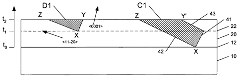
Other defect behavior has been observed. As discussed above, new carrot
defects may originate at the growth interruption/etch step, as illustrated by
defect D1
in Figure 6. In addition, as indicated by defect C1 in Figure 6, the threading
dislocation 41 in the ~0001~ may be converted during the interruption/etch
step into a
basal plane dislocation 43 which propagates in approximately the ~l 120>
direction
resulting in the shape illustrated.
The defect behavior described above in connection with carrot defects Al, B1,
C1 and D1 is illustrated in the micrographs of Figures 7(A), 7(B), 7(C) and
7(D). In
the process illustrated in Figures 7(A)-(D), a layer of silicon carbide was
epitaxially
grown on a bulk substrate off cut at an angle of about eight degrees towards
the
~l 120 direction. After 10 microns of growth, the flow of source gases was
interrupted, and the layers were etched by about one-half micron. Growth of
the
epitaxial layer was resumed, and the layer was grown an additional 30 microns.
The
-12-
CA 02555431 2006-08-08
WO 2005/093137 PCT/US2004/038895
layer was then etched with molten KOH to highlight defects in the material.
Figures
7(A)-(D) are micrograph images of the etched layers.
Figure 7(A) illustrates a carrot defect similar to defect A1 that continued to
propagate through the growth interruption/etch step. The carrot defect
extended a
distance of 243 microns at the surface of the layer.
Figure 7(B) illustrates a carrot defect similar to defect B1 that was
terminated
at the growth interruption/etch step. The carrot defect grew to a width of 62
microns
before termination. It is noteworthy that the KOH etch did not etch a deep
trench
where the morphological remnant of the carrot appears, which indicates that
the
prismatic stacking fault did not propagate to the surface of the epitaxial
layer.
Figure 7(C) illustrates a carrot defect similar to defect C1 that was modified
at the growth interruption/etch step such that the threading dislocation in
the ~0001~
direction was converted to a dislocation propagating in approximately the
~1120~
direction.
Figure 7(D) illustrates a carrot defect similar to defect D1 that originated
at
the growth interruption/etch step.
To examine the efficacy of the process, nearly identical wafers derived from
the same SiC boule ("sister wafers") were processed with and without employing
a
process according to the invention. The carrot defect densities on each of the
wafers
were measured and compared. Since the number of carrot defects in a wafer is
strongly dependent on the boule, it may be useful to compare carrot defect
reduction
in wafers taken from the same boule. For this comparison, the inventors
calculated
the ratio of the number of carrot defects in epilayers grown using the present
invention to the number of carrot defects in epilayers grown without the
invention,
both on sister wafers. In each case, one set of wafers was grown without
growth
interruption/etching/growth cycle, while one set of wafers included an
interruption/etching/growth cycle.
For each growth run, three wafers were loaded into a CVD reactor. The
reactor was heated to growth temperature under a flow of carrier gas (Hz)
only. At a
temperature consistent with an etch-rate of approximately 3 microns/hour,
growth of
silicon carbide was initiated by introduction of silane (SiH4) and propane
(C3Hg)
reactant gases. Appropriate growth temperatures are system dependent and may
be
determined by a skilled person without undue experimentation.
-13-
CA 02555431 2006-08-08
WO 2005/093137 PCT/US2004/038895
In the control experiment, this growth was continued until a silicon carbide
epitaxial layer of approximately 40 microns had been grown. In other
experiments,
growth was initiated in the same manner as the control experiment but was
interrupted
once or twice by stopping the flow of both the silane and propane. During that
interruption of about 12 minutes duration, hydrogen in the carrier gas etched
about 0.6
microns from the previously grown epitaxial layer. At the end of the growth
interruption, silane and propane were reintroduced to resume growing silicon
carbide.
In the first experiment, the initial epitaxial layer was approximately 5
microns
thick, there was a single growth interruption, and the final epitaxial layer
was
approximately 35 microns thick. In the second experiment, the initial
epitaxial layer
was approximately 2.5 microns thick, there was a single growth interruption,
and the
final epitaxial layer was approximately 37.5 microns thick. In the third
experiment,
the initial epitaxial layer was approximately 2.5 microns thick, there were
two growth
interruptions with an additional 2.5 microns thick epitaxial layer between
them, and
the final epitaxial layer was approximately 35 microns thick. After growth,
all of the
carrots on each wafer were counted using a Nomarski microscope. The number of
carrots on each wafer in the experimental runs was counted and compared to the
number of carrots on its sister wafer in the control experiment. For purposes
of the
experiment, carrot defects were counted if they were not terminated within the
epitaxial layer (i.e. if they continued to propagate to the surface). In each
case, there
was significant reduction in the number of carrot defects.
A histogram of the carrot reduction ratio is presented in Figure 8. The
abscissa (x-axis) of Figure 8 represents the ratio of carrot defect densities
in wafers
prepared using a process according to embodiments of the present invention to
wafers
that did not use such a process. The ordinate (y-axis) represents the
percentage of
samples falling within the indicated range of defect reduction Thus, Figure 8
shows
that the majority of wafers grown using the inventive process had only 10 to
30% of
the number of carrot defects found in the control wafers. The median carrot
density
was reduced from 2.76 cm Z to 0.67 cm 2.
As illustrated in Figure 8, by using the process described above, the number
of carrots can be reduced by roughly 70-80% of the expected value.
While the systems and methods have been described in relation to processes
for depositing layers on substrates such as semiconductor wafers, the present
invention may be employed in processes for depositing layers or the like on
other
-14-
CA 02555431 2006-08-08
WO 2005/093137 PCT/US2004/038895
types of substrates. The systems and methods of the present invention may be
particularly useful in processes for forming an epitaxial layer on a
substrate.
Various other modifications may be made in accordance with the invention.
For example, heating systems may be used other than or in addition to
inductive
S heating.
As used herein a "system" may include one or multiple elements or features.
In the claims that follow, the "deposition system", the "deposition control
system", the
"buffer gas supply system", the "process gas supply system" and the like are
not
limited to systems including all of the components, aspects, elements or
features
discussed above or corresponding components, aspects, elements or features.
The foregoing is illustrative of the present invention and is not to be
construed
as limiting thereof. Although a few exemplary embodiments of this invention
have
been described, those skilled in the art will readily appreciate that many
modifications
are possible in the exemplary embodiments without materially departing from
the
novel teachings and advantages of this invention. Accordingly, all such
modifications
are intended to be included within the scope of this invention. Therefore, it
is to be
understood that the foregoing is illustrative of the present invention and is
not to be
construed as limited to the specific embodiments disclosed, and that
modifications to
the disclosed embodiments, as well as other embodiments, are intended to be
included
within the scope of the invention.
-15-