Note: Descriptions are shown in the official language in which they were submitted.
CA 02555813 2006-08-09
WO 2005/081182 PCT/US2005/004640
RFID TAG AND METHOD OF MANUFACTURING THE SAME
BACKGROUND OF THE INVENTION
The present invention relates generally to wireless communication devices and
more particularly to a novel radio frequency identification (RFID) tag and to
a method
of manufacturing said RFID tag.
Current inventory and manufacturing methods rely on the ability to track and
identify items, such as packages, containers, individual parts, inventory
items orother
similar items of concern, and to communicate information relating to said
items in a
wireless manner. One method of tracking and providing information relating to
an
item is to incorporate a wireless communication device, such as an active or
passive
transponder, into an identification tag that responds to wireless
interrogation and
commands and, in turn, to attach said identification tag directly to the item.
The tag
is preferably designed to store or represent pertinent information relating to
the item
to which it is attached, such as a unique identifying number, an expiration
date, a
"born on" date, manufacturing information, shipment status and the like.
A radio frequency identification (RFID) tag is one well-known type of wireless
communication device which transmits and/or receives information relating to
an item
using radio frequency (RF) signals.
One well-known type of RFID tag includes an antenna and an integrated circuit
(IC) chip mounted on the antenna. The aforementioned components are typically
enclosed within a two-piece plastic housing or package. In operation, the IC
chip is
programmed to store pertinent information relating to the item to which the
RFID tag
is secured. In response to an appropriate interrogation signal, the IC chip
converts
said programmed information into a corresponding electromagnetic signal which
is
propagated as radio frequency (RF) waves by the antenna.
Although RFID tags of the type described above are suitable for use on many
different types of items, such tags are not well-suited for use on metallic
items for the
reason that metallic items tend to interfere with the RF signal transmitted by
the RFID
tag antenna.
Accordingly, one approach to remedy this problem has been to provide the
RFID tag with a metallic reflector which makes the RFID tag more tolerant of
nearby
metals while retaining its RF functionality. Specifically, a metallic
reflector is secured
to the outer surface of the plastic package housing the antenna and IC chip.
In use,
1
CA 02555813 2006-08-09
WO 2005/081182 PCT/US2005/004640
the metallic reflector functions as an electrically conductive back plane
which reflects
RF signals transmitted by the RFID tag antenna away from the metal item to
which
the RFID tag is secured. In this respect, the metallic reflector serves to
effectively
insulate the RFID tag from the metal object to which it is secured, which is
highly
desirable.
An example of an RFID tag of the aforementioned type is disclosed in U.S.
Patent No. 6,501,435, inventors King et al., which issued December 31, 2002,
and
which is incorporated herein by reference.
RFID tags having a metallic reflector are commonly manufactured in the
following manner. First, using injection molding, a plastic base and a plastic
cover
for the RFID tag package are separately formed, the base and/or the cover
being
appropriately contoured to matingly receive the RFID tag package. After said
injection molding step, the RFID tag antenna, which is commonly constructed as
a
thin strip of etched copper foil, is secured to the top surface of the plastic
base. It
should be noted that, rather than securing the antenna to the base in a
separate step,
the plastic base may, in the alternative, be injection molded around the
antenna.
Either immediately prior to or immediate afterthe antenna is secured to the
base, the
IC chip for the RFID tag is soldered to the top surface of the antenna. With
the
antenna and IC chip coupled to the base, the plastic cover is then sonic-
welded, by
hand, to the top of the plastic base so as to enclose the antenna and IC chip
therebetween. In a final step, the metallic reflector is secured to the bottom
surface
of the base using an adhesive.
RFID tags manufactured in the method described above suffer from a couple
of notable shortcomings.
One such shortcoming of the foregoing approach is that the molds used to
make the injection molded base and cover are typically only sized for use with
an
antenna (and IC chip) of a particular size. Consequently, if one wishes to
vary the
dimensions of the antenna (e.g., to tune the antenna for different
applications), one
must obtain new molds for manufacturing the base and cover. This is highly
undesirable as molds are quite expensive.
Another shortcoming of the foregoing approach is the low throughput of the
process for manufacturing and assembling the tag. As noted above, each tag is
manufactured, one at a time, using a labor-intensive and time-consuming
process.
2
CA 02555813 2006-08-09
WO 2005/081182 PCT/US2005/004640
SUMMARY OF THE INVENTION
It is an object of the present invention to provide a new radio frequency
identification (RFID) tag and method of manufacturing the same.
It is another object of the present invention to provide an RFID tag and
method
of manufacturing the same that overcome at least some of the shortcomings
associated with existing RFID tags and their methods of being manufactured.
It is yet another object of the present invention to provide an RFID tag and
method of manufacturing the same that is well-suited for mass-production at a
high
rate of throughput.
According to one aspect of the present invention, there is provided a tag
comprising (a) an inlay, said inlay comprising (i) an antenna, and (ii) a
wireless
communication device coupled to said antenna; and (b) a plastic extrudate,
said
plastic extrudate encapsulating said antenna and said wireless communication
device.
According to another aspect of the present invention, there is provided a tag
comprising (a) a plastic casing comprising (i) a bottom member shaped to
define a
longitudinal cavity and (ii) a top member applied to said bottom member to at
least
partially enclose the longitudinal cavity, and (b) an inlay disposed within
the
longitudinal cavity, said inlay comprising, (i) a carrier sheet, (ii) an
antenna disposed
on said carrier sheet, and (iii) a wireless communication device coupled to
said
antenna.
According to yet another aspect of the present invention, there is provided a
method of continuously manufacturing a plurality of tags, each tag comprising
a
plastic extrudate and an inlay surrounded by said plastic extrudate, said
method
comprising the steps of (a) providing a continuous supply of inlays, said
continuous
supply of inlays comprising a continuous carrier web, a plurality of antennae
positioned on said continuous carrier web at spaced intervals and a wireless
communication device coupled to each of said antennae, (b) feeding said
continuous
supply of inlays into a cross-head extruder so as to yield a continuous block
which
includes said continuous supply of inlays surrounded by a plastic extrudate,
and (c)
cutting said continuous block between successive antennae so as to yield
individual
tags.
3
CA 02555813 2006-08-09
WO 2005/081182 PCT/US2005/004640
According to still another aspect of the present invention, there is provided
a
method of continuously manufacturing a plurality of tags, said method
comprising the
steps of (a) providing a single continuous strip which is shaped to include a
continuous longitudinal cavity along its entire length, (b) depositing a
continuous
supply of inlays into the continuous longitudinal cavity, said continuous
supply of
inlays comprising a carrier web, a plurality of antennae disposed on said
carrier web
at spaced intervals, and a wireless communication device coupled to each of
said
antennae, (c) applying a cover over said continuous supply of inlays disposed
within
said single continuous strip, and (d) cutting said cover, said continuous
supply of
inlays and said single continuous strip between successive antennae to yield
individual tags.
According to still yet another aspect of the present invention, there is
provided
a method of continuously manufacturing a plurality of tags, each tag
comprising a
plastic casing and an inlay encased within said plastic casing, said method
comprising the steps of (a) providing a single continuous strip having a
plurality of
cavities at spaced intervals, (b) depositing an inlay within each cavity in
said single
continuous strip, each inlay comprising a carrier sheet, an antenna disposed
on said
carrier sheet and a wireless communication device coupled to said antenna, (c)
applying a single continuous web to said single continuous sheet to enclose
each
inlay within its corresponding cavity, and (d) cutting said single continuous
strip and
said single continuous web between successive cavities to yield individual
tags.
According to a further aspect of the present invention, there is provided a
method of continuously manufacturing a plurality of tags, each tag comprising
a
plastic casing and an inlay encased within said plastic casing, said method
comprising the steps of (a) providing a single continuous member having a
plurality
of cavities at spaced intervals, (b) depositing an inlay within each cavity in
said single
continuous strip, each inlay comprising a carrier sheet, an antenna disposed
on said
carrier sheet and a wireless communication device coupled to said antenna, (c)
applying a plug over each inlay to enclose said inlay within its corresponding
cavity,
and (d) cutting said single continuous strip between successive cavities.
The present invention is also directed to a continuous supply of inlays, said
continuous supply of inlays comprising (a) a continuous web, (b) a plurality
of
antennae disposed on the top surface of said continuous web at spaced
intervals,
4
CA 02555813 2006-08-09
WO 2005/081182 PCT/US2005/004640
and (c) a plurality of wireless communication devices, each wireless
communication
device being coupled to a corresponding antenna.
Various other features and advantages will appear from the description to
follow. In the description, reference is made to the accompanying drawings
which
form a part thereof, and in which is shown by way of illustration, various
embodiments
for practicing the invention. The embodiments will be described in sufficient
detail to
enable those skilled in the art to practice the invention, and it is to be
understood that
other embodiments may be utilized and that structural changes may be made
without
departing from the scope of the invention. The following detailed description
is
therefore, not to be taken in a limiting sense, and the scope of the present
invention
is best defined by the appended claims.
5
CA 02555813 2006-08-09
WO 2005/081182 PCT/US2005/004640
BRIEF DESCRIPTION OF THE DRAWINGS
In the drawings wherein like reference numerals represent like parts:
Fig. 1 is a perspective view of a first embodiment of a radio frequency
identification (RFID) tag constructed according to the teachings of the
present
invention, said tag being broken away in part to more clearly show the carrier
sheet
and antenna of the RF inlay;
Fig. 2 is a longitudinal section view of the RFID tag shown in Fig. 1;
Fig. 3 is an enlarged, fragmentary, top plan view of the RF inlay antenna
shown in Fig. 2, the RF inlay being shown with the wireless communication
device
removed therefrom;
Fig. 4 is a fragmentary, simplified, schematic view of an automated method for
continuously manufacturing a supply of the RFID tags shown in Fig.1;
Fig. 5 is a perspective view of a second embodiment of an RFID tag
constructed according to the teachings of the present invention;
Fig. 6 is a longitudinal section view of the RFID tag shown in Fig. 5;
Fig. 7 is a simplified schematic view of an automated method for continuously
manufacturing a supply of the RFID tags shown in Fig. 5;
Fig. 8 is a perspective view of a third embodiment of an RFID tag constructed
according to the teachings of the present invention, said tag being broken
away in
part to more clearly show the carrier sheet and antenna of the RF inlay;
Fig. 9 is a longitudinal section view of the RFID tag shown in Fig. 8;
Fig. 10 is a perspective view of a fourth embodiment of an RFID tag
constructed according to the teachings of the present invention, said tag
being
broken away in part to more clearly show the carrier sheet and antenna of the
RF
inlay;
Fig.11 is a simplified schematic view, shown partly in section, of an
automated
method for continuously manufacturing a supply of the RFID tags shown in Fig.
10;
Fig. 12 is a perspective view of a fifth embodiment of an RFID tag constructed
according to the teachings of the present invention, the bottom member of said
tag
being broken away in part to more clearly show the carrier sheet and antenna
of the
RF inlay;
Fig. 13 is a longitudinal section view of the RFID tag shown in Fig. 12; and
6
CA 02555813 2006-08-09
WO 2005/081182 PCT/US2005/004640
Fig. 14 is a longitudinal section view of a sixth embodiment of an RFID tag
constructed according to the teachings of the present invention.
7
CA 02555813 2006-08-09
WO 2005/081182 PCT/US2005/004640
DETAILED DESCRIPTION OF THE PREFERRED EMBODIMENT
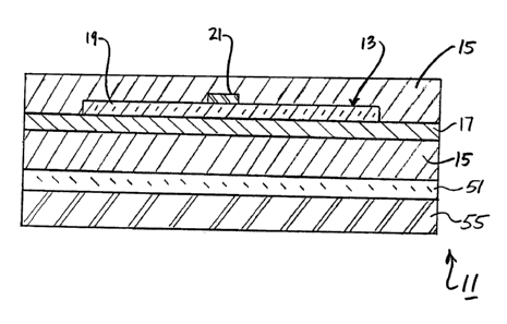
Referring now to Figs. 1 and 2, there are shown perspective and section
views, respectively, of a first embodiment of a radio frequency identification
(RFID)
tag constructed according to the teachings of the present invention and
identified
generally by reference numeral 11. In operation, RFID tag 11 is designed to be
affixed onto a particular item (or packaging therefor) and, in response to an
active or
passive radio frequency signal, wirelessly transmit information relating to
said item.
RFID tag 11 comprises a radio frequency (RF) inlay 13 and a plastic extrudate
15, extrudate 15 surrounding or enveloping inlay 13 in the manner to be
described
below.
RF inlay 13 includes a carrier sheet 17, an antenna 19 formed on carrier sheet
17 and a wireless communication device 21 mounted on antenna 19.
Carrier sheet 17 preferably comprises a heat-stable polymeric film having a
thickness in the range of about 2 mm to 5 mm. Examples of materials suitable
for
use as carrier sheet 17 include, but are not limited to, polyester films,
polyethylene
terephthalate (PET) films and polyimide films (such as Kapton~ polyimide film,
which
is commercially available from E.I. DuPont de Nemours and Company Corporation,
Wilmington, DE). Carrier sheet 17 is preferably manufactured as a continuous
web
which can be wound into roll form, as will be described further below.
Antenna 19 preferably comprises a conductive material (e.g., copper or silver)
of appropriate size and 'shape, which is printed directly onto the top surface
of carrier
sheet 17. Preferably, antenna 19 is formed by depositing a layer of the
conductive
material onto carrier sheet 17, laying a template over the layer of conductive
material
and then etching away portions of the conductive material (e.g., using an acid
bath)
in order to leave remaining the desired shape of antenna 19. Alternatively,
antenna
19 may be formed by printing a conductive ink in a desired pattern directly
onto
carrier sheet 17.
Referring now to Fig. 3, there is shown an enlarged, fragmentary, top plan
view of antenna 19 printed on carrier sheet 17. Antenna 19 is preferably in
the form
of a bilaterally symmetrical dipole antenna which includes first and second
conductive
tabs 23 and 25, respectively, which are substantially identical in shape.
First
conductive tab 23 includes a first end 27 and a second end 29. Similarly,
second
conductive tab 25 includes a first end 31 and a second end 33. Tabs 23 and 25
are
8
CA 02555813 2006-08-09
WO 2005/081182 PCT/US2005/004640
linearly arranged in an end-to-end relationship with first end 27 of first tab
23 and
second end 33 of second tab 25 spaced slightly apart from one another. A
small,
square-shaped conductive pad 35 is disposed in proximity to, but spaced apart
from,
first end 27 of first tab 23 and second end 33 of second tab 25. Together,
first end
27 of first tab 23, second end 33 of second tab 25 and pad 35 define a landing
area
37 on which wireless communication device 21 is conductively bonded. Antenna
19
further comprises a pair of arcuate inductors 39 and 41 which connect first
tab 23 to
second tab 25, inductors 39 and 41 being disposed on opposite sides of landing
area
35. In operation, inductors 39 and 41 create a level of inductance across the
wireless
communication device 21 bonded to landing area 35, thereby enabling the
wireless
communication device 21 to operate at its peak performance.
Additional information pertaining to antenna 19 may be found in one or more
of the following commonly-assigned U.S. patent applications, all of which are
incorporated herein by reference: U.S. Patent Application Serial No.
10/410,252,
inventor Forster, filed April 10, 2003; U.S. Provisional Patent Application
Serial No.
60/517,148, inventors Power et al., filed November 4, 2003; and U.S.
Provisional
Patent Application Serial No. 60/517,156, inventors Power et al., filed
November 4,
2003.
It should be understood that, although, in the present embodiment, antenna
19 is preferably a straight, center-fed, one-half wavelength, symmetric,
dipole
antenna, antenna 19 could be replaced with other types of antennae, such as
conventional antennae (e.g., a monopole antenna), without departing from the
spirit
of the present invention.
Wireless communication device 21 is preferably in the form of an integrated
circuit (IC) chip which is mounted on antenna 19. Wireless communication
device 21
is conductively bonded to landing surface 37 of antenna 19 by any conventional
means, such as through a soldering process or through the use of a conductive
adhesive. In this manner, a conductive path is established between wireless
communication device 21 and antenna 19.
Wireless communication device 21 represents any conventional device which,
in response to an active or passive radio frequency signal, wirelessly
transmits
information relating to the particular item to which RFID tag 11 is affixed.
Preferably,
9
CA 02555813 2006-08-09
WO 2005/081182 PCT/US2005/004640
wireless communication device 21 is capable of transmitting signals at
multiple
resonant frequencies.
As noted above, carrier sheet 17 is preferably manufactured as an elongated
web, which enables a plurality of RF inlays 13 to be constructed using a
common
sheet 17. Specifically, a plurality of antennae 19 are preferably printed on
carrier
sheet 17 at spaced intervals (e.g., between 1 /4 inch and 1 /2 inch apart),
each
antenna 19 having a corresponding wireless communication device 21 mounted
thereon. In this manner, a plurality of interconnected RF inlays 13 may be
created
which may then, in turn, be wound into an RF inlay supply roll.
Referring now to Fig. 4, there is shown a simplified schematic representation
of an automated method for continuously manufacturing a supply of RFID tags
11.
In the manufacturing process, a plurality of interconnected inlays 13 in the
form of an
RF inlay supply roll 43 are introduced from a reel 44 into a cross-head
extruder 45.
Specifically, cross-head extruder 45 is equipped with a die head 47, die head
47
being provided with a slot (not shown). RF inlay supply roll 43 is fed
directly into die
head 47 through the aforementioned slot. As extruder 45 generates heat, resin
previously deposited into extruder 45 in pellet form begins to melt. The
molten plastic
in turn coaxially surrounds or envelopes the portion of supply roll 43 which
has been
introduced into die head 47. Extruder 45 then forces the molten thermoplastic
material out through die head 47 in a linear fashion to yield a continuously
extruded
block 49, block 49 comprising plastic extrudate 15 and supply roll 43, with
antenna
19 and wireless communication device 21 of each RF inlay 13 being encapsulated
on all sides within extrudate 15. Continuous block 49 is preferably
transported away
from cross-head extruder 45 by means of a linear conveyor belt (not shown).
It should be noted that plastic extrudate 15 preferably comprises a durable,
thermoplastic material including, but not limited to, a rigid polyvinyl
chloride (PVC),
a polyester, a polycarbonate, a polyethylene or a polypropylene, which can be
molded into a rectangular block shape.
After the extrusion process, a metallic reflector 51 is laminated onto the
bottom
surface of block 49, preferably using a heat-activatable adhesive. The purpose
of
metallic reflector 51 is to reflect RF signals generated by RF inlay 13 away
from a
metallic item to which RFID tag 11 is secured, thereby effectively insulating
RF inlay
13 from the metallic item. Examples of suitable metals for use as metallic
reflector
CA 02555813 2006-08-09
WO 2005/081182 PCT/US2005/004640
51 include aluminum and/or copper. Preferably, metallic reflector 51 is
manufactured
as a continuous sheet or strip of metal, said continuous strip being wound
onto a
supply reel 53. In this manner, metallic reflector 51 can be continuously
unwound
from supply reel 53 and laminated to the underside of block of thermoplastic
material
49 to allow for the continuous assembly of RFID tags 11.
It should be noted that the application of metallic reflector 51 to the
underside
of block 49 is optional and is only preferred when the item to which RFID tag
11 is to
be secured is metallic in nature. As a result, metallic reflector 51 could be
eliminated
entirely from the assembly process.
It should be noted that, by modifying extruder die head 47 to include a second
slot, metallic reflector 51 may also be fed into die head 47 and
simultaneously
surrounded within plastic extrudate 15 with inlay 13 during the extrusion
process.
After lamination of metallic reflector 51 onto block 49, the resulting
laminate
is preferably advanced to a cooling station (not shown). At the cooling
station, the
laminate is passed through a water bath (not shown) approximately 15-20 feet
long
in order to fix, or set, the shape of plastic extrudate 15.
A mounting adhesive 55 may be laminated onto the bottom surface of metallic
reflector 51 so that tag 11 may be adhesively mounted onto a desired article.
Preferably, adhesive 55 is manufactured as a continuous sheet or strip, said
continuous strip being wound onto a supply reel 57. In this manner, adhesive
55 can
be continuously unwound from reel 57 and secured to the underside of metallic
reflector 51.
It should be noted that, where it is not necessary or desirable to adhesively
mount tag 11 onto an article, adhesive 55 is not needed and the application of
mounting adhesive 55 onto the underside of metallic reflector 51 may be
eliminated
from the assembly process.
In the final step of the assembly process, continuous block 49 (along with any
reflectors 51 and adhesives 55 affixed thereto) is cut, as required, to form
the
individual RFID tags 11. It should be noted that sensors (not shown) may be
positioned along the linear conveyor belt to locate antennae 19 within block
49 so
that block 49 may be cut between adjacent antennae 19, as opposed to being cut
within an antenna 19. Individual RFID tags 11 severed from block 49 can be
packaged and/or shipped, as deemed necessary. The cut edges could be sealed
11
CA 02555813 2006-08-09
WO 2005/081182 PCT/US2005/004640
using techniques, such as heat-crimping, application of a sealant or
application of a
suitable solvent.
It should be noted that, in an optional step prior to said cutting step,
continuous
block 49 (along with any reflectors 51 and adhesives 55 affixed thereto) may
be
crimped between adjacent antennae 19.
Without wishing to limit the invention in any conceivable way to any
particular
embodiment of the invention, the present inventors hereby disclose the
following
preferred dimensions of RFID tag 11: RFID tag 11 preferably has a height H
(excluding adhesive 55) of approximately 5 mm, a length L of approximately 150
mm,
and a width W of approximately 22 mm.
It should be noted that numerous variations could be made to RFID tag 11
(and its corresponding assembly process) without departing from the spirit of
the
present invention.
As an example, referring now to Figs. 5 and 6, there are shown perspective
and section views, respectively, of a second embodiment of a radio frequency
identification (RFID) tag constructed according to the teachings of the
present
invention and identified generally by reference numeral 111.
RFID tag 111 is similar to RFID tag 11 in that RFID tag 111 includes a radio
frequency (RF) inlay 113 which is identical to RF inlay 13. Specifically, RF
inlay 113
comprises an elongated carrier sheet 117 preferably manufactured as a
continuous
web of heat-stable polymeric film, an antenna 119 printed directly onto the
top
surface of carrier sheet 117 and a wireless communication device 121
conductively
bonded to antenna 119.
However, RFID tag 111 differs from RFID tag 11 in that RF inlay 113 is
positioned within a two-piece plastic casing 115 whereas RF inlay 13 is
positioned
within a unitary plastic extrudate 15.
Specifically, casing 115 includes an elongated bottom member 123 which is
manufactured out of plastic. Bottom member 123 is preferably shaped to have a
corrugated type of construction, bottom member 123 being U-shaped in lateral
cross-
section along its length so as to define a longitudinal rectangular cavity 125
therewithin. It should be noted that bottom member 123 is uniform in cross-
section
with cavity 125 extending its entire length. Preferably, bottom member 123 is
formed
in one step through an extrusion process.
12
CA 02555813 2006-08-09
WO 2005/081182 PCT/US2005/004640
Cavity 125 is sized and shaped to receive RF inlay 113. After RF inlay 113
has been placed within cavity 125 of bottom member 123, an elongated top
member
127 is applied to bottom member 123 so as to substantially enclose
longitudinal
cavity 125 along its length with antenna 119 and wireless communication device
121
positioned therewithin. (It should be noted that a small space or air gap
exists
between inlay 113 and top member 127.) Top member 127 is preferably formed
through an extrusion process.
In order to fully enclose antenna 119 and wireless communication device 121
within longitudinal cavity 125, the free ends of two-piece casing 115 are
preferably
crimped. However, it should be noted that casing 115 is not represented in the
drawings as being crimped at its ends for simplicity purposes only.
Like RFID tag 11, RFID tag 111 may include a metallic reflector 151 which is
laminated onto the underside of bottom member 123 and/ora mounting adhesive
155
which is laminated onto the underside of metallic reflector 151. It should be
noted
that the application of metallic reflector 151 to the underside of bottom
member 123
is optional and is only preferred when the item to which RFID tag 111 is to be
secured is metallic in nature. Furthermore, it should be noted that, where it
is not
necessary or desirable to adhesively mount tag 111 onto an article, adhesive
155 is
not needed and the application of mounting adhesive 155 onto the underside of
metallic reflector 151 may be eliminated from the assembly process.
Referring now to Fig. 7, there is shown a simplified schematic representation
of an automated method for continuously manufacturing a supply of RFID tags
111.
For simplicity purposes only, the continuous supply of RFID tags 111 is shown
without metallic reflector 151 and adhesive 155. However, it is to be
understood that
metallic reflector 151 and adhesive 155 could be introduced into the automated
process in the same manner in which reflector 51 and adhesive 55 were
introduced
into the above-described method of manufacturing RFID tags 11.
In the process for manufacturing RFID tags 111, an extruder 157 generates
a continuous extrudate strip 159 which has a uniform, U-shaped lateral cross-
section
along its length. As a result, continuous strip 159 defines a continuous
longitudinal
cavity 161. It should be noted that continuous strip 159 can be cut (in a
later step to
be described further below) to generate a plurality of bottom members 123. A
plurality
13
CA 02555813 2006-08-09
WO 2005/081182 PCT/US2005/004640
of interconnected inlays 113 produced in the form of an RF inlay supply roll
163 are
introduced from a reel 165 into elongated cavity 161.
With the plurality of interconnected inlays 113 deposited in-line within
cavity
161, a secondary extruder 167 generates a continuous plastic web 169 which is
applied in-line to the top of strip 159. It should be noted that web 169 can
be cut (in
a later step to be described further below) to generate a plurality of top
members 127.
Web 169 is brought together with continuous strip 159 to substantially enclose
interconnected RF inlays 113 within cavity 161.
It should be noted that web 169 may be affixed to strip 159 using any one of
a variety of different methods. As an example, web 169 may be hot when applied
to
strip 159 to promote the adhesion therebetween. As another example, web 169
may
be cool when initially applied to strip 159 but then subsequently heated after
said
application step to promote the adhesion therebetween. As another example, web
169 may be affixed to strip 159 using a conventional adhesive.
In the final steps of the assembly process, the continuous strip 159 and web
169 (along with any reflectors 151 and adhesives 155 affixed thereto) are
crimped
between adjacent antennae 119 to fully enclose each antenna 119 and wireless
communication device 121 within cavity 161. After the crimping process, the
continuous strip 159 and web 169 (along with any reflectors 151 and adhesives
155
affixed thereto) are cut between adjacent antennae 119 to form the individual
RFID
tags 111. Sensors (not shown) located along the continuous assembly line may
be
used to locate antennae 119 within cavity 161 during the crimping and cutting
processes.
It should be noted that, although the process for fabricating tag 111 as
described above includes, among other things, affixing web 169 to strip 159
and then
cutting the resulting assembly into individual tags, one could first cut strip
159 and
web 169 into respective pluralities of individual bottom members 123 and
individual
top members 127 and then affix the individual top members 127 to the
individual
bottom members 123.
Referring now to Figs. 8 and 9, there are shown perspective and section
views, respectively, of a third embodiment of a radio frequency identification
(RFID)
tag constructed according to the teachings of the present invention and
identified
generally by reference numeral 171.
14
CA 02555813 2006-08-09
WO 2005/081182 PCT/US2005/004640
Tag 171 is similar in most respects to tag 111, the principal difference
between
the two tags being that tag 171 does not include a top member 127. Instead,
tag 171
includes a plug 177, plug 177 being positioned directly on top of inlay 113
and
occupying some or all of the remaining space of cavity 125 of bottom member
123.
Accordingly, as can readily be appreciated, tag 171 does not possess an airgap
over
inlay 113 of the type described above in connection with tag 111.
Plug 177 may be formed, for example, by extruding molten plastic over inlay
113 until cavity 125 is partially or completely filled and then allowing the
molten
plastic to cool and harden in place. Alternatively, plug 177 may be formed by
pouring
into cavity 125 a suitable non-molten polymer and causing or allowing such a
polymer
to solidify in place. Examples of such polymers include (i) emulsion-based or
solvent-
borne polymers and (ii) curable polymers including, but not limited to, two-
part
polymers (such as two-part epoxies), photo-curable polymers, and air-curable
polymers.
It should be noted that plug 177 may be formed prior to the cutting of strip
159
into individual bottom members 123 or after the cutting of strip 159 into
individual
bottom members 123.
Referring now to Fig. 10, there is shown a perspective view of a fourth
embodiment of a radio frequency identification (RFID) tag constructed
according to
the teachings of the present invention, said RFID tag being identified
generally by
reference numeral 181.
Tag 181 is similar in most respects to tag 111, the principal difference
between
the two tags being that tag 181 does not include a trough-shaped bottom member
123, but rather, includes a rectangular prismatic bottom member 183, inlay 113
being
sandwiched between bottom member 183 and top member 127.
Referring now to Fig.11, there is shown a simplified schematic representation,
partly in section, of an automated method for continuously manufacturing a
supply
of RFID tags 181. For simplicity purposes only, the continuous supply of RFID
tags
181 is shown without metallic reflector 151 and adhesive 155. However, it is
to be
understood that metallic reflector 151 and adhesive 155 could be introduced
into the
automated process in the same manner in which reflector 51 and adhesive 55
were
introduced into the above-described method of manufacturing RFID tags 11.
CA 02555813 2006-08-09
WO 2005/081182 PCT/US2005/004640
In the process for manufacturing RFID tags 181, an extruder 185 generates
a continuous extrudate 186 in the form of a rectangular block. A plurality of
interconnected inlays 113 manufactured in the form of an RF inlay supply roll
163 are
unwound from a reel 165 and laid on top of extrudate block 186.
With the plurality of interconnected inlays 113 deposited on top of extrudate
block 186, a secondary extruder 187 generates a continuous plastic web 189
which
is applied in-line over the interconnected inlays 113 and any exposed areas on
top
of extrudate block 186. In this manner, web 189 and extrudate block 186
cooperatively surround interconnected RF inlays 113.
It should be noted that web 189 may be affixed to extrudate block 186 using
any one of a variety of different methods. As an example, web 189 may be hot
when
applied to extrudate block 186 to promote the adhesion therebetween. As
another
example, web 189 may be cool when initially applied to extrudate block 186 but
then
subsequently heated after said application step to promote the adhesion
therebetween. As another example, web 189 may be affixed to extrudate block
186
using a conventional adhesive.
In the final steps of the assembly process, extrudate block 186 and web 189
(along with any reflectors 151 and adhesives 155 affixed thereto) are crimped
between adjacent antennae 119 to fully enclose each antenna 119 and wireless
communication device 121 between extrudate block 186 and web 189. After the
crimping process, extrudate block 186 and web 189 (along with any reflectors
151
and adhesives 155 affixed thereto) are cut between adjacent antennae 119 to
form
the individual RFID tags 181. Sensors (not shown) located along the continuous
assembly line may be used to locate antennae 119 during the crimping and
cutting
processes.
It should be noted that, although the process for fabricating tag 111 as
described above includes, among other things, affixing web 189 to extrudate
block
186 and then cutting the resulting assembly into individual tags, one could
first cut
block 186 and web 189 into respective pluralities of individual bottom members
183
and individual top members 127 and then affix the individual top members 127
to the
individual bottom members 183.
Referring now to Figs. 12 and 13, there are shown perspective and section
views, respectively, of a fourth embodiment of a radio frequency
identification (RFID)
16
CA 02555813 2006-08-09
WO 2005/081182 PCT/US2005/004640
tag constructed according to the teachings of the present invention and
identified
generally by reference numeral 211.
RFID tag 211 is similar in construction to RFID tag 111 in that RFID tag 211
comprises a radio frequency (RF) inlay 213 which is enclosed within a two-
piece
plastic casing 215.
RF inlay 213 is similar in construction to RF inlay 113 in that RF inlay 213
comprises a carrier sheet 217 preferably manufactured as a web of heat-stable
polymeric film, an antenna 219 printed directly onto the top surface of
carrier sheet
217 and a wireless communication device 221 conductively bonded to antenna
219.
Two-piece plastic casing 215 is similar in construction to casing 115 in that
two-piece plastic casing 215 comprises a bottom member 223 shaped to define a
cavity 225 and a top member 227 affixed to bottom member 223 over cavity 225.
It
should be noted that cavity 225 of bottom member 223 is sized and shaped to
receive an individual RF inlay 213.
Two-piece plastic casing 215 differs from casing 115 in that bottom member
223 has a different shape that bottom member 113. Specifically, bottom member
223
is shaped such that cavity 225 extends only a portion of its length. More
specifically,
cavity 225 does not extend to either of the free ends of bottom member 223.
Rather,
cavity 225 only extends within the middle section of the length of bottom
member
223. Due to the particular construction of bottom member 223, the securement
of top
member 227 onto bottom member 223 serves to completely enclose cavity 225
(with
an RF inlay 213 disposed therein).
RFID tag 211 is similar to RFID tag 111 in that RFID tag 211 includes a
metallic reflector 251 which is laminated onto the underside of bottom member
223
and a mounting adhesive 255 which is laminated onto the underside of metallic
reflector 251. It should be noted that the application of metallic reflector
251 to the
underside of bottom member 223 is optional and is only preferred when the item
to
which RFID tag 211 is to be secured is metallic in nature. Furthermore, it
should be
noted that, where it is not necessary of desirable to adhesively mount tag 211
onto
an article, adhesive 255 is not needed and the lamination of mounting adhesive
255
onto the underside of metallic reflector 251 may be eliminated from the
assembly
process.
17
CA 02555813 2006-08-09
WO 2005/081182 PCT/US2005/004640
An automated method for continuously manufacturing a supply of RFID tags
211 may be accomplished in the following manner. An extruder generates a
continuous extrudate strip which is substantially flat. In a subsequent
thermoforming
process, the continuous strip is provided with a plurality of equidistantly
spaced,
downwardly protruding projections, each projection being shaped to define a
corresponding cavity 225. In this respect, the thermoforming process serves to
provide the continuous strip with an egg-crate-type of construction.
After said thermoforming process, an individual RF inlay 213 is deposited in-
line, by hand or machine, into an associated cavity 225 in the continuous
strip. It
should be noted that the supply of individual RF inlays 213 can be mass
produced
by printing a plurality of antennae 219 on a continuous web at spaced
intervals,
soldering a wireless communication device 221 onto each antenna 219 and
cutting
the continuous web between successive antennae 219 to define the individual RF
inlays 213.
After said deposition step, a secondary extruder generates a continuous
plastic web which is applied in-line to the top of the continuous strip. It
should be
noted that, by applying the plastic web onto the continuous strip, each cavity
225
becomes completely enclosed by casing 215. In this respect, each individual RF
inlay 213 becomes encased on all sides within plastic casing 215.
It should be noted that the plastic web may be affixed to continuous strip
using
any one of variety of different methods. As an example, the plastic web may be
hot
when applied to the continuous strip to promote the adhesion therebetween. As
another example, the plastic web may be cool when initially applied to the
continuous
strip but then subsequently heated after said application step to promote the
adhesion therebetween. As another example, the plastic web may be affixed to
the
continuous strip using a conventional adhesive.
After said application step, the continuous strip and the plastic web are
crimped (as deemed necessary) and cut between successive protrusions formed in
the continuous strip to form the supply of individual RFID tags 211.
It should be noted that metallic reflector 251 and/or adhesive 255, if
required,
could be laminated (directly or indirectly) onto bottom member 223 prior to
said
cutting step (in a similar manner in which reflector 51 and adhesive 55 are
18
CA 02555813 2006-08-09
WO 2005/081182 PCT/US2005/004640
continuously in-line laminated onto extrudate 15) or after said cutting step
(e.g.,
through manual application).
It should also be noted that, although the process for fabricating tag 211 as
described above includes, among other things, affixing the web of top members
227
to the strip of bottom members 223 and then cutting the resulting assembly
into
individual tags, one could first cut the web of top members 227 and the strip
of
bottom members 223 into respective pluralities of individual top members 227
and
individual bottom members 223 and then affix the individual top members 227 to
the
individual bottom members 223.
Referring now to Figs. 14, there is shown a section view of a fifth embodiment
of a radio frequency identification (RFID) tag constructed according to the
teachings
of the present invention and identified generally by reference numeral 311.
Tag 311 is similar in many respects to tag 211, the principal differences
between the two tags being that tag 311 has a bottom member 312, instead of
bottom member 223, and that tag 311 includes a plug 313, instead of top member
227. Plug 313 is positioned directly on top of inlay 213 and occupies some or
all of
the remaining space within bottom member 312. Plug 313 is similar in
composition
to plug 177 of tag 171 and may be formed in the same manner as plug 177.
It should be noted that individual members 312 may be formed by cutting a
strip of interconnected bottom members 312 and that plug 313 may be formed
prior
to the cutting of said strip of interconnected bottom members 312 into
individual
bottom members 312 or after the cutting of said strip of interconnected bottom
members 312 into individual bottom members 312.
The embodiments shown in the present invention are intended to be merely
exemplary and those skilled in the art shall be able to make numerous
variations and
modifications to it without departing from the spirit of the present
invention. All such
variations and modifications are intended to be within the scope of the
present
invention as defined in the appended claims.
19