Note: Descriptions are shown in the official language in which they were submitted.
=CA 02556066 2006-08-10
1
DESCRIPTION
VAPOR PHASE GROWTH APPARATUS
Technical Field
[0001] The present invention relates to a vapor phase
growth apparatus which performs vapor phase growth of a
thin film such as compound semiconductor on a wafer surface
by supplying raw material gas in an high-temperature
environment while heating the wafer, and particularly to a
technology for achieving a uniform in-plane temperature
distribution of a wafer.
Background Art
[0002] Vapor phase growth is employed in various areas
of the industry world today. Needless to say, it is
required for this vapor phase growth that a thin film grown
on a wafer has a uniform thickness, composition, and doping
concentration throughout the plane thereof. In order to
unformalize in-plane film thickness and the like, various
possible methods to be used are considered. Among them, a
technology to achieve uniform temperature of a wafer when
the wafer is heated, is the most important factor.
[0003] FIG. 5 is a cross-sectional view showing a
construction example of a typical conventional vapor phase
growth apparatus. As shown in FIG. 5, a vapor phase growth
apparatus 100 includes a reactor 1, a wafer holder 3 on
=
CA 02556066 2006-08-10
2
which wafers 2 are placed, a susceptor 4 on which the wafer
holder 3 is mounted, a heater 5 provided below the
susceptor 4, a rotation mechanism 6 which rotatably
supports the wafer holder 3 and the susceptor 4, gas inlet
pipes 7 through which raw material gas or carrier gas is
supplied, a gas exhaust pipe 8 through which unreacted gas
is exhausted, and the like.
[0004] FIG. 6 is enlarged views showing construction
of the wafer holder 3 in detail; (a) is a plan view, and
(b) is a cross-sectional view taken along the line A-A of
(a). On one side of the wafer holder 3, a plurality (6 in
FIG. 6) of circular pocket holes 3a are formed along the
same circumference, in which wafers 2 are placed, and on
the other side, the wafer holder 3 is in contact with the
susceptor 4.
[0005] Note that the susceptor 4 is made of a material
having high thermal conductivity (for example, molybdenum
and the like) in order to transfer heat from the heater 5
uniformly. It is also typical to use graphite or
molybdenum having high thermal conductivity, for the wafer
holder 3.
[0006] In the vapor phase growth apparatus having the
above construction, by heating the bottom of the susceptor
4 using the heater 5, heat is transferred to the wafers 2
via the susceptor 4 and the wafer holder 3 so that the
wafers 2 reach a predetermined temperature. In addition,
CA 02556066 2006-08-10
3
by rotating the susceptor 4 at a predetermined rotating
speed using the rotation mechanism 6, vapor phase growth of
a thin film is performed while supplying raw material gas
and carrier gas that has been introduced from the gas
inlets 7 onto the surfaces of the wafers 2 uniformly.
[0007] Further, in FIGS. 5 and 6, the wafer holder 3
on which the wafers 2 are mounted is made from a single
member. However, when a plurality of wafers are mounted,
there is a proposed vapor phase growth apparatus in which a
plurality of wafer holders are provided to correspond to a
plurality of wafers mounted thereon, and the plurality of
wafer holders are mounted on predetermined positions of a
susceptor. (For example, see Patent Document 1).
Patent Document 1: Japanese Patent Laid-Open Publication No.
Heisei 11-8119
Disclosure of the Invention
Problem to be Solved by the Invention
[0008] However, it has been found that, in the above-
mentioned vapor phase growth apparatus 100, the in-plane
temperature distribution of the surface of the entire wafer
holder 3 including the wafers 2, which is parallel with the
wafers 2, is greatly irregular. In addition, when a
temperature distribution of the wafer holder itself was
investigated, it was found that the central portion of the
surface of the wafer holder has higher temperature than the
edge portion thereof (by 15 C or more, for example).
CA 02556066 2006-08-10
4
[0009] It is considered that this temperature
difference is caused by a heating method and installed
position of the heater 5, or differences in thermal
conductivity (thermal diffusivity) among the susceptor 4,
the wafer holder 3 and wafers 2, and contact thermal
resistance thereof. In other words, the contacts between
solid bodies such as between the susceptor 4 and the wafer
holder 3, between the wafer holder 3 and the wafers 2, are
not complete surface contacts but discontinuous surface
contacts (aggregation of point contacts). Therefore, it is
considered that thermal resistance in each border surface
becomes irregular, and the temperature distribution of the
wafer holder 3 (including the wafers 2) is deteriorated.
As a result, in the conventional vapor phase growth
apparatus, the in-plane temperature distribution of each
wafer 2 becomes uneven, and it has thus been difficult to
perform vapor phase growth of a thin film with excellent
uniformity throughout the surface of the wafer 2.
[0010] The present invention has been accomplished to
solve the above problem, and an object of the present
invention is to provide a vapor phase growth apparatus
which can perform vapor phase growth of a thin film with
good uniformity throughout a surface of a wafer by
improving an in-plane temperature distribution of a wafer.
Means for Solving the Problem
[0011] According to the present invention, the vapor
CA 02556066 2006-08-10
phase growth apparatus includes at least a sealable reactor,
a wafer containing member (wafer holder) installed within
the reactor and having a wafer mounting portion (pocket
hole) on a surface thereof for holding a wafer, a gas
supply member (gas inlet pipe) for supplying raw material
gas towards the wafer, a heating member (heater) for
heating the wafer, and a heat uniformizing member
(susceptor) for holding the wafer containing member and
uniformizing heat from the heating member, wherein raw
material gas is supplied into the reactor in a high
temperature environment while heating the wafer by using
the heating member via the heat uniformizing member and the
wafer containing member, to form a film grown on a surface
of the wafer, and wherein a recess portion depressed in a
dome shape is formed at a back side of the wafer containing
member.
[0012] Thus, a space filled with gas having low heat
conductivity is formed between the wafer containing member
and the heat uniformizing member, and the larger the space
becomes, that is, the closer to the central portion of the
dome-shaped recess portion (the central portion of the
wafer containing member), the lower the heat transmission
efficiency becomes. Therefore, temperature was higher at
the central portion than the rest of the areas in a
conventional wafer containing member, however, by the wafer
containing member of the present invention, a temperature
CA 02556066 2006-08-10
6
difference between the central portion and the edge portion
can be reduced.
[0013] Further, when a height and a diameter of the
recess portion provided in the wafer containing member are
represented by H and D, respectively, a ratio of the height
and the diameter HID is between 0.01 and 2.00%. More
preferably, the ratio of the height and the diameter H/D of
the dome-shaped recess portion is between 0.50 and 1.50%.
Thus, a temperature difference between the central portion
and the edge portion on the surface of the wafer containing
member can be reduced to 10 00 or smaller.
[0014] Moreover, it is preferred that the height H of
the dome-shaped recess portion provided in the wafer
containing member be between 0.01 and 3.00 mm. Accordingly,
because a space formed by the dome-shaped recess portion is
limited, it is possible to minimize a reduction of heat
transmission efficiency due to the space.
Effect of the Invention
[0015] According to the present invention, since the
recess portion depressed in a dome shape is formed at the
back side of the wafer containing member, a temperature
difference between the central portion and the edge portion
of the wafer containing member becomes small, and heat is
transmitted evenly to a wafer mounted on the wafer
containing member. As a result, because the temperature
throughout the entire surface of the wafer becomes uniform,
CA 02556066 2012-12-20
7
an effect that vapor phase growth of a thin film having a
good uniformity is realized, can be obtained.
[0015a] In one aspect of the present invention, there is
provided a vapor phase growth apparatus comprising at least a
sealable reactor, a wafer containing member installed within
the reactor and having a wafer mounting portion on a surface
thereof for holding a wafer, a gas supply member for
supplying raw material gas towards the wafer, a heating
member for heating the wafer, and a heat uniformizing member
for holding the wafer containing member and uniformizing heat
from the heating member, the heating uniformizing member
having approximately the same size as the wafer containing
member, and wherein raw material gas is supplied into the
reactor in a high temperature environment while heating the
wafer by using the heating member via the heat uniformizing
member and the wafer containing member, to form a film grown
on a surface of the wafer, wherein a recess portion depressed
in a dome shape is formed at a back side of the wafer
containing member, and the recess portion is formed so that
an apex of the dome shape is arranged on a straight line
connecting a center of the wafer containing member, a center
of the heating uniformizing member and a center of a rotation
mechanism.
CA 02556066 2012-12-20
7a
Brief Description of the Drawings
[0016] [FIG. 1] This is a cross-sectional view
schematically showing a construction of a vapor phase growth
apparatus according to an embodiment.
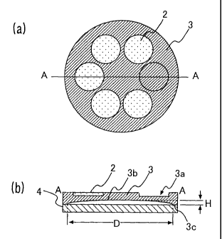
[FIG. 2] These are enlarged views showing a
construction of a wafer holder 3 of the embodiment in detail,
(a) is a top view thereof, and (b) is a cross sectional view
thereof.
[FIG. 3] This is a graph showing a relation between
a height H (mm) of a dome-shaped recess portion 3b formed in
the wafer holder 3, and a temperature difference ,LT ( C) on a
surface of the wafer holder.
[FIG. 4] This is a graph showing a relation between
a ratio H/D of the height and the diameter of the dome-shaped
recess portion 3b, and a temperature difference LT ( C) on a
surface of the wafer holder.
[FIG. 5] This is a cross-sectional view
schematically showing a construction of a conventional vapor
phase growth apparatus.
[FIG. 6] These are enlarged views showing a
construction of a conventional wafer holder 3 in detail, (a)
is a top view thereof, and (b) is a cross-sectional view
thereof.
Explanation of Reference Numerals
, CA 02556066 2006-08-10
8
[0017] 1 Reactor
2 Wafer
3 Wafer holder (wafer containing member)
3a Pocket hole
3b Dome-shaped recess portion
3c Contact portion
4 Susceptor (heat uniformizing member)
Heater (heating member)
6 Rotation mechanism
7 Gas inlet pipe (gas supply member)
8 Gas exhaust pipe
100 Vapor phase growth apparatus
Best Mode for Carrying out the Invention
[0018] Hereinafter, an embodiment of a vapor phase
growth apparatus (MOCVD apparatus) according to the present
invention is described with reference to the drawings.
Note that it should be obvious that the present invention
is not limited by the embodiment described below.
[0019] FIG. 1 is a cross-sectional view showing an
example of a construction of a vapor phase growth apparatus
according to this embodiment. FIG. 2 is enlarged views
showing the construction of a wafer holder 3 in detail, and,
(a) is a plan view thereof and (b) is a cross-sectional
view taken along the line A-A of (a).
[0020] As shown in FIGS. 1 and 2, the vapor phase
growth apparatus 100 includes a reactor 1, a wafer holder 3
CA 02556066 2006-08-10
9
serving as a wafer containing member on which wafers 2 are
mounted, a susceptor 4 which holds the wafer holder 3 and
which serves as a heat uniformizing member for uniformizing
heat from a heating member, and a heater 5 provided below
the susceptor 4, a rotation mechanism 6 which rotatably
supports the wafer holder 3 and the susceptor 4, gas inlet
pipes 7 which supply raw material gas and carrier gas, a
gas exhaust pipe 8 which exhausts unreacted gas, and the
like.
[0021] Each wall of the vapor phase growth apparatus
100 is made of, for example, stainless steel. The gas
inlet pipes 7 are installed in the central part of the top
wall, and introduce the group 13 (3B) raw material gas such
as trimethylindium (TMI), trimethylaluminum (TMA1), and
trimethylgallium (TMG), the group 15 (5B) raw material gas
such as arsine(AsH3) and phosphine(PH3), and inert gas such
as hydrogen (H2) as carrier gas into the reactor.
[0022] The wafer holder 3 is made of a member formed
into a disc shape. On one side of the wafer holder 3, a
plurality (6 in FIG. 2) of circular pocket holes 3a for
placing the wafers 2 are formed, and the other side comes
in contact with the susceptor 4. In addition, in the wafer
holder 3 of this embodiment, a recess portion 3b depressed
in a dome shape is formed on the side which comes in
contact with the susceptor 4, with a predetermined interval
from the circumference edge of the wafer holder 3. The
CA 02556066 2006-08-10
;
wafer holder 3 and the susceptor 4 come in contact with
each other at contact surface 3c of the circumferential
edge portion of the wafer holder 3.
[0023] The susceptor 4 is made of a material with high
thermal conductivity (for example, molybdenum) to transfer
heat from the heater 5 uniformly, and is rotatably
supported by the rotation mechanism 6. The heater 5 for
heating the wafers 2 is positioned below the susceptor 4
concentrically.
[0024] The gas inlet pipes 7 are provided in the top
wall of the reactor 1, and the gas exhaust pipe 8 is
provided in the bottom wall of the reactor 1. Raw material
gas introduced into the reactor 1 through the inlet
openings via the gas inlet pipes 7 is decomposed in the
upstream side within the reactor, and then travels to the
downstream side, forming thin films on the wafers 2.
Unreacted raw material gas is exhausted together with
carrier gas to outside from the gas exhaust pipe 8 via an
exhaust opening.
[0025] Moreover, although not illustrated, water
cooling jackets are provided, for example, on the outer
circumference of the rotation mechanism 6 and on the
external wall of the lower wall surface of a reactor so
that temperature within the reactor 1 is controlled by
these water cooling jackets and the heater 5.
[0026] In the vapor phase growth apparatus 100
CA 02556066 2006-08-10
11
described above, by heating with the heater 5 from the
bottom of the susceptor 4, heat is transferred to the
wafers 2 via the susceptor 4, a space formed by the dome-
shaped recess portion 3b, and the wafer holder 3, to allow
the wafers 2 to reach a predetermined temperature.
Moreover, by rotating the susceptor 4 using the rotation
mechanism 6 at a predetermined rotating speed, raw material
gas and carrier gas introduced from the gas inlet pipes 7
is supplied evenly over the surfaces of the wafers 2 to
perform vapor phase growth of thin films.
[0027] The wafer holder 3 of this embodiment has a
diameter of 180 mm and a thickness of 10 mm. Each of the
pocket holes 3a provided on the surface of the wafer holder
3 has a diameter of 50 mm and a height of 0.5 mm, and the
dome-shaped recess portion 3b provided in the back surface
of the wafer holder 3 has a diameter (D) of 170 mm and a
height (H) of 1.7 mm. In other words, the recess portion
3b provided on the back surface side of the wafer holder 3
is formed so that a ratio H/D of its height (H) and
diameter (D) is 1.0%.
[0028] By forming the wafer holder 3 into the above
shape, a space is formed between the wafer holder 3 and the
susceptor 4, the closer to the central portion of the dome-
shaped recess portion 3b, the slower heat transmission
becomes. In this way, although temperature of the central
portion of the conventional wafer holder 3 was higher then
CA 02556066 2006-08-10
12
other areas, a temperature difference between the central
portion and the edge portion of the wafer holder 3 of this
embodiment is significantly reduced. As a result, heat is
transmitted uniformly to the wafers 2 mounted on the wafer
holder 3 to attain a uniform in-plane temperature
distribution of the wafers 2.
[0029] When vapor phase growth of thin films on InP
wafers 2 was actually performed using a vapor phase growth
apparatus in which the wafer holder 3 of this embodiment
was applied, variation of the in-plane temperature
distribution on the surface of each wafer 2 was 1 C or
smaller, and almost uniform temperature could be achieved.
Moreover, vapor phase growth of a thin film with good
uniformity was achieved as well over the entire surface
area of each wafer 2.
[0030] Hereinbelow, results of examinations carried
out against the shape (height) of the dome-shaped recess
portion formed in the back side of the wafer holder 3 are
described.
FIG. 3 is a graph showing a relation between the
height H (mm) of the dome-shape recess potion 3b formed in
the wafer holder 3, and a temperature difference AT (DC)
on the surface of the wafer holder, and FIG. 4 is a graph
showing a relation between a ratio H/D of the height and
the diameter of the dome-shaped portion 3b, and a
temperature difference AT ( C) on the surface of the wafer
CA 02556066 2006-08-10
13
holder. Here, temperature of a part immediately above the
peak of the dome-shaped recess potion 3b is represented as
central portion temperature Tin, and temperature of a part
immediately above the contact portion 3c of the wafer
holder 3 with the susceptor 4 is represented as edge
portion temperature Tout. In this case, a temperature
difference obtained by Tin - Tout is represented by a
temperature difference AT on the surface of the wafer
holder. Further, the diameter D of the dome-shaped recess
portion 3b was 170 mm, and temperature of the heater 5 was
set at 640 C.
[0031] As seen from FIGS. 3 and 4, the temperature
difference AT on the surface of the wafer holder is
reduced as the height H of the dome-shaped recess portion
3b is increased, and therefore, it can be said that there
is a correlation between the height H and the temperature
difference AT. Also, When the height H was within a range
from 0.02 to 3.5 mm (a range of a ratio of the height and
diameter H/D from 0.01 to 2.1%), the temperature difference
AT was 15 C or smaller, and in particular, when the
height H was within a range from 0.9 to 2.5 mm (a range of
a ratio the height and diameter H/D from 0.50 and 1.50%),
the temperature difference AT was 5 C or smaller.
[0032] Meanwhile, temperature measurement of a wafer
holder surface was carried out using a wafer holder with a
construction where the height H of the dome-shaped recess
, CA 02556066 2006-08-10
14
portion 3b of 0 mm, in other words, with a construction
similar to the conventional one where the entire surface of
the wafer holder 3 is in contact with the susceptor 4. As
a result, a temperature difference between the central
portion and the edge portion was 15 C. This proved that,
by providing a dome-shaped recess portion 3b in the back
side of the wafer holder 3 like this embodiment, a
temperature distribution on the surface of the wafer holder
3 was uniformed.
[0033] Furthermore, since it is considered that the
larger the space formed by the dome-shaped recess portion
3b becomes, the larger a loss of heat transmission
efficiency becomes, an examination was carried out to check
a heat loss against the height H of the recess portion 3b.
As a result, it was found that when the height H of the
dome-shaped recess portion 3b was between 3.0 and 3.5 mm,
the temperature of the wafer holder 3 reached 607 C
against the set temperature 640 C of the heater 5, and
that the heat transmission efficiency is reduced.
Accordingly, it is preferred that the height H of the dome-
shape recess portion 3b be set between 0.02 and 3.0 mm, so
that a heat loss due to heat transmission via the space can
be minimized.
[0034] The embodiment of the present invention
proposed by the inventors has been specifically described.
However, the present invention is not limited to the
CA 02556066 2006-08-10
foregoing embodiment, and the embodiment can be modified
without departing from the gist of the invention.
[0035] For example, the dome-shaped recess portion 3b
may be provided with a projection in order to improve a
temperature distribution of the wafer holder 3, or the
wafer holder 3 and the susceptor 4 may become in contact
with each other locally through the projection.
Alternatively, the projections can be formed in a row to
divide the space formed by the dome-shaped recess portion
3b.
[0036] Moreover, the material for the wafer holder 3
is not particularly limited, and may be any material unless
it has properties that cause contamination of grown
crystals and atmosphere within the reactor 1. However, in
order to improve heat transmission efficiency from the
heater 5, it is preferred to use materials having heat
conductivity of 50W/m2K or larger but not exceeding
500W/m2K, such as graphite and molybdenum.
[0037] In the aforementioned embodiment, a recess
portion 3b is provided in the wafer holder 3 corresponding
to the pocket holes 3a to form a space. However, a
susceptor 4 and the wafer holder 3 can be spaced apart by a
predetermined distance by using an appropriate jig.