Note: Descriptions are shown in the official language in which they were submitted.
CA 02556298 2006-08-11
WO 2005/081597 PCT/GB2005/000515
-1-
METHODS OF FORMING TRACKS AND TRACK ARRANGEMENTS
This invention relates to the formation of printed circuit board tracks (and
other tracks required to have defined electrical or mechanical properties) by
the
deposition of liquid to form dots on a substrate.
Ink jet printing is a well-known technique for printing an image by the
deposition of liquid to form dots on substrate. It has also been proposed to
print
circuit boards using an ink jet printing technique with conductive inks.
For printed circuit boards, there is a requirement for the accurate
placement of conducting tracks at a range of widths and at a range of
directions.
One critical factor is the minimum separation that can be defined between
adjacent tracks without risk of short-circuiting. Another critical factor is
the
minimum track width. With "conventional" photolithographic printed circuit
board
techniques, the formation of these closely spaced tracks with clearly defined
straight edges, is generally not a difficulty. The conventional techniques are
however expensive and time consuming, typically because of the multiple
process steps that are required for each board layer. Ink jet printing offers
faster
and less expensive processing techniques. However, ink jet printing carries
the
fundamental limitation that all tracks have to be formed from circular dots at
a
characteristic nozzle spacing. (It is recognised that in "multi-pass" ink jet
printing,
dots can be formed more closely together than the characteristic nozzle
spacing,
by the number of passes.) Taking the simplest case of a track extending
vertically (at right angles to the nozzle array), it will be clearly seen that
the
precision with which a desired track edge location can be addressed is
restricted
by the characteristic nozzle spacing s. Similarly, there are fundamental
restrictions on the smoothness of the edge that can be formed and the minimum
separation that can be established between adjacent tracks, without risk of
short-
circuit. Of course, a printed circuit board technology, should be able to form
tracks at a wide range of angles or directions and not simply vertically. This
presents real difficulties for ink jet printing techniques where parameters
such the
smoothness of a track edge will vary widely depending upon whether that edge
is
parallel to the grid (defined by the nozzle array and the direction of
substrate
scanning) or at an arbitrary angle to that grid.
SUBSTITUTE SHEET (RULE 26)
CA 02556298 2006-08-11
WO 2005/081597 PCT/GB2005/000515
-2-
Some consideration has been given in the ink jet printing of images, to
enhancing the edges of typographical characters and the like. There is now a
reasonable understanding of how the human eye sees "straight" edges that are
in fact made up from lines of closely spaced dots. This understanding cannot,
however, be transferred to printed circuit board technology since what matters
with printed circuit boards is not how straight an edge might be perceived by
the
human eye but what is the conductivity along an intended track direction and
what is the insulation between neighbouring tracks to guard against short-
circuit.
To give one brief example, one technique in the ink jet printing of images is
to
form dots that are significantly smaller than the characteristic nozzles
spacing s
so as to increase the straightness of a perceived edge. In the printing of
images,
it is of course immaterial whether the small dots physically touch or overlap.
With
ink jet printing of circuit boards a "perceived" increase in the straightness
of a
track will be useless unless the dots of ink overlap in the track which is
electrically conductive and are kept as far as possible away from the dots
which
form adjacent, isolated tracks.
It is an object of certain aspects of this invention to provide improved
methods and arrangements for forming tracks having defined electrical or
mechanical properties, by the deposition of liquid to form dots on a substrate
which enable tracks to be formed at a given nozzle spacing with increased
precision of track placement.
Accordingly the present invention consists in one aspect in a method of
forming an arrangement of tracks having defined electrical or mechanical
properties, by the deposition of liquid to form dots on a substrate from
nozzles
mutually spaced by a distance s; the method comprising the steps of defining a
set of n dot diameters D; = 2s(1/2 + i/n), where i is a running integer from 0
to (n-
1 ); depositing liquid to form linear tracks at one or more directions with
respect to
an axis X; each track having a minimum track width TW = s(3n-2)/n; and the
minimum spacing of tracks along the axis X being TS = s/n. In a preferred
example, the dot diameters: s, 1.5s, 2s and 2.5s are employed.
By choosing dot diameters D; = 2s(1/2 + i/n), it is arranged that a track
edge can be located to within s/n of any desired location.
In another aspect, the present invention consists in an arrangement of
tracks having defined electrical or mechanical properties formed by the
deposition of liquid to form dots on a substrate at a regular array of
deposition
SUBSTITUTE SHEET (RULE 26)
CA 02556298 2006-08-11
WO 2005/081597 PCT/GB2005/000515
-3-
locations mutually spaced by a distance s, the dots having a set of n dot
diameters D; = 2s(1 /2 + i/n), where i is a running integer from 0 to (n-1 );
the
arrangement comprising linear tracks orientated at orientations with respect
to an
axis X, at least one track having a track width TW = s(3n-2)/n; and at least
two
tracks having a mutual spacing TS along the axis X of TS = s/n. In a preferred
example, the dot diameters: s, 1.5s, 2s and 2.5s are employed.
In still another aspect, the present invention consists in a method of
forming a linear track having defined electrical or mechanical properties by
the
deposition of liquid to form dots on a substrate from nozzles mutually spaced
by
a distance s, the track being inclined to an axis X; the method comprising the
steps of defining a set of at least three dot diameters D; where the smallest
dot
diameter Dn,;~ s and the largest diameter Dmax 3s ; and repeatedly forming a
dot pattern comprising at least three dots in a line parallel to the axis X,
the first
and third of these dots being of diameters which are equal and which are less
than the diameter of the second dot, each succeeding repetition of the dot
pattern being offset from the preceding pattern a distance s in the direction
orthogonal to the direction X and a distance equal to or greater than s in the
direction X.
Preferably, the set comprises n dot diameters Di = 2s(1/2 + i/n), where i is
a running integer from 0 to (n-1 ).
Advantageously, the dot pattern takes the form at one angle of:
Do,D~,Dz,...D;,...D~_~,...D;,...Dz,D~,Do
with dots in the pattern being progressively removed for increasing angles and
dots in the pattern being progressively repeated for decreasing angles.
In still another aspect, the present invention consists in a linear track
having defined electrical or mechanical properties formed by the deposition of
liquid to form dots on a substrate at a regular array of deposition locations
mutually spaced by a distance s, the track being inclined to an axis X; the
track
comprising a repeated dot pattern comprising at least three dots in a line
parallel
to the axis X, the first and third of these dots being of diameters which are
equal
and which are less than the diameter of the second dot, each succeeding
repetition of the dot pattern being offset from the preceding pattern a
distance s
in the direction orthogonal to the direction X and a distance equal to or
greater
than s in the direction X.
SUBSTITUTE SHEET (RULE 26)
CA 02556298 2006-08-11
WO 2005/081597 PCT/GB2005/000515
-4-
Preferably, the set comprises n dot diameters D; = 2s(1/2 + i/n), where i is
a running integer from 0 to (n-1 ).
Advantageously, the dot pattern takes the form at one angle of:
Do,D~,D2,...D;,...D~_~,...D;,...D2,D~,Do
with dots in the pattern being progressively removed for increasing angles and
dots in the pattern being progressively repeated for decreasing angles.
In yet another aspect, the present invention consists in a substrate having
formed thereon at least one track having defined electrical or mechanical
properties formed by the deposition of liquid to form dots on a substrate at a
regular array of deposition locations mutually spaced by a distance s, the
track
having an edge being inclined to an axis X; the track edge comprising a
repeated
dot pattern comprising at least three dots in a line parallel to the axis X,
the
diameters of the dots increasing along the line, each succeeding repetition of
the
dot pattern being offset from the preceding pattern a distance s in the
direction
orthogonal to the direction X and a distance equal to or greater than s in the
direction X.
In still another aspect, the present invention consists in a method of
defining a gap between two planar structures having defined electrical or
mechanical properties by the deposition of liquid to form dots on a substrate
at a
regular array of deposition locations mutually spaced by a distance s,
parallel to
an axis X; the method comprising the steps of defining a set of n dot
diameters D;
= 2s(1/2 + i/n), where i is a running integer from 0 to (n-1 ); forming pairs
of dots
at respective sides of the gap at locations spaced by 2s; the sum of the
diameters of the pair of dots equalling 2s(2n-1 )/n.
In still another aspect, the present invention consists in a method of
forming a track, said method comprising the steps: assigning a grid of
addressable pixels to a substrate, said grid having a predetermined spacing s,
where s is a distance; selecting for each pixel a dot of one of n
predetermined
sizes, wherein n is an integer greater than 2; forming the dots on the
substrate
and thereby forming the track; wherein at least one of the predetermined sizes
of
dots has a diameter greater than s 2.
Preferably, the diameter is not less than 2s, and the predetermined size of
a dot for each pixel is selected such that a straight-line track edge is
approximated by said dots to within s/n.
SUBSTITUTE SHEET (RULE 26)
CA 02556298 2006-08-11
WO 2005/081597 PCT/GB2005/000515
-5
In still another aspect, the present invention consists in a method of
approximating a straight track edge on a substrate, said track edge being
approximated by a plurality of dots, each dot having one of n diameters, where
n
is greater than 2; said method comprising the steps: assigning a grid of
addressable pixels to a substrate, said grid having a predetermined spacing s;
calculating the position of said profile with respect to said addressable
pixels;
determining for each addressable pixel whether a portion of profile adjacent
or
within a pixel would be better approximated by a dot in said pixel or by a dot
in a
neighbouring pixel; and displaying a dot in said determined pixel.
Preferably, at least one of the n diameters of dots is greater than s 2 and
more preferably not less than 2s.
Advantageously, at least one dot is displayed in a neighbouring pixel
which is not an adjacent pixel.
In still another aspect, the present invention consists in a track
arrangement on a substrate, said arrangement comprising two groups of dots,
said dots being arranged in a plurality of addressable pixels, the addressable
pixels have an inter dot spacing, measured from the centre of a pixel to the
centre of an adjacent pixel of s; wherein the dots of each group overlap and
each
dot has one of n diameters, wherein n is an integer greater than 2 ; wherein
each
group has an edge approximated by said dots; wherein the distance between the
two edges is of the order s/n.
The present invention will now be described, by way of example only, with
reference to the following drawings in which:
Figure 1 depicts an angled track printed with a conventional binary printhead.
Figure 2 depicts a track printed in a conventional greyscale method.
Figure 3 depicts a track printed according to the present invention.
Figure 4 depicts another track printed according to the present invention.
Figure 5 depicts tracks at four different angles with a first drop set.
Figure 6 depicts tracks at three different angles with a second drop set.
Figure 7 depicts a further track printed according to the present invention.
Figure 8a-d depicts a corner printed according in a binary scheme.
Figures 9 to 11 depict addressable edges achievable according to a printing
scheme according to the present invention.
Figure 12a to 12c shows how an error may be minimised.
Figure 13 depict the range of dots that may be produced with 16 grey levels
SUBSTITUTE SHEET (RULE 26)
CA 02556298 2006-08-11
WO 2005/081597 PCT/GB2005/000515
-6-
Figure 14 depicts a two-pixel width track according to the present invention.
Figure 15 is an image of a track printed in a binary scheme.
Figure 16 and Figure 17 are images of tracks printed according to the present
invention.
Figure 18 depicts the formation of an gap of minimum width and arbitrary form,
according to this invention
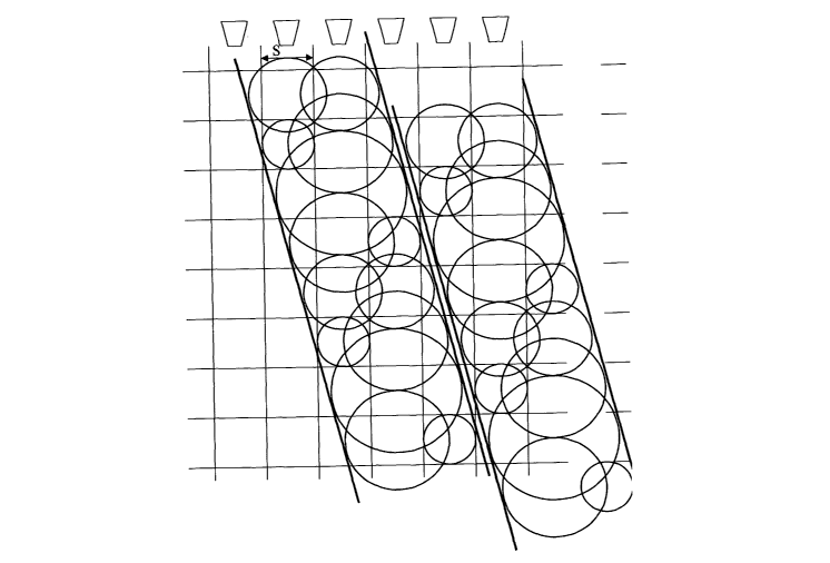
Referring initially to Figure 1, there is shown a conventional ink jet
printing
technique for forming tracks using "binary" printing, that is to say with a
single dot
diameter. Droplets of liquid are deposited from nozzles 10 using any
appropriate
ink jet printing technology. These nozzles 10 are spaced at a distance s and
the
dots formed by the ejected ink droplets lie on a rectangular grid having a
spacing
s in the direction along the nozzle array and a dimension in the orthogonal
direction which is determined by the rate of scanning of the substrate past
the
nozzle array and the frequency of droplet ejection. This dimension may
typically
also be s. It will be understood that dots can be formed at a spacing which is
less
than the nozzle spacing s in the direction of the nozzle array with multiple
passes
of the nozzle array over the substrate.
In this arrangement, each dot is of a uniform size equal to s 2. Each dot
overlaps the edge of adjacent pixel by distance which is equal to (s 2-s). The
intended edges of the tracks in Figure 1 are shown by lines 2. It will be seen
that
at some points (for example those marked at 4 and 6) approximation to the line
2
is poor. However, no greater accuracy is possible in a single pass operation
at a
given value s. Looked at another way, the width of the track varies
considerably
with the track being at some point two dots wide and at other points three
points
wide. For the very narrow tracks increasingly required in the fabrication of
elctronic circuitry, this variation in track width leads to an unacceptable
increase
in resistance and high frequency emissions. It will also be apparent that the
minimum inter-track spacing is equal to (s-2 (s 2-s)),. At most points along
the
tracks, however, the inter-track spacing is significantly greater. This will
not
generally give the required efficiency in circuit board utilisation.
Figure 2 illustrates a prior art attempt to print the same tracks, now with a
number of different dot diameters in "grey scale" printing. In a typical
arrangement the largest dot diameter corresponds to the dot diameter s 2 of
the
binary system illustrated in Figure 1, but a number of smaller dot diameters
are
provided, in this case two such smaller dot diameters. With a printed image,
the
SUBSTITUTE SHEET (RULE 26)
CA 02556298 2006-08-11
WO 2005/081597 PCT/GB2005/000515
-7-
grey scale approach would be expected to produce a significantly straighter
perceived edge. In the present situation, however, it will be seen that the
smallest
dot size when placed along the edge of the track to improve the perceived
straightness, actually has very little effect upon the conductivity of the
track since
each of these smallest dot sizes typically abuts only one of the neighbouring
dots.
An arrangement according to the present invention will now be described
with reference to Figure 3. As with the previous figures, nozzles 10 are
illustrated
schematically at a nozzle spacing s, this spacing defining a grid 32 with
reference
to the substrate. This grid is depicted as square although it will be
understood
that the dimension in the direction orthogonal to the nozzle array (that is to
say
the vertical dimension in the drawing) need not necessarily be equal to s. In
the
arrangement of Figure 3, four dot diameters D are employed. Each dot is
centred
on a grid square, the smallest dot diameter D being set equal to s. The next
size
dot diameter is chosen so that the circumference of the dot overlaps the
adjacent
grid squares by up to one quarter of the width of that grid square. That is to
say,
the next dot diameter is chosen so that D2 = 1.5s. Similarly, the remaining
dots
are chosen so as to overlap by 50% and 75% respectively the adjacent grid
squares, taking values D3 = 2s and D4 = 2.5s. Generalising to a value n of dot
diameters, it will be seen that these dot diameters DI are given by:
D; = 2s(1/2 + i/n), where i is a running integer from 0 to (n-1 )
The dot patterns which are used to form the narrow, closely spaced tracks
are highly ordered. It will be seen that the pattern of dots produced by the
droplets from a single nozzle (that is to say a vertical column in the
representation of Figure 3) form an ascending sequence D~, D2, D3, D4 and a
descending sequence D4, D3, D2, D~. This ascending and descending sequence
from the smallest dot diameter to the largest dot diameter and back to the
smallest dot diameter has particular preferred characteristics in the ability
to form
narrow closely spaced tracks over a range of angles (with respect to the grid
axis).
This explanation concentrates on the minimum track width for the reason
that it is straightforward to produce tracks of larger width. Such larger
track
widths can be formed by repeating the characteristic dot patterns shown in
Figure 3. In certain cases, and typically with larger track areas, it will be
appropriate to use the characteristic dot patterns shown in Figure 3 at the
edges
SUBSTITUTE SHEET (RULE 26)
CA 02556298 2006-08-11
WO 2005/081597 PCT/GB2005/000515
-$_
of the wide track with possibly other dot patterns in the centre of the track
region.
Those other dot patterns may be chosen to optimise efficiency of area
coverage.
The minimum track width achievable with the arrangement of Figure 3 at an
arbitrary angle is:
TW = s(3n-2)/n
At an arbitrary angle, the preferred arrangement guarantees a minimum
spacing of tracks parallel to the grid axis of s/n (with s being replaced by
the
other grid dimension if a non-squared grid is employed).
The grid depicted in the figures is at a spacing of 360dpi i.e. the centre of
each dot is approximately 70pm apart in each axis. This equates to distance s.
The shown grid could, however, be 720, 1440 or 2880dpi or some other
resolution. The dots are deposited by an inkjet print head into the centre of
each
of the addressable pixels.
The arrangement depicted in Figure 4 produces an increased track width.
It will be seen that in this case, the ascending and descending sequences of
dot
diameters D~, D2, D3, D4, still define the track edge, but instead of
inserting an
increased diameter D5 in the sequence, the "central" diameter in the sequence
is
D4 with the increased track width arising from the appearance in the same row
of
the grid of a dot diameter D~ from the "end" of a sequence in the left-hand
neighbouring column and a dot diameter D~ at the "beginning" of a sequence in
the right-hand grid column. This approach can be extended by replacing the dot
at the centre of the ascending and descending sequence by a dot of diameter
D2,
this dot then cooperating with equal size dots in the left-hand and right-hand
neighbouring grid columns to form an incrementally wider track.
Figure 5 illustrates tracks formed at four different angles. In each case
n=4 and the drop diameters are:
Do = 1.Os
D, = 1.5s
D2 = 2.Os
D3 = 2.5s
Figure 5 shows (at A) parallel tracks having a width 2.5s at an angle
arctan 2. It will be seen that the tracks are formed from the repeating drop
SUBSTITUTE SHEET (RULE 26)
CA 02556298 2006-08-11
WO 2005/081597 PCT/GB2005/000515
_g_
pattern D~, D3, D~ with each repeat of the pattern being offset a distance s
horizontally (in the drawing) and a distance 2s (thus giving arctan 2)
vertically.
At (B), an arrangement is shown with the repeating pattern
Do, D~, D3, D~, Do offset a distance s horizontally (in the drawing) and a
distance
3s vertically, providing a track angle of arctan 3. It is important to note
that this
different angle is achieved without a change in track width.
At (C), an arrangement is shown with the repeating pattern
Do, D,, D2, D3, D2, D~, Do offset a distance s horizontally (in the drawing)
and a
distance 4s vertically, providing a track angle of arctan 4. Again, that this
different angle is achieved without a change in track width.
The diagrams (A), (B) and (C) illustrate examples of the pattern:
Do,D~,D2,...D;,...D"_~,...D;,...D2,D~,Do
with dots in the pattern being progressively removed for increasing angles
from
(C) to (A). To decrease the angle from that of (C), dots in the pattern can be
repeated. Thus Figure 5 shows at (D) the repeating pattern Do, Do, D~, D2, D3,
D2, D1, Do, Do to provide an angle of arctan 5.
Figure 6 shows at (A), (B) and (C) tracks of minimum width 2.6s with five
dot sizes:
Do=s
D~ = 1.4s
D2 = 1.8s
D3 = 2.2s
D4 = 2.6s
At (A), tracks are shown formed from the repeating drop pattern D~, D4, D~
with each repeat of the pattern being offset a distance s horizontally 2s
vertically.
At (B), an arrangement is shown with the repeating pattern
Do, D~, D3, D4, D3, D~, Do offset a distance 4s vertically, providing a track
angle
of arctan 4.
At (C), an arrangement is shown with the repeating pattern
Do, D~, D2, D3, D4, D3, D2, D,, Do offset a distance 5s vertically, providing
a track
angle of arctan 5. Again, note that these different angles are achieved
without a
change in track width. Similarly, angles can be increased or decreased by
omitting or repeating drops in the repeating pattern.
A further embodiment of the invention is illustrated at Figure 7. The tracks
may be formed in a single pass of the print head as a single dot is displayed
in
SUBSTITUTE SHEET (RULE 26)
CA 02556298 2006-08-11
WO 2005/081597 PCT/GB2005/000515
-10-
each addressable pixel. One of a number of predetermined dot sizes may be
displayed in a respective pixel. In contrast to the conventional greyscale at
least
one, and preferably two or more of the predetermined dots have a diameter that
is greater than s 2. The dots shown have diameters on the substrate that
increase by a substantially regular amount i.e. s, 1.5s, 2s and 2.5s.
Using the above dot sizes enables the addressability of an edge to within
s/n and therefore the approximation of a desired track edge location to within
s/n.
As can be seen from Figure 7, this ability to address an edge enables the
tracks
to be spaced with a smaller inter-track spacing than with a binary or
conventional
greyscale display that is equal, in the smallest case, to s/n.
Where a track is provided that has two parallel edges it is preferred in this
embodiment that the edges are spaced at least 3s apart. This ensures that both
edges can be approximated by respective dots to similar degrees of accuracy.
The addressability of a row of dots to an edge will be described in greater
detail with respect to Figure 8 to Figure 11. These figures show a corner
printed
first in binary, Figure 8, and secondly with the multiple dot sizes according
to the
present invention. All the figures are displayed at the same pixel grid
addressability.
For the binary (prior art) print of Figure 8a to d, where a single dot size is
displayed, it is clear that an edge 10, 12 may be addressed to a single point
in
the pixel. Thus, for example, if an edge is required to be addressed at a
point
equal to x% across a pixel, as shown by hatchedline 16, the error is equal to -
((x/100.s)-(s-s 2)) or + (s 2-(x/100.s)). Clearly, at certain values of X, for
example 80% the error is quite large either -0.38s or +0.61 s. This places
significant constraints on image quality and the location of the edge.
For a conventional greyscale image, where a plurality of dots smaller than
the size of the grid spacing s is used, and the dots are displayed at the
centre of
the each of the addressable pixels, the maximum error is given by the
equation:
+/-'/2((1/2s + rsd/100.s) - (rld/100.s - s))
where rsd is the radius of the smallest drop and rld is the radius of the
largest
drop as percentages of s.
For the situation where the radius of the largest drop is 1.4s i.e. rld=140%
of s and the radius of the smallest drop is 0.2s i.e. 20% of s, the maximum
error
displayed is equal to +/- 0.15s i.e. 15% of s. This maximum error would be the
SUBSTITUTE SHEET (RULE 26)
CA 02556298 2006-08-11
WO 2005/081597 PCT/GB2005/000515
-11
same regardless of the number of grey levels used between the largest and
smallest drops.
It will be apparent that there is a natural limitation to the minimum drop
volume that may be ejected since as the volume decreases the relative air drag
increases to a point that an unachievable velocity is required from the print
head
to ensure the droplet reaches the substrate. The current limit on the smallest
drop volume would be around 2p1, which would provide a dot size of the order
23
pm on the substrate. This, for a 70 pm grid spacing, equates to just over 30%
of
the grid.
It is important to remember that for a displayed image, where there is no
requirement for dots to touch, it may be acceptable to use the smaller dot
sizes.
Where the dots conduct electricity it will be apparent that the smallest dot
in the
above example will only touch a neighbouring dot in one axis leading to a
higher
resistance in the image, as described with reference to Figure 2.
An aspect of the present invention will now be further described with
reference to Figures 9 to 11. Figure 9a to d depicts an track edge having a
line
10 approximated by dots and a second line 12 similarly approximated by dots.
The first profile 10 is fixed with respect to the pixel grid and the second
profile 12
is varied in accordance with a desired edge addressability. As can be seen,
where each dot has a regular increase in size over a smaller dot and where the
smallest dot has a diameter equal to s, and the largest diameter is equal to
2.6s
then the profile 12 may be addressed to within s/n, where n in this case is 3.
The
maximum error is therefore '/2 s/n.
The addressability of profile 10 may similarly be defined to within a
distance of s/n as depicted self evident manner in Figures 10 and 11.
By adding in further predetermined dot sizes at a regular increase in size
it is possible to further improve the edge addressability. There is
fundamentally
no inherent limitation to the edge addressability that may be achieved.
A further advantage of the present invention lies in the ability to
compensate for drop landing or other dot positioning errors. Figure 12a
depicts
track having an inclined track edge 2. Each dot is perfectly centred on the
grid
and can accurately approximate the smoothed profile 2 using 3 different drop
sizes. In Figure 12b, one of the dots formed by the print head has an error in
the
Y or scanning direction. If the same algorithm is used to produce the image as
SUBSTITUTE SHEET (RULE 26)
CA 02556298 2006-08-11
WO 2005/081597 PCT/GB2005/000515
-12
used to form the image of Figure 12b, then the line 2 does not produce the
best
fit.
In single pass printing, where each column is produced by a single dot
generating element it is possible to modify the algorithm such that the dot
size
produced by the dot generating element is modified either to increase or
reduce
the size of the dot such that the profile is better approximated, as depicted
in
Figure 12c.
The change may be permanent in that it is applied to every future image or may
be varied on an image by image basis.
It is also think of arrangements according to the present invention serving
to shift the "centre of gravity" of a track by modifying the weighting of dots
used to
form the track. Using a print head, commercially available from Xaar under the
trade name "LEOPARD" it is possible to print fifteen different sizes of drop
as
depicted in Figure 13, the typical diameters of the dots are given in the
table
below.
Number of sub-droplets Typical diameter
per dot (dpd) (Nm)
1 39
2 55
3 68
4 78
5 87
6 96
7 103
8 110
9 117
10 124
11 130
12 135
13 141
14 146
15 151
In Figure 14, the dot sizes can be used to generate very slight angles to a
track. These angles can be modified in succession, thereby producing accurate
and smooth curves, which can maximise efficiency of the track and minimise HF
emissions.
SUBSTITUTE SHEET (RULE 26)
CA 02556298 2006-08-11
WO 2005/081597 PCT/GB2005/000515
-13-
Figures 15 to 17 depict actual images printed by an inkjet print head
depositing 4 dot sizes on the substrate. Figure 15 is printed in binary and
the
tracks have a width ranging between 150 microns and 280 microns. By contrast,
Figure 16 is a corresponding track printed via a routine according to the
present
invention. The track has a more uniform width that that of the track printed
in
binary. Figure 17 depicts a plurality of tracks printed side by side. The
upper
tracks have a pitch of 371 Nm, whilst the lower tracks have an inter track
spacing
of 389pm.
In another aspect of this invention, attention can be focused not upon the
tracks themselves but on the gaps between them. In certain applications there
will be the need to establish a minimum gap between two tracks, where the
track
edges are not straight lines. According to this invention, with a set of n dot
diameters D; = 2s(1/2 + i/n), where i is a running integer from 0 to (n-1 );
pairs of
dots are formed at respective sides of the gap at locations spaced by 2s. It
is
then ensured that the sum of the diameters of the pair of dots equals 2s(2n-1
)/n.
This is illustrated in Figure 18, where a track arrangement is formed from a
set
of five dots having dot diameters:
Do=s
D~ = 1.4s
D2 = 1.8s
D3 = 2.2s
D4 = 2.6s
It will be that at either side of each gap, pairs of dots are formed, with
centres spaced by 2s. Only the pairs Do /D4 , D~ /D3 and D2 /D2 are employed.
These pairs are characterized in that their diameters sum to s + D4. This can
be
more generally expressed as 2s(2n-1 )/n.
Figure 14 also illustrates the feature that by forming two gaps of the same
form closely together, a track can be produced of narrow width and arbitrary
form.
It will be understood that this invention has been described by way of
examples only and that a wide variety of developments and modifications are
possible without departing from the scope of the invention.
Thus for larger track areas, it may be preferable to use the above-
described techniques to define the track edges, with alternative dot
structures
used to fill in the bulk of the track. Multi-layer printed circuit boards can
be
SUBSTITUTE SHEET (RULE 26)
CA 02556298 2006-08-11
WO 2005/081597 PCT/GB2005/000515
-14
formed, with the above-described techniques also used to create
interconnecting
vias or insulating patterns.
In a further example, conductive tracks can be formed not only by the
direct printing techniques that have been described in detail, but also by
indirect
techniques. Thus the above described techniques can be employed to form an
etch mask, used subsequently to form conductive tracks.
Whilst the present invention has been described above with respect to
dots printed on a substrate and especially dots printed on a substrate in a
single
pass of an inkjet print head, other methods of generating the dots are
envisaged.
The term "track" is not intended to be limited to an electrically conducting
track.
Other applications in which the present application may also be of benefit are
those in which a surface texture or profile is required from a single pass of
a print
head. Such textures or profiles may be required for artistic purposes or
functional
purposes e.g. creating bumps for solder, wells for containing other material,
pressure pads, separators, or lenses. The invention may also be used in the
generation of optical displays or images projected onto a surface. For optical
displays, the displays may be static or they may display variable image data.
OLEDs or LEDs may display the image.
By forming the same or different arrangements of tracks in repeated
layers, three dimensional structures may be constructed .
SUBSTITUTE SHEET (RULE 26)