Note: Descriptions are shown in the official language in which they were submitted.
CA 02556477 2006-08-16
WO 2005/081853 PCT/US2005/005139
INTEGRATED LENS AND CHIP ASSEMBLY FOR A DIGITAL CAMERA
Inventors: Vidyadhar Sitaram Kale; Samuel W. Tam; and Dongkai Shangguan
BACKGROUND OF THE INVENTION
Field of the Invention
The present invention relates generally to the field of digital camera
devices, and
more particularly to a novel combined array chip and lens apparatus. The
predominant
current application for the inventive integrated lens and chip assembly is in
the production of
low cost cameras, wherein the ability to produce high quality pictures without
expensive or
complicated camera assemblies is an important factor.
Description of the Background Art
Very small digital camera modules, adapted for use in small inexpensive
cameras, cell
phones, hand held devices, and the like, are greatly in demand. In the prior
art, such modules
have included generally conventional integrated chip and/or chip on board
assemblies, which
are enclosed in a mechanical housing. A lens block or assembly is attached to
the chip
housing and mechanically aligned thereto. This arrangement requires a
significant quantity
of parts used in the attachment process. It also generally requires some sort
of attachment
apparatus or 'jig for holding the pieces in alignment while they are attached.
It is also very
labor intensive. Additionally, the attaclnnent mechanism is generally rather
delicate and can
easily be jarred out of position if the resulting device is dropped, or the
like.
It would be desirable to have a method for producing a small camera module
which is
small in size, inexpensive to manufacture, and durable and reliable in
operation. However, to
the inventors' knowledge, the above described arrangement of components is
that being used
in the production of such devices prior to the advent of the presently
described invention.
1
CA 02556477 2006-08-16
WO 2005/081853 PCT/US2005/005139
SUMMARY
Accordingly, it is an object of the present invention to provide a camera
module which
is easy and inexpensive to manufacture.
It is another object of the present invention to provide a camera module which
can be
very small in size.
It is still another object of the present invention to provide a camera
module, which is
rugged and reliable in operation.
It is yet another object of the present invention to provide a camera module
in which
the lens is accurately located, thereby providing for optimal picture quality
without the need
for active alignment.
Briefly, an example of the present invention has a lens assembly, which is
rigidly
affixed in relationship to a camera chip using a molded component. The molded
component
is formed in place on a printed circuit board on which the camera chip is
already mounted.
The lens assembly is then inserted into the molded component and held in place
therein by an
adhesive. According to the present inventive method and apparatus, a lens is
accurately
affixed in relationship to the sensor surface of the camera chip using a
minimum of
components and a minimum of operations steps. The size of the resulting unit
can be quite
small and the unit is also rugged and reliable in operation.
These and other objects and advantages of the present invention will become
clear to
those skilled in the art in view of the description of modes of carrying out
the invention, and
the industrial applicability thereof, as described herein and as illustrated
in the several figures
of the drawing. The objects and/or advantages listed or discussed herein are
not an
exhaustive list of all possible objects or advantages of the invention.
Moreover, it will be
possible to practice the invention even where one or more of the intended
objects and/or
advantages might be absent or not required in the application.
Further, those skilled in the art will recognize that various embodiments of
the present
invention may achieve one or more, but not necessarily all, of the above
described objects
and/or advantages. Accordingly, the listed objects and advantages are not
essential elements
of the present invention, and should not be construed as limitations.
2
CA 02556477 2006-08-16
WO 2005/081853 PCT/US2005/005139
BRIEF DESCRIPTION OF THE DRAWINGS
Fig. 1 is a cross sectional side elevational view of an example of an
integrated camera
and lens assembly according to the present invention;
Fig. 2 is a top plan view of a partially assembled integrated camera and lens
assembly
according to the present invention;
Fig. 3 is a top plan view of another example of a PCB assembly according to
the
present invention;
Fig. 4 is a bottom plan view of a flexible connector according to the present
invention;
Fig. 5 is a top plan view of an assembled flexible PCB apparatus;
Fig. 6 is a top plan view of a substrate strip such as can be used to
implement the
present invention;
Fig. 7 is a top plan view of a molding chase such as can be used to implement
the
present invention;
Fig. 8 is a cross sectional side elevational view of one of the mold inserts
of Fig. 7;
Fig. 9 is a top plan view showing the substrate strip of Fig. 6 with a
protective tape in
place thereon;
Fig. 10 is a cross sectional side elevational view of an alternative example
of the
inventive integrated camera and lens assembly;
Fig. 11 is a flow diagram depicting the inventive method for producing an
integrated
camera and lens assembly;
Fig. 12 is a flow chart summarizing one particular method for performing a
camera
chip mounting step of Fig. 11;
Fig. 13 is a flow chart summarizing one particular method for performing an
overmolding lens mount step of Fig. 11;
Fig. 14 is a flow chart summarizing one particular method for performing a
device
separation step of Fig. 11; and
Fig. 15 is a flow chart summarizing one particular method for performing a
lens
mounting step of Fig. 11.
3
CA 02556477 2006-08-16
WO 2005/081853 PCT/US2005/005139
DETAILED DESCRIPTION OF THE INVENTION
This invention is described in the following description with reference to the
Figures,
in which like reference numbers represent the same or similar elements. While
this invention
is described in terms of modes for achieving this invention's objectives, it
will be appreciated
by those skilled in the art that variations may be accomplished in view of
these teachings
without deviating from the spirit or scope of the present invention. The
embodiments and
variations of the invention described herein, and/or shown in the drawings,
are presented by
way of example only and are not limiting as to the scope of the invention.
Unless otherwise
specifically stated, individual aspects and components of the invention may be
omitted or
modified, or may have substituted therefore known equivalents, or as yet
unknown substitutes
such as may be developed in the future or such as may be found to be
acceptable substitutes
in the future. The invention may also be modified for a variety of
applications while
remaining within the spirit and scope of the claimed invention, since the
range of potential
applications is great, and since it is intended that the present invention be
adaptable to many
such variations.
In the following description, details of some well known and/or commonly
commercially available component parts have not been specifically discussed in
detail, so as
to avoid unnecessary complexity which might obscure disclosure of the true
nature of the
present invention. It should be noted that the diagrammatic representations in
the drawings
accompanying this description are not necessarily drawn in the scale and
proportion which
might be used in the actual practice of the invention. Rather the drawings are
intended only
to demonstrate the relative arrangement of certain aspects of the invention
and to assist in the
understanding of the important inventive aspects.
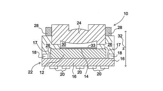
A known mode for carrying out the invention is an integrated camera module.
The
inventive integrated camera module is depicted in a side elevational view in
Fig. 1 and is
designated therein by the general reference character 10. The integrated
camera module 10
has a camera chip 12 which is, in and of itself, not different from other
camera chips such as
are now in use or such as might be developed in the future. One skilled in the
art will
recognize that the camera chip 12 will have thereon a sensor array area 14 and
will also
contain many of the additional components (timing, and the like) necessary or
desirable for
causing the sensor array area 14 to capture an image. In the example of Fig. 1
the camera
chip 12 is attached (as will be discussed in greater detail hereinafter) to a
printed circuit board
4
CA 02556477 2006-08-16
WO 2005/081853 PCT/US2005/005139
("PCB") 16. The camera chip 12 is electrically connected to the PCB 16 by a
plurality (only
two of which are visible in the view of Fig. 1) of wire bond attachment wires
17.
The PCB 16 has thereon a plurality of passive components 18 which, in
conjunction
with components on the camera chip 12, constitute the internal circuitry of
the integrated
camera module 10. Optionally, the PCB 16 can, in some applications, have a
plurality (only
a few of which are shown in the view of Fig. 1 for the sake of clarity) of
bottom contact pads
20 for connecting the integrated camera module 10 electrically to external
components (not
shown), such as an operating button, optional flash circuitry, external
digital memory,
external control circuitry, or the like. Together, the above described
components form a PCB
assembly 22 which, in many respects, is not significantly different from those
currently in use
in similar camera modules.
According to the~present invention, a lens assembly 24 is positioned in
relation to the
PCB assembly 22 by molding 26 and held in place therein by an adhesive 28. The
molding
26 is formed by a molding material on the PCB assembly 22 as will be discussed
in greater
detail hereinafter. The molding 26 has dimensional tolerances sufficiently
accurate such that
when the lens assembly 24 is positioned within a recessed area 29 (Fig. 2) in
the molding 26,
as shown in the example of Fig. 1, then a gap 30 is appropriate for the focus
of the lens
assembly 24 in relation to the PCB assembly 22. Optimal distance between the
lens assembly
24 and the sensor array 14 is determined by the geometry and materials .of the
particular
lenses used. The height of the gap 30 is a function of the placement of the
lens assembly 24
in a Z dimension 32, as can be seen in the view of Fig. l, which placement
will be discussed
in greater detail hereinafter.
Note that lens assembly 24 is not intended to depict any particular lens
design, but
rather is shown representationally for illustrative purposes. Depending on the
particular
design, lens assembly 24 can be formed from a single piece of material, can
include one or
more lenses mounted in a carrier (e.g., Fig. 10), or can inlcude additional
optical components.
A protective cover 33 is mounted over sensor array area 14, to protect sensor
array area
14 from damage during the manufacturing and assembly process. Preferably,
protective
cover 33 is formed from a robust, optically inactive material. In one
particular embodiment,
protective cover is a glass cover sheet, which can be mounted over sensor
array axea 14 either
before or during the formation of molding 26.
Fig. 2 is a diagrammatic top plan view of the integrated camera module 10 of
Fig. 1
before the lens assembly 24 is positioned thereon. As can be seen in the view
of Fig. 2,
5
CA 02556477 2006-08-16
WO 2005/081853 PCT/US2005/005139
placement of the lens assembly 24 (Fig. 1) in an X dimension 36 and a Y
dimension 38 is
accomplished by the position and tolerances of the recessed area 29 in the
molding 26. An
aperture 38 in the molding 26 is provided such that the sensor array area 14
can be seen there
through.
Fig. 3 is a top plan view of another example of a PCB assembly 22a. In the
example of
Fig. 3 it can be seen that the camera chip 12 is affixed (by an adhesive, in
this example) to the
alternate PCB 16a. A great plurality of the attachment wires 17 are connected
to a like
plurality of attachment pads 42 on the alternate PCB 16a for making electrical
connection
between the alternate PCB 16a and the camera chip 12. The alternate PCB
assembly 22a also
has a plurality of attachment forgers 40 thereon for electrically connecting
the alternate PCB
assembly 22a to external circuitry. Unlike the example of Fig. 1, in the
example of Fig. 3, all
of the passive components 18 are located on one side of the camera chip 12.
Fig. 4 is as bottom plan view of a flex circuit 44. The flex circuit 44 has a
plurality of
the attachment forgers 40 thereon for mating with the like plurality of
attachment fingers 40
on the alternate PCB assembly. Furthermore, the flex circuit 44 has a
plurality of edge
connector pads 46 for connection to external circuitry.
Fig. 5 is a top plan view of an assembled flex circuit assembly 48 having the
alternate
PCB assembly 22a of Fig. 3 affixed to the flex circuit 44 of Fig. 4. It should
be noted that the
alternatePCB assembly 22a could be attached directly to a rigid circuit board,
or the like,
without the flex circuit 44. However, in some applications, the flex circuit
44 will allow
more freedom in the placement of the alternate PCB assembly 22a. Furthermore,
additional
circuitry can be included on the flex circuit 44 as may be necessary or
required. The flex
circuit 44 will include traces (not shown) for providing electrical connection
between the
attachment fingers 40 and the edge connector pads 46 and, as discussed above,
optional
additional circuitry as required.
In the view of Fig. 5 it can be seen that, in the flex circuit assembly 48,
the alternate PCB
assembly 22a is connected to the flex circuit 44 at a hot bar attachment point
50 such that the
attachment fingers 40 (not visible in the view of Fig. 5) mate as required.
One skilled in the
art will be familiar with the hot bar attachment method whereby the components
are joined at
the hot bar attaclnnent point 50.
Fig. 6 is a top plan diagrammatic view of a substrate strip 52. The substrate
strip 52 has
a plurality (100 in 'the example shown) of the individual PCBs 16a included
therein. The
substrate strip 54 also has a plurality (18 in this example) of alignment
holes 54 for aligning
6
CA 02556477 2006-08-16
WO 2005/081853 PCT/US2005/005139
the substrate strip 52 in one or more placement jigs (not shown).
Fig. 7 is a top plan diagrammatic view of a mold chase 56 such as might be
used to
accomplish the present invention. The mold chase 56 is constructed of a metal
such as
stainless steel. The mold chase as adapted for holding in place a plurality
(100 in this
example) of mold inserts 58. The mold inserts 58 axe positioned such that one
mold insert 58
is correctly aligned over each of the PCBs 16a on the substrate strip 52 (Fig.
6) when the
mold chase 56 is aligned over the substrate strip 52.
Fig. 8 is a diagrammatic side elevational view of one of the mold inserts 58
in position
over one of the alternate PCB assemblies 22a. As will be discussed in greater
detail
hereinafter, the alternate PCB assemblies 22a are constructed on the substrate
strip 52, except
as noted herein, before the substrate strip 52 is separated into the
individual alternate PCB
assemblies 22a. As can be seen in the view of Fig. 8, mold insert 58 is coated
with a
compliant, nonadherent layer of material 59, to prevent damage to the
underlying sensor 12
and/or to prevent adhesion of the molding 26 material to mold insert 58. The
specific
material used for coating 59 will depend on the specific composition of
molding 26, as is
known to those skilled in the art, and in some applications, coating material
59 can be
omitted. Thus, coating material 59 is not considered to be an essential
element of the present
invention. It should be noted that the molding process, itself, is not
peculiar to the present
invention. In place molding techniques are well known in the art, and one
skilled in the art
will be familiar with the details necessary to properly form the molding 26
and equivalents
discussed herein.
Fig. 9 is a top plan view of an example of the substrate strip 52 with a
protective tape
60 in place thereon to protect the PCB assemblies 16a (not visible in the view
of. Fig. 9)
during some assembly of the invention. Use of the protective tape 60 will be
discussed in
greater detail hereinafter in relation to the inventive method for producing
the integrated
camera module 10.
Fig. 10 is yet another example of an integrated camera module l0a according to
the
present invention. In the view of Fig. 10 it can be seen that an alternate
lens assembly 24a
has a plastic lens housing 62, a first lens 64 and a second lens 66. One
skilled in the art will
recognize that the integrated camera module l0a will generally require two
lenses.
Therefore, an arrangement such as is illustrated in the view of Fig. 10 is
considered by the
inventors to be optimal. However, the invention can be practiced using only
one lens. The
distance between the first lens 64 and the second lens 66 is fixed by the
construction of the
7
CA 02556477 2006-08-16
WO 2005/081853 PCT/US2005/005139
lens housing 62. The distance between the first lens 64 and the camera chip 12
is set as will
be discussed hereinafter. In the example of Fig. 10, an adhesive well 70 is
provided around
the circumference of the molding 26 for accepting the adhesive 28 which holds
the lens
assembly 24a in place within the molding 26.
Fig. 11 is a flow diagram depicting an example of the present inventive camera
module construction method 100. In this particular example, a plurality of
camera modules
are constructed at the same time. First, in a "camera chip mounting" operation
102, one or
more camera chips 12 are mounted to one or more PCBs 16a, respectively (Fig.
6). Next, in a
"lens mount overmolding" operation 103, a lens mount 26 is molded over each
camera chip
12. Then, in a "device separation" operation, the PCBs 16a are separated
(e.g., sawn apart)
from one another. Next, in a "lens mounting" operation 105, a lens housing 62
is mounted
into each lens mount molding 26 (Fig. 10). Finally, in a "packaging" operation
106, the
completed integrated camera modules l0a are packaged for shipment to the
makers of
miniature cameras, telephone cameras, and the like, or optionally for
attachment to the flex
circuit 44 as previously discussed herein.
Fig. 12 is a flow chart summarizing one particular method 107 for performing
camera
chip mounting operation 102 of method 100. First, in a "protective cover
position" operation,
protective cover 33 is positioned over camera chip 12 (Fig. 10). Optionally,
protective cover
33 can be positioned during lens mount overmolding operation 103, at another
point in
camera chip mounting operation 102, or omitted. Next, in a "solder paste
print" operation
110 solder paste traces are printed on the individual PCBs 16a of the
substrate strip 52. In a
"passive attach" operation 112 the passive components 18 are placed on the
PCBs 16a. In a
"reflow" operation 114, the substrate strip 52 is subjected to a reflow
soldering operation, and
in a "cleaner" operation 116, the substrate strip 52 is subjected to
conventional cleaning
following the reflow soldering process 114.
In a "die bonding" operation 118 the camera chips 12 are bonded (by an
adhesive in
this example) to the respective PCBs 16a. In an "oven curing" operation 120,
the adhesive
applied in the previous operation is cured in an oven. In a "plasma cleaning"
operation 122
surfaces to which wires are to be bonded (in subsequent operations) are etched
using inert
gasses. In a "wire bonding" operation 124 the attachment wires 17 are bonded
using
thermosonic bonding. In a second "plasma cleaning" operation 126 the PCBs 16a
are again
cleaned.
8
CA 02556477 2006-08-16
WO 2005/081853 PCT/US2005/005139
Fig. 13 is a flow chart summarizing one particular method 127 of performing
lens
mount overmolding operation 103 of method 100. In a protective cover
positioning operation
128, protective cover 33 is positioned over camera chip 12. Note that this
step is unnecessary
if protective cover 33 has already been mounted as part of a prior process, or
if no protective
cover is desired. Then, in an "over molding" operation 129, the mold chase 56
is placed over
the substrate strip 52 and the molding 16 is formed as previously discussed
herein. In
addition to the functionality already described herein, molding 16 can also
serve to hold
protective covering 33 in place, essentially sealing in the sensor array area
14 of camera chip
12. The molding 26 is formed using generally conventional "overmolding"
techniques
known to those skilled in the art. The mold will provide for exposure of the
sensor array area
14 of the camera chip 12 after the molding operation. Finally, in an "O/M
curing" operation
130, the molding 26 is briefly heat cured.
Fig. 14 is a flow chart summarizing one particular method 131 of performing
device
separation operation 104 of Fig. 11. First, the protective tape 60 is placed
over all of the
PCBs 16a (as illustrated in Fig. 9) in an "attach cover tape" operation 132.
Then, in a "saw
singulation" operation 134, the individual PCBs 16a are sawn apart. The sawing
is done right
through the protective tape 60 such that the resulting product is a plurality
of the individual
PCB assemblies 22a, each having a respective portion of the protective tape 60
still in place
thereon. The protective tape 60 is a commonly available commodity provided for
protecting
components during a soldering process, and the like. Finally, in a "remove
cover tape"
operation 138, the bits of the protective tape 60 are removed from each of the
PCB
assemblies 22a.
Fig. 15 is a flow chart summarizing one particular method 139 of performing
lens
mounting operation 105 of method 100. In a "lens mounting" operation 140, one
of the lens
assemblies 24a is inserted into each of the moldings 26 (Fig. 10). In a "focus
and testing"
operation 142, the lens assembly 24a is moved up and down (along the Z axis 32
of Fig. 1) to
perfect the focus of the lens assembly 24a in relation to the sensor array
area 14 of the camera
chip 12. Correct focus is determined by generally conventional automatic
testing equipment.
It should be noted that the inventors believe that this operation might be
eliminated in the
future by referencing the position of the mold chase 56 in relation to the
camera chip 12
during the "over molding" operation 128. Finally, in a "glue dispensing and
curing"
operation 144, ultra violet cure adhesive 28 is applied as previously
discussed herein, and
then cured using ultra violet light.
9
CA 02556477 2006-08-16
WO 2005/081853 PCT/US2005/005139
Various modifications may be made to the invention without altering its value
or scope.
For example, the sizes, shapes and quantities of components shown and
described in relation
to the examples discussed herein could each or all be varied according the
needs or
convenience of a particular application.
Similarly other substrate materials, such as ceramics, could be used instead
of the PCB
16 described herein.
Another modification would be to replace the air filled gap 30 described
herein with
an optically clear spacer made, for example, of clear plastic, glass, or some
other optically
acceptable material. Providing a spacer which abuts both the camera chip 12
and the lens 24
could eliminate the need to focus the lens during the lens mounting operation.
Also,
secondary lenses, such as zoom lens assemblies and the like, can be fit to the
already
mechanically centered lens assembly 24 or 24a. A spacer would also serve as a
protective
cover, thereby eliminating the need to provide a separate protective cover.
While the inventors presently believe that mounting the lens assemblies 22,
22a into
the molding 26, or the like, by an adhesive is presently the most viable
method, it is within
the scope of the invention that the lens assemblies 22, 22a could be secured
to the PCB 16,
16a in relation to the camera chip 12 by other mechanical means, such as a
mechanical clip,
or the like.
Obvious variations to the method could include mounting the lens assemblies
24a into
the molding 26 before the "saw singulation" operation 134. Of course, this
would require
some other modifications to the method to insure that the sensor array area 14
is protected
during the "saw singulation" operation 134, and the like.
Additional components and/or parts could readily be added to the present
invention.
One possible example would be to provide a glass cover on the molding 26. Such
as cover
might serve several purposes. It could protect the sensor array area 14 during
storage,
transport and handling, it could optionally provide a service whereby the
device could be
lifted by "pick-and-place" machines, and it could protect the sensor array
area 14 during
reflow soldering operations.
All of the above are only some of the examples of available embodiments of the
present
invention. Those skilled in the art will readily observe that numerous other
modifications and
alterations may be made without departing from the spirit and scope of the
invention.
Accordingly, the disclosure herein is not intended as limiting and the
appended claims are to
be interpreted as encompassing the entire scope of the invention.
CA 02556477 2006-08-16
WO 2005/081853 PCT/US2005/005139
INDUSTRIAL APPLICABILITY
The inventive integrated camera module 10, l0a is intended to be widely used
for
capturing visual images in very small devices such as small digital cameras,
cellular
telephones, and the like. The device and method are appropriate to a wide
variety of
applications, including using sensor modules ranging from VGA resolution to
1.3 Megapixel
or even greater. The method and apparatus described herein are inexpensive in
the molding
material and process is lower in cost as compared to the attachment of a
housing using
conventional methods. This is mainly because the molding process will be
performed on an
entire panel having thereon a large number of the integrated camera modules 10
at once,
rather than attaching the lenses one at a time. Also, the cost of molding
compound will be
lower than the cost of individual housing pieces formerly used for attaching
the lenses.
According to the present invention, the final assembly of the integrated
camera
modules 10 will be more robust and more accurate with respect to X and Y
locations. This is
accomplished by ensuring that the sensor die placement and the overmold insert
locations are
controlled by the same local fiducial features on the substrate. Current
methods involve use
of guide pins and other means for the placement of the housing. These
inherently involve
greater tolerance build up compared to a mold with greater dimensional
accuracy and more
stable dimensions.
As discussed previously herein, Z dimension accuracy will be accomplished with
reference to the camera chip 12 surface itself, which is the key reference for
camera focus. It
is anticipated that, in the future, this will obviate the need for active
alignment in most cases.
Also, the fact that the alignment is done without having to rotate the lens
assembly into a
threaded housing will inherently make the lens placement more stable.
It is further anticipated that the reduction in the required number of
components
according to the present invention will, itself, result in additional cost
savings.
Since the integrated camera module 10, l0a of the present invention may be
readily
produced and integrated with existing design configurations for camera systems
and others
yet to be conceived, and since the advantages as described herein are
provided, it is expected
that it will be readily accepted in the industry. For these and other reasons,
it is expected that
the utility and industrial applicability of the invention will be both
significant in scope and
long-lasting in duration.
11