Note: Descriptions are shown in the official language in which they were submitted.
CA 02556754 2006-08-17
WO 2005/082236 PCT/US2005/005913
MULTI-BIT ADC WITH SIGMA-DELTA MODULATION
BACKGROUND OF THE INVENTION
[0001] The present invention relates to oximeters, and in particular to sigma-
delta
modulators used in connection with analog-to-digital conversion in pulse
oximeters.
[0002] Pulse oximetry is typically used to measure various blood chemistry
characteristics
including, but not limited to, the blood-oxygen saturation of hemoglobin in
arterial blood, the
volume of individual blood pulsations supplying the tissue, and the rate of
blood pulsations
corresponding to each heartbeat of a patient. Measurement of these
characteristics has been
accomplished by use of a non-invasive sensor which scatters light through a
portion of the
patient's tissue where blood perfuses the tissue, and photoelectrically senses
the absorption of
light at various wavelengths in such tissue. The amount of light absorbed is
then used to
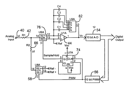
calculate the amount of blood constituent being measured.
[0003] The light scattered through the tissue is selected to be of one or more
wavelengths
that are absorbed by the blood in an amount representative of the amount of
the blood
constituent present in the blood. The amount of transmitted light scattered
through the tissue
will vary in accordance with the changing amount of blood constituent in the
tissue and the
related light absorption. For measuring blood oxygen level, such sensors have
typically been
provided with a light source that is adapted to generate light of at least two
different
wavelengths, and with photodetectors sensitive to both of those wavelengths,
in accordance
with known techniques for measuring blood oxygen saturation.
[0004] Known non-invasive sensors include devices that are secured to a
portion of the
body, such as a finger, an ear or the scalp. In animals and humans, the tissue
of these body
portions is perfused with blood and the tissue surface is readily accessible
to the sensor.
[0005] Typically, the analog-to-digital conversion in a pulse oximeter is done
using a
sigma-delta modulator for analog-to-digital conversion after the signal is
demodulated into
the separate red and lR signals. An example of a pulse oximeter circuit using
sigma-delta
modulators is set forth in U.S. Patent No. 5,921,921. This patent shows the
use of two sigma-
delta modulators, one for the red channel and one for the IR (infrared)
channel. The sigma-
delta modulators provide 1-bit of digital resolution, with the output of the
sigma-delta
modulator being filtered to produce a higher resolution signal. This is
accomplished by using
WO 2005/082236 CA 02556754 2006-08-17 PCT/US2005/005913
a fast oversampling rate (typically 1200 Hz) and then filtering to produce the
slow, high
resolution signal. The gain of the sigma-delta modulator in this patent is
controlled by
varying the width of the feedback pulse.
BRIEF SUMMARY OF THE INVENTION
[0006] The present invention moves the demodulator into the software domain,
after the
Analog-to-digital Converter (ADC). A sigma-delta modulator is used with a
simple ADC.
This allows the use of a single signal path for the photo current signal,
rather than
demodulating into red and IR components as in the prior art, which required
two ADCs. The
red and IR signals are separated later, in the digital domain using a software
or firmware
program. By using the same hardware for both red and IR, there is no gain
error introduced
into one signal but not the other. Since the red and IR will have the same
frequency response
error, the calculation of blood oxygenation will cancel out this error. The
demodulation in
software also allows a more sophisticated demodulation scheme to be used.
[0007] The present invention is able to produce an accurate multi-bit ADC
conversion with
the sigma-delta modulator, rather than the single bit conversion of the prior
art, by using a
multi-bit feedback Digital-to-analog Converter (DAC) to provide a unique Pulse
Width
Modulated (PWM) feedback. The feedback DAC is clocked by a stable clock to
provide a
control output which controls a switch between two voltage references, which
are added back
into the input signal. The amount of time the high voltage reference is added
in versus the
amount the low voltage reference is added in provides a PWM signal to give an
accurate
analog feedback. The invention reduces linearity errors since the feedback is
a function of a
stable clock signal.
[0008] In another aspect of the invention, a switch at the input of the
integrator used for the
sigma-delta modulator provides a sample and hold circuit. An analog switch is
used to
switch between the non-inverting and inverting inputs of the operational
amplifier of the
integrator. The connection to the other input of the operational amplifier
maintains the
voltage of the input to the switch at the same voltage level. A voltage
reference is connected
to this second input (e.g., the non-inverting input) to provide a source or
sink for excess
current, as needed.
[0009] In another aspect of the present invention, multiple capacitors are
used for the
integrator of the sigma-delta modulator. Different capacitors are switched in
depending upon
2
CA 02556754 2012-08-02
the input signal received. This allows a single sigma-delta modulator and ADC
since a
different capacitor can be dedicated to each signal to be demodulated. For
example, a first
capacitor can be used for a red signal and a second for the infrared signal.
Additionally, third
and fourth capacitors can be used for a first dark signal in between the red
and infrared, or a
second dark signal between the infrared and red. Thus, each capacitor stores
the quantization
error for a particular time slot, which allows the sigma-delta modulator ADC
to operate on the
signal before demodulation.
10009a1 Accordingly, there is provided an oximeter apparatus comprising: a
sigma-delta
modulator having an input coupled to receive an analog sensor signal and
further comprising
first and second integrators; a first switching circuit, coupled to said
input, for switching
between connecting first and second reference voltages to said input;
characterized in that the
oximeter apparatus further comprises: a multiple bit analog-to-digital
converter coupled to an
output of said sigma-delta modulator to provide a digital output; and a
feedback circuit
coupled to said output of said sigma-delta modulator, said feedback circuit
including a digital-
to-analog converter having an input coupled to said digital output of said
multiple bit analog-
to-digital converter, and an output coupled to said first switching circuit
for producing a pulse
width modulated output signal controlling the switching between said first and
second
reference voltages by said first switching circuit; and a second switching
circuit, coupled to an
input of said second integrator and controlled by said feedback circuit, for
switching to said
second voltage reference when said first switching circuit connects to said
first voltage
reference, and switching to said first voltage reference when said first
switching circuit
switches to said second voltage reference.
[0009b] There is also provided a circuit comprising: a multi-bit sigma-delta
modulator
having an input adapted to receive a first analog signal representative of
received red light and
a second analog signal representative of received infrared light through a
single path, the
multi-bit sigma-delta modulator being configured to produce a digital output
signal wherein
the multi-bit sigma-delta modulator comprises first and second integrators; a
first switching
circuit, coupled to the input, the first switching circuit being adapted to
switch between
connecting first and second reference voltages to the input; a feedback
circuit, coupled to an
3
CA 02556754 2012-08-02
output of the multi-bit sigma-delta modulator to receive the digital output
signal, the feedback
circuit being adapted to control the switching between the first and second
reference voltages
by the first switching circuit; and a second switching circuit coupled to an
input of the second
integrator and controlled by the feedback circuit, the second switching
circuit being adapted
to switch to the second voltage reference when the first switching circuit
connects to the first
voltage reference, and to switch to the first voltage reference when the first
switching circuit
switches to the second voltage reference.
10009c1 There is also provided a circuit comprising: a multi-bit sigma-delta
modulator
having an input adapted to receive a first analog signal representative of
received red light and
a second analog signal representative of received infrared light through a
single path, the
multi-bit sigma-delta modulator being configured to produce a digital output
signal; wherein
the multi-bit sigma-delta modulator includes an operational amplifier
configured as an
integrator; a first switching circuit, coupled to the input, the first
switching circuit being
adapted to switch between connecting first and second reference voltages to
the input; a
feedback circuit, coupled to an output of the multi-bit sigma-delta modulator
to receive the
digital output signal, the feedback circuit being adapted to control the
switching between the
first and second reference voltages by the first switching circuit; a second
switching circuit
configured to function as a sample and hold by alternately coupling the input
to inverting and
non-inverting inputs of the operational amplifier; and a control circuit,
coupled to the
feedback circuit, the control circuit being adapted to control the switching
of the second
switching circuit.
[0009d] There is also provided a circuit comprising: a multi-bit sigma-delta
modulator
having an input adapted to receive a first analog signal representative of
received red light and
a second analog signal representative of received infrared light through a
single path, the
multi-bit sigma-delta modulator being configured to produce a digital output
signal, wherein
the multi-bit sigma-delta modulator includes an integrator; at least first and
second capacitors;
a capacitor switching circuit adapted to connect the first capacitor to the
integrator upon
receipt of a first sensor signal, and to connect the second capacitor to the
integrator upon
receipt of a second sensor signal, wherein the first sensor signal is
representative of received
3a
CA 02556754 2012-08-02
red light and the second sensor signal is representative of received infrared
light; a first
switching circuit, coupled to the input, the first switching circuit being
adapted to switch
between connecting first and second reference voltages to the input; and a
feedback circuit,
coupled to an output of the multi-bit sigma-delta modulator to receive the
digital output
signal, the feedback circuit being adapted to control the switching between
the first and
second reference voltages by the first switching circuit; and a third
capacitor adapted to
connect to the integrator upon receipt of a dark signal between the red and
infrared signals.
[0009e] There is also provided a circuit comprising: a multi-bit sigma-delta
modulator
having an input adapted to receive a first analog signal representative of
received red light and
a second analog signal representative of received infrared light through a
single path, the
multi-bit sigma-delta modulator being configured to produce a digital output
signal; a
multiple bit analog-to-digital converter coupled to the output of the multi-
bit sigma-delta
modulator to provide the digital output signal; a first switching circuit,
coupled to the input,
the first switching circuit being adapted to switch between connecting first
and second
reference voltages to the input; and a resistor coupled between the first
switching circuit and
the input of the multi-bit sigma-delta modulator; and a feedback circuit,
coupled to an output
of the multi-bit sigma-delta modulator to receive the digital output signal,
the feedback circuit
being adapted to control the switching between the first and second reference
voltages by the
first switching circuit, wherein the feedback circuit, is coupled to an output
of the multiple bit
analog-to-digital converter, the feedback circuit being adapted to control the
switching
between the first and second reference voltages by the first switching
circuit, wherein the
feedback circuit provides a pulse width modulated signal to the first
switching circuit.
[0009f] There is also provided a circuit comprising: a multi-bit sigma-delta
modulator
having an input adapted to receive a first analog signal representative of
received red light and
a second analog signal representative of received infrared light through a
single path, the
multi-bit sigma-delta modulator being configured to produce a digital output
signal, wherein
the multi-bit sigma-delta modulator includes an operational amplifier
configured as an
integrator; a first switching circuit, coupled to the input, the first
switching circuit being
adapted to switch between connecting first and second reference voltages to
the input,
3b
CA 02556754 2012-08-02
wherein the first switching circuit is configured to function as a sample and
hold by
alternately coupling the input to inverting and non-inverting inputs of the
operational
amplifier; a feedback circuit, coupled to an output of the multi-bit sigma-
delta modulator to
receive the digital output signal, the feedback circuit being adapted to
control the switching
between the first and second reference voltages by the first switching
circuit; and a control
circuit, coupled to the feedback circuit, the control circuit being adapted to
control the
switching of the first switching circuit.
10009g] There is also provided a circuit comprising: a multi-bit sigma-delta
modulator
having an input adapted to receive a first analog sensor signal, and a second
analog sensor
signal through a single path, the multi-bit sigma-delta modulator being
configured to produce
a digital output signal, wherein the first analog sensor signal is
representative of received red
light, and the second analog sensor signal is representative of received
infrared light; at least
first and second capacitors; a third capacitor adapted to connect to the
integrator upon receipt
of a dark signal between the red and infrared signals; and a capacitor
switching circuit adapted
to connect the first capacitor to the integrator upon receipt of the first
analog sensor signal,
and to connect the second capacitor to the integrator upon receipt of the
second analog sensor
signal.
[0009h] There is also provided a pulse oximeter circuit comprising: a multi-
bit sigma-delta
modulator having an input adapted to receive a first analog signal
representative of received
red light and a second analog signal representative of received infrared light
through a single
path, the multi-bit sigma-delta modulator being configured to produce a
digital output signal;
and a feedback circuit configured to receive the digital output signal of the
multi-bit sigma-
delta modulator and generate a pulse width modulated signal (PWM), the PWM
signal being
directed to a first switching circuit and a D flip-flop, the first switching
circuit providing a
first or second reference voltage as a feedback signal to the multi-bit sigma-
delta modulator,
the D flip-flop generating a sample and hold signal, the sample and hold
signal controlling a
second switching circuit coupled to the input of the multi-bit sigma-delta
modulator, the
second switching circuit being configured to direct the first and second
analog signals to an
inverting input of the multi-bit sigma-delta during a sampling period.
3c
CA 02556754 2012-08-02
[00091] There is also provided an oximetry device comprising: a multi-bit
sigma-delta
modulator having an input adapted to receive a first analog signal from a
sensor and a second
analog signal from a sensor through a single path, the multi-bit sigma-delta
modulator being
configured to produce a digital output signal representative of the first and
second analog
signals; at least first and second capacitors coupled in parallel to the input
of the multi-bit
sigma-delta modulator; a capacitor switching circuit configured to couple to
the first capacitor
upon receipt of the first analog signal and to couple to the second capacitor
upon receipt of the
second analog signal, wherein the first and second capacitors are selected to
correspond with a
quantization error for the corresponding analog signals; and a feedback
circuit coupled about
the multi-bit sigma-delta modulator, the feedback circuit comprising a sample
and hold circuit
configured to enable the input of the multi-bit sigma-delta modulator during
receipt of the
first or second analog signals and to disable the input during a holding
period.
1000911 There is also provided a method for analog-to-digital conversion
comprising:
converting a digital output signal of a multi-bit sigma-delta modulator to an
analog pulse
width modulated (PWM) signal, the PWM signal having one fixed edge occurring
at a
constant rate and one variable edge; controlling a feedback circuit using the
PWM signal to
provide a first or second reference voltage as a feedback signal; generating a
sample/hold
signal by dividing the PWM signal, the sample/hold signal controlling an input
switch of the
multi-bit sigma-delta modulator; combining the feedback signal through a
resistor with first
and second analog signals to generate a combined signal, the first and second
analog signals
representing a detected red signal and a detected infrared signal; and
alternately coupling the
combined signal to an inverting input or a non-inverting input of an
operational amplifier of
the multi-bit sigma-delta modulator to provide sampling periods or holding
periods,
respectively.
[0010] For a further understanding of the nature and advantages of the present
invention,
reference should be made to the following description taken in conjunction
with the
accompanying drawings.
3d
CA 02556754 2012-08-02
BRIEF DESCRIPTION OF THE DRAWINGS
[0011] Figure 1 is a block diagram of an oximeter incorporating the present
invention.
[0012] Figure 2 is a circuit diagram of a two-stage sigma-delta modulator
according to an
embodiment of the invention.
[0013] Figure 3 is a diagram of a typical sigma-delta modulator output.
[0014] Figure 4 is a circuit diagram of a sigma-delta modulator according to
an embodiment
of the present invention using the sigma-delta modulator for a sample and hold
circuit with an
analog switch to avoid charge injection.
[0015] Figure 5 is a timing diagram illustrating various signals of the
circuit of Figure 4.
[0016] Figure 6 is a circuit diagram of an embodiment of a sigma-delta
modulator
according to the present invention utilizing multiple capacitors in the
integrator.
[0017] Figure 7 is a timing diagram illustrating different signals of the
circuit of Figure 6.
DETAILED DESCRIPTION OF THE INVENTION
Overall System
[0018] Fig. 1 illustrates an embodiment of an oximetry system incorporating
the present
invention. A sensor 10 includes red and infrared LEDs and a photodetector.
These are
connected by a cable 12 to a board 14. LED drive current is provided by an LED
drive
interface 16. The received photocurrent from the sensor is provided to an I-V
interface 18.
3e
CA 02556754 2006-08-17
WO 2005/082236 PCT/US2005/005913
The IR and red voltages are then provided to a sigma-delta interface 20
incorporating the
present invention. The output of sigma-delta interface 20 is provided to a
microcontroller 22
which includes a 10 bit AID converter. Microcontroller 22 includes flash
memory for a
program, and RAM memory for data. The oximeter also includes a microprocessor
chip 24
connected to a flash memory 26. Finally, a clock 28 is used and an interface
30 to a digital
calibration in the sensor 10 is provided. A separate host 32 receives the
processed
information, as well as receiving an analog signal on a line 34 for providing
an analog
display.
[0019] By using a sigma-delta modulator with the unique PWM feedback of the
present
invention, the simple, internal ADC of microcontroller 22 can be used and
still provide the
desired multi-bit precision. The ADC in this embodiment is a 10 bit successive
approximation ADC. The precisely controlled PWM feedback connects in a voltage
reference through switches 58 and 60, which are then summed in summing nodes
with the
input signal at the inputs of the integrators. The averaged summed value,
between the
positive and negative reference voltages, provide the desired feedback. Any
error is fed back
in the following pulse period.
Sigma-delta Modulator
[0020] Fig. 2 is a circuit diagram of a sigma-delta modulator according to an
embodiment
of the present invention, including portions of sigma-delta interface 20 and
microcontroller
22 of Fig. 1. In particular, an analog input on a line 40 is provided through
a resistor 42 to an
inverting input of an operational amplifier 44 configured as an integrator 51
with a feedback
capacitor 46. The non-inverting input is connected to a reference voltage
(Ref). This is
followed, through a connecting resistor 48, by a second operational amplifier
50, connected
as an integrator 53 with a feedback capacitor 52. The output of operational
amplifier 50 is
connected to an analog-to-digital converter 54, which is the 10-bit A/D
converter in
microcontroller 22 of Fig. 1. =
[0021] The digital output is fed back through a "digital-to-analog converter"
56 as a
feedback circuit through a first switching circuit 58 and a second switching
circuit 60. DAC
56 is internal to microcontroller 22, and produces the PWM output signal shown
in Fig. 5. In
response to the PWM control signal, switching circuit 58 alternately connects
a positive or
negative reference on lines 62 and 64 through a resistor 66 to connect with
the input signal to
the inverting input of operational amplifier 44. Similarly, second switching
circuit 60
4
WO 2005/082236 CA 02556754 2006-08-17 PCT/US2005/005913
connects a negative and positive reference, inverted from the connections
shown for
switching circuit 58. These are reference voltages 68 and 70, which are
connected through a
resistor 72 to the inverting input of operational amplifier 50.
[0022] The feedback signal from digital-to-analog converter 56 is a pulse
width modulated
(PWM) signal, such as the typical signal shown in Fig. 3 for a sigma-delta
modulator
illustrating a sine waveform. By using a PWM signal and switching between only
two
voltages, the linearity of the feedback is a function of the clock signal.
Since the clock signal
is stable, and can be divided more accurately than the analog voltage,
linearity errors are
minimized. The multi-bit analog-to-digital converter, rather than the single
bit converter of
prior art devices, allows a more accurate result with a lower sample rate.
This eases the
requirements for decimation filtering in software.
Sample and Hold
[0023] Fig. 4 is a circuit diagram of an embodiment of the invention
illustrating the switch
controlling the input to the integrator in the sigma-delta modulator, with the
switch being
used for a sample and hold circuit. Fig. 4 shows many of the same circuit
blocks as Fig. 2,
such as analog-to-digital converter 54, feedback digital-to-analog converter
56, switching
circuit 58, input resistors 42 and 66, and operational amplifier 44 configured
as an integrator
with capacitor 46. Only a single stage is shown for simplicity, and it is
understood that an
additional integrator 53 as in Fig. 2 could be added as well, with a similar
switch for a sample
and hold for the second integrator.
[0024] Fig. 4 adds a D flip-flop 74 and switching circuit 76. Switch 76
disconnects the
input 40 from the input of operational amplifier 44 for a hold operation. When
the input is
reconnected after the sample has been held, a problem can arise since the
voltage at the input
can vary dramatically due to the feedback circuit through switch 58 and
resistor 66. Since
this feedback switches between a positive and negative voltage, a significant
variation in the
input voltage could occur. For example, the feedback might vary between
approximately 0-3
volts, with the input being around 1 volt. This would result in a 1.5 volt
swing. Such a swing
would cause, upon reconnection to the inverting input of operational amplifier
44, a charge
injection into capacitor 46, which is undesirable.
[0025] The present invention avoids such a charge injection by connecting the
node 73 to
the non-inverting input of operational amplifier 44. This non-inverting input
further is
connected to a reference voltage. This gives the current which would build up
a place to go.
5
CA 02556754 2006-08-17
WO 2005/082236 PCT/US2005/005913
The difference in voltage will result in current flow either toward or away
from the reference
voltage 75. Thus, upon reconnection, there will be minimal charge injection.
The result of
this structure is that the charge injection from the switch will be
essentially constant, to the
extent there is any, and it can be canceled out later by processing in a
digital domain using a
software or firmware program.
[0026] Fig. 5 illustrates certain of the waveforms of the circuit of Fig. 4.
The pulse width
modified (PWM) signal on line 76 at the output of digital-to-analog converter
56 is shown
first. The arrows signify that the width of the pulse will vary depending upon
the signal.
Next, the sample/hold signal on line 78 is shown, the non-inverting output of
D flip-flop 74.
Finally, the voltage out (Vo) signal on line 80 at the output of the
integrator of operational
amplifier 44 and capacitor 46 is shown. As can be seen, the Vo signal decays
while the
PWM signal is high, and increases or integrates while the PWM signal is low as
long as the
sample/hold signal is high. While the sample/hold signal is low, the Vo signal
is held
constant so that it can be sampled. Although illustrated at the same level
each time in Fig. 5,
the levels would vary with the amount of integration and the width of the
pulse from the
PWM feedback signal.
Multiple Capacitor Sigma-delta Modulator
[0027] Fig. 6 illustrates a modification of the circuit of Fig. 4 in which
capacitor 46 of Fig.
4 is replaced by one of four capacitors, Cl, C2, C3, and C4, which are
selected by a
switching circuit 82.
[0028] In a typical prior pulse oximeter, two separate integrators would need
to be used
= with two separate signal paths and demodulation in the analog domain, so
that the two
different integrators could use two different capacitors for the red and IR
signals. By instead
switching in and out capacitors, a single integrator can be used, and the
analog domain
demodulation circuitry can be eliminated. Instead, the red and IR. signals are
time-
multiplexed through the same integrator, with different capacitors being
switched in for the
red and IR signals. In addition, two additional capacitors can be added for
the dark period in
between the red and IR signals. Since the dark signal can vary depending upon
whether it
follows the IR signal, or follows the red signal, two different capacitors can
be provided to
correspond to dark 1 and dark 2 signals. Thus, the present invention allows
the demodulation
of the signal to be moved into the digital domain and be done by a program in
software or
firmware, rather than having it done with hardware. This allows the hardware
circuitry to be
6
CA 02556754 2012-08-02
reduced in size by using only a single signal path, saving not only space and
cost but also
power.
[0029] Fig. 7 illustrates the different signals of Fig. 6, with the PWM,
sample/hold, and Vo
signals as in Fig. 5, plus showing the voltage input (Vi) signal on input line
40.
[0030] As the input line varies from IR to dark 1 to red to dark 2, switching
circuit 82
switches between the different capacitors Cl-C4. The switching is controlled
by a signal
from the controller, since the controller knows when it switches on and off
the red and IR
LEDs, and thus can switch the capacitors at the same times.
[0031] In one embodiment, the features of Figs. 2, 4, and 6 are combined,
providing a two-
stage integrator with PWM feedback, a switching circuit for each integrator to
function as a
sample and hold for the integrators, and multiple capacitors being switched in
for each of the
integrators. Thus, the present invention allows a single path to be used
through the analog
hardware circuitry for both red and the IR signals, saving components, cost,
circuit size, and
power consumption. By moving the demodulation from hardware into the digital
domain to
be done in software/firmware, there is no need to be concerned about
mismatching of the
filters for the red and IR signals, since the same filters are used. Since the
accuracy of
filtering in hardware is dependent upon component tolerance, using the same
signal path
allows the use of the same hardware, thus eliminating gain error introduced
into one signal
but not the other. If the red and IR signals have the same frequency response,
the ratio-of-
ratios (rat-rat) equation used by the software to calculate oxygen saturation
will cancel out
that error. Also, doing the demodulation in software allows a more
sophisticated
demodulation scheme to be used than what could be done easily in hardware.
[0032] As will be understood by those with skill in the art, the present
invention may be
embodied in other specific forms without departing from the essential
characteristics thereof
For example, a third order modulator could be used, or a higher or lower
resolution multi-bit
analog-to-digital converter. Innumerable other variations could be made in the
circuitry
without departing from the essential characteristics of the invention. The
scope of the claims
should not be limited by the preferred embodiments set forth in the examples,
but should be
given the broadest interpretation consistent with the description as a whole.
7