Note: Descriptions are shown in the official language in which they were submitted.
CA 02557713 2006-09-13
Compensation Technique For Luminance Degradation In Electro-Luminance Devices
CROSS-REFERENCE TO RELATED APPLICATIONS
[0001 ] This application claims priority to Canadian Patent Application No.
2,518,276,
filed September 13, 2005.
FIELD OF INVENTION
(0002] The present invention relates to electro-luminance device displays, and
more
specifically to a driving technique for the electro-luminance device displays
to
compensate for luminance degradation.
BACKGROUND OF THE INVENTION
[0003) Electro-luminance displays have been developed for a wide variety of
devices,
such as cell phones. In particular, active-matrix organic Light-emitting diode
(AMOLED) displays with amorphous silicon (a-Si), poly-silicon, organic, or
other
driving backplane have become more attractive due to advantages, such as
feasible
flexible displays, its low cost fabrication, high resolution, and a wide
viewing angle.
t s [0004] An AMOLED display includes an array of rows and columns of pixels,
each
having an organic light-emitting diode (OLED) and backplane electronics
arranged in
the array of rows and columns. Since the OLED is a current driven device, the
pixel
circuit of the AMOLED should be capable of providing an accurate and constant
drive
current.
20 [0005] There is a need to provide a method and system that is capable of
providing
constant brightness with high accuracy and reducing the effect of the aging of
the
pixel circuit.
SUMMARY OF THE INVENTION
[0006] It is an object of the invention to provide a method and system that
obviates or
25 mitigates at least one of the disadvantages of existing systems.
[0007] In accordance with an aspect of the present invention there is provided
a pixel
circuit including a light emitting device and a storage capacitor having a
first terminal
and a second terminal. The pixel circuit includes a first transistor having a
gate
CA 02557713 2006-09-13
terminal, a first terminal and a second terminal where the gate terminal is
connected to
a first select line. The pixel circuit includes a second transistor having a
gate terminal,
a first terminal and a second terminal where the first terminal is connected
to the
second terminal of the first transistor, and the second terminal is connected
to the light
emitting device. The pixel circuit includes a third transistor having a gate
terminal, a
first terminal and a second terminal where the gate terminal is connected to a
second
select line, the f rst terminal is connected to the second terminal of the
first transistor,
and the second terminal is connected to the gate terminal of the second
transistor and
the first terminal of the storage capacitor. The pixel circuit includes a
fourth transistor
having a gate terminal, a first terminal and a second terminal where the gate
terminal
is connected to a third select line, the first terminal is connected to the
second terminal
of the storage capacitor, and the second terminal is connected to the second
terminal
of the second transistor and the light emitting device. The pixel circuit
includes a fifth
transistor having a gate terminal, a first terminal and a second terminal
where the gate
15 terminal is connected to the second select line, the first terminal is
connected to a
signal line, and the second terminal is connected to the first terminal of the
forth
transistor and the second terminal of the storage capacitor.
[0008] In the above pixel circuit, the third select line may be the frst
select line.
[0009] The above pixel circuit may include a sixth transistor having a gate
terminal, a
2o first terminal and a second terminal where the gate terminal is connected
to the second
select line, the first terminal is connected to the first terminal of the
second transistor,
and the second terminal is connected to a bias current line.
[0010] In accordance with a further of the present invention there is provided
a
display system including a display array formed by the pixel circuit, and a
driving
25 module for programming and driving the pixel circuit.
[0011 ] In accordance with a further of the present invention there is
provided a
method for compensating for degradation of the light emitting device in the
pixel
circuit. The method includes the steps of charging the storage capacitor and
discharging the storage capacitor. The step of charging the storage capacitor
includes
3o connecting the storage capacitor to the signal line. The method includes
the step of
CA 02557713 2006-09-13
disconnecting the storage capacitor from the signal line and connecting the
second
terminal of the storage capacitor to the second terminal of the second
transistor.
[0012) In accordance with a further of the present invention there is provided
a
method for compensating for shift in a threshold voltage of the transistor in
the pixel
circuit. The method includes the steps of charging the storage capacitor and
discharging the storage capacitor. The step of charging the storage capacitor
includes
connecting the storage capacitor to the signal tine. The method includes the
step of
discoru~ecting the storage capacitor from the signal line and connecting the
second
terminal of the storage capacitor to the second terminal of the second
transistor.
[0013) In accordance with a further of the present invention there is provided
a
method for compensating for ground bouncing or IR drop in the pixel circuit.
The
method includes the steps of charging the storage capacitor and discharging
the
storage capacitor. The step of charging the storage capacitor includes
connecting the
storage capacitor to the signal line and the bias current line. The method
includes the
i 5 step of disconnecting the storage capacitor from the signal line and the
bias current
line and connecting the second terminal of the storage capacitor to the second
terminal
of the second transistor.
[0014) This summary of the invention does not necessarily describe all
features of the
invention.
2o BRIEF DESCRIPTION OF THE DRAWINGS
[0015) These and other feaW res of the invention will become more apparent
from the
following description in which reference is made to the appended drawings
wherein:
[0016) Figure 1 A is a diagram illustrating an example of a pixel circuit
along with its
control signal lines to which a pixel driving scheme in accordance with an
35 embodiment of the present invention is applied;
[0017] Figure 1 B is a timing diagram illustrating an example of a method of
operating
the pixel circuit of Figure lA;
[0018) Figure 2 is a graph illustrating a simulation result for Figures 1 A-1
B;
-3-
CA 02557713 2006-09-13
[OOI9] Figure 3 is a graph illustrating another simulation result for Figures
lA-1B;
[0020] Figure 4A is a diagram illustrating an example of a pixel circuit along
with its
control signal lines to which the pixel driving scheme in accordance with
another
embodiment of the present invention is applied;
[0021 ] Figure 4B is a timing diagram illustrating an example of a method of
operating
the pixel circuit of Figure 4A;
[0022] Figure SA is a diagram illustrating an example of a pixel circuit along
with its
control signal lines to which the pixel driving scheme in accordance with a
further
embodiment of the present invention is applied;
to [0023] Figure SB is a timing diagram illustrating an example of a method of
operating
the pixel circuit of Figure SA;
[0024] Figure 6 is a diagram illustrating an example of a display system with
a display
array having the pixel circuit of Figure lA;
[0025] Figure 7 is a timing diagram illustrating an example of a method of
operating
the display array of Figure 6;
[0026] Figure 8 is a diagram illustrating an example of a display system with
a display
array having the pixel circuit of Figure 4A;
[0027] Figure 9 is a timing diagram illustrating an example of a method of
operating
the display array of Figure 8;
[0028) Figure 10 is a diabaram illustrating an example of a display system
with a
display array having the pixel circuit of Figure SA; and
[0029] Figure 11 is a timing diagram illustrating an example of a method of
operating
the display array of Figure 10.
DETAILED DESCRIPTION
[0030] Embodiments of the present invention are described using a pixel
circuit
having a light emitting device, such as an organic light emitting diode
(OLED), and a
-4-
CA 02557713 2006-09-13
plurality of transistors. However, the pixel circuit may include any light
emitting
device other than the OLED. The transistors in the pixel circuit may be n-type
transistors, p-type transistors or combinations thereof. The transistors in
the pixel
circuit may be fabricated using amorphous silicon, nano/micro crystalline
silicon, poly
silicon, organic semiconductors technologies (e.g. organic TFT), NMOS/PMOS
technology or CMOS technology (e.g. MOSFET). A display having the pixel
circuit
may be a single color, multi-color or a fully color display, and may include
one or
more than one electroluminescence (EL) element (e.g., organic EL). The display
may
be an active matrix light emitting display. The display may be used in DVDs,
t0 personal digital assistants (PDAs), computer displays, or cellular phones.
[0031 ] In the description, ''pixel circuit'' and "pixel" may be used
interchangeably. In
the description below, "signal" and, "line" may be used interchangeably. In
the
description below, "connect (or connected)"and "couple (or coupled)" may be
used
interchangeably, and may be used to indicate that two or more elements are
directly or
I 5 indirectly in physical or electrical contact with each other.
[0032] The embodiments of the present invention involve a driving method of
driving
the pixel circuit, which includes an in-pixel compensation technique for
compensating
for at least one of OLED degradation, backplane instability (e.g. TFT
threshold shift),
and ground bouncing (or IR drop). The driving scheme allows the pixel circuit
to
2o provide a stable luminance independent of the shift of the characteristics
of pixel
elements due to, for example, the pixel aging under prolonged display
operation and
process variation. This enhances the brightness stability of the OLED and
efficiently
improves the display operating lifetime.
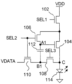
[0033] Figure 1 A illustrates an example of a pixel circuit along with its
control signal
25 lines to which a pixel driving scheme in accordance with an embodiment of
the
present invention is applied. The pixel circuit 100 of Figure lA includes
transistors
102-110, a storage capacitor 112 and an OLED 114. The pixel circuit 100 is
connected to three select lines SELL, SEL2, and SEL3, a signal line VDATA, a
voltage line VDD, and a common ground.
-5-
CA 02557713 2006-09-13
[0034] The transistors 102-I 10 may be amorphous silicon, poly silicon, or
organic
thin-film transistors (TFT) or standard NMOS in CMOS technology. It would be
appreciated by one of ordinary skill in the art that the pixel circuit 100 can
be
rearranged using p-type transistors.
s [0035] The transistor I04 is a driving transistor. The source and drain
terminals of
the driving transistor 104 are connected to the anode electrode of the OLED
114 and
the source terminal of the transistor 102, respectively. The gate terminal of
the
driving transistor 104 is connected to the signal line VDATA through the
transistor
110 and is connected to the source terminal of the transistor 106. The drain
terminal
i o of the transistor I06 is connected to the source terminal of the
transistor 102 and its
gate terminal is connected to the select line SEL2.
[0036] The drain terminal of the transistor 108 is connected to the
source~terminal of
the transistor I 10, its source terminal is connected to the anode of the OLED
114, and
its gate terminal is connected to the select line SEL3.
t 5 [0037] The drain terminal of the transistor 110 is connected to the signal
line
VDATA, and its gate terminal is connected to the select line SEL2.
[0038] The driving transistor 104, the transistor 106 and the storage
capacitor 112 are
connected at node A1. The transistors I08 and I IO and the storage capacitor
112 are
connected at node B 1.
20 [0039] Figure IB illustrates an example of a method of operating the pixel
circuit 100
of Figure 1 A. The pixel circuit 100 of Figure 1 A includes n-type
transistors.
However, it would be understood by one of ordinary skill in the art that the
method of
Figure IB is applicable to a pixel circuit having p-type transistors.
[0040] Referring to Figures 1 A-1 B, the operation of the pixel circuit 100
includes two
2a operating cycles: programming cycle 120 and driving cycle 122. At the end
of the
programming cycle 120, node A1 is charged to (VP+VT+QVOLED) where Vp is a
programming voltage, VT is the threshold voltage of the transistor 104, and
aVo~ED is
the OLED voltage shift under bias stress.
_g_
CA 02557713 2006-09-13
[0041 ] The programming cycle 120 includes two sub-cycles: pre-charging P 11
and
compensation P12, hereinafter referred to as pre-charging sub-cycle PI 1 and
compensation sub-cycle P12, respectively.
[0042] During the pre-charging sub-cycle P 1 I , the select lines SEL 1 and
SEL2 are
S high and SEL3 is low, resulting in turning the transistors 102, 106 and 110
on, and the
transistor 108 off respectively. The voltage at VDATA is set to (VOLEDI-VP).
"Vp" is
a programming voltage. "i" represents initial voltage of OLED. "VOLEDI" is a
constant voltage and can be set to the initial ON voltage of the OLED 114.
However,
VoLEDi can be set to other voltages such as zero. At the end of the pre-
charging sub-
to cycle Pl I, the storage capacitor 112 is charged with a voltage close to
(VDD+VP-
VOLEDI~.
[0043] During the compensation sub-cycle P12, the select line SEL2 is high so
that
the transistors 106 and 110 are on, and the select lines SELL and SEL3 are low
so that
the transistors 102 and 108 are off. As a result, the storage capacitor I 12
starts
t s discharging through the transistor 104 and the OLED 114 until the current
through the
driving transistor 104 and the OLED I I4 becomes close to zero. Consequently,
the
voltage close to (VT+VP+VOLED-VOLEDI~ is stored in the storage capacitor 1 I2
where
VOLED 1S the ON voltage of the OLED 114.
[0044] During the driving cycle 122, the select line SEL2 is low so that the
transistors
20 106 and 110 are off, and the select lines SEL 1 and SEL3 are high so that
the
transistors 102 and 108 are on. As a result, the storage capacitor 112 is
disconnected
from the signal line VDATA and is connected to the source of the driving
transistor
104.
[004] If the driving transistor 104 is in saturation region, a current close
to K(V~+
25 OVOI_ED~~ goes through the OLED I 14 until the next programming cycle where
K is
the trans-conductance coefficient of the driving transistor 104, and
dVoLeD=VOLED-
VOLEDI.
[0046] Figure 2 illustrates an example of a simulation result for the
operation of
Figures 1 A-1 B. The graph of Figure 2 represents OLED current during the
driving
cycle 122 as a function of shift in its voltage. Referring to Figures l A, I B
and 2, it
CA 02557713 2006-09-13
can be seen that as OVo~EO increases over time, the driving current of the
OLED 114
is also increased. Thus, the pixel circuit 100 compensates for luminance
degradation
of the OLED 114 by increasing the driving current of the OLED 114.
[0047] Figure 3 illustrates an example of another simulation result for the
operation of
s Figures lA-1B. The graph of Figure 3 represents OLED current during the
driving
cycle 122 as a function of shift in the threshold voltage of the driving
transistor 104.
Referring to Figures 1 A, 1 B and 3, the pixel circuit 100 compensates for
shift in the
threshold voltage of the driving transistor 104 since the driving current of
the OLED
114 is independent of the threshold of the driving transistor 104. The result
as shown
I 0 in Figure 3 emphasizes the OLED current stability for 4-V shift in the
threshold of the
driving transistor.
[0048] Figure 4A illustrates an example of a pixel circuit along with its
control signal
lines to which the pixel driving scheme in accordance with another embodiment
of the
present invention is applied. The pixel circuit 130 of Figure 4A includes five
i 5 transistors 132-140, a storage capacitor 142 and an OLED 144. The pixel
circuit 130
is connected to two select lines SELL and SEL2, a signal line VDATA, a voltage
line
VDD, and a common ground.
[0049] The transistors 132-140 may be same or similar to the transistors 102-
110 of
Figure lA. The transistors 132-140 may be amorphous silicon, poly silicon, or
organic
20 TFT or standard NMOS in CMOS technology. The storage capacitor 142 and the
OLED 140 are same or similar to the storage capacitor 112 and the OLED 114 of
Figure 1 A, respectively.
[0050] The transistor 134 is a driving transistor. The source and drain
terminals of
the driving transistor 134 are connected to the anode electrode of the OLED
144 and
3s the source of the transistor 132, respectively. The gate terminal of the
driving
transistor 134 is connected to the signal line VDATA through the transistor
140, and
is connected to the source terminal of the transistor 136. The drain terminal
of the
transistor 136 is connected to the source terminal of the transistor 132 and
its gate
terminal is connected to the select line SEL2.
_g_
CA 02557713 2006-09-13
[0051] The drain terminal of the transistor 138 is connected to the source
terminal of
the transistor 140, its source terminal is connected to the anode of the OLED
144, and
its gate terminal is connected to the select line SELL.
[0052] The drain terminal of the transistor 140 is connected to the signal
line
VDATA, and its gate terminal is connected to the select line SEL2.
[0053] The driving transistor 134, the transistor 136 and the storage
capacitor 142 are
connected at node A2. The transistors 138 and 140 and the storage capacitor
142 are
connected at node B2.
[0054] FigL~re 4B illustrates an example of a method of operating the pixel
circuit 130
of Figure 4A. The pixel circuit I30 of Figure 4A includes n-type transistors.
However, it would be understood by one of ordinary skill in the art that the
method of
Figure 4B is applicable to a pixel circuit having p-type transistors.
[0055] Referring to Figures 4A-4B, the operation of the pixel circuit 130
includes two
operating cycles: programming cycle 150 and driving cycle 152. At the end of
the
programming cycle 150, node A2 is charged to (VP+VT+~VOLED) where VP is a
programming voltage, Vr is the threshold voltage of the transistor 134, and
OVOLED 1S
the OLED voltage shift under bias stress.
[0056] The programming cycle 150 includes two sub-cycles: pre-charging P21 and
compensation P22, hereinafter referred to as pre-charging sub-cycle P21 and
compensation sub-cycle P22, respectively.
[0057] During the pre-charging sub-cycle P21, the select lines SEL1 and SEL2
are
high, and VDATA goes to a proper voltage VOLEDI that turns off the OLED 144.
Vo~E~i is a predefined voltage which is less than minimum ON voltage of the
OLEDs.
At the end of the pre-charging sub-cycle P21, the storage capacitor 142 is
charged
?5 with a voltage close to (VDD+Vo~EDi). The voltage at VDATA is set to
(VOLEDI-VP)
where Vr~ is a programming voltage.
[0058] During the compensation sub-cycle P22, the select line SEL2 is high so
that
the transistors 136 and I40 are on, and the select line SELL is low so that
the
transistors I32 and 138 are off. The voltage of VDATA at P22 is different from
that
-9-
CA 02557713 2006-09-13
of P21 to properly charge A2 to (VP~'VT"~QVOLeD) at the end of P22. As a
result, the
storage capacitor 142 starts discharging through the driving transistor 134
and the
OLED 144 until the current through the driving transistor 134 and the OLED 144
becomes close to zero. Consequently, the voltage close to ~VT+VP+VOLED-VOLEDI~
is
s stored in the storage capacitor 142 where Vo~EO is the ON voltage of the
OLED 144.
[0059] During the driving cycle 152, the select SEL2 is low, resulting in
turning the
transistors 136 and 140 off. The select line SEL1 is high, resulting in
turning the
transistors 132 and 138 on. As a result, the storage capacitor 142 is
disconnected
from the signal line VDATA and is connected to the source terminal of the
driving
transistor 134
[0060] If the driving transistor 134 is in saturation region, a current close
to K(VP+
~VOLED~~ goes through the OLED 144 until the next programming cycle where K is
the trans-conductance coeff cient of the driving transistor 134, and
~Vo~eo=Vo~eD-
Vo~e~i. As a result, the driving current of the OLED 144 increases, as the
OVo~Eo
~ 5 increases over time. Thus. the pixel circuit 130 compensates for luminance
degradation of the OLED 144 by increasing the driving current of the OLED 144.
[0061 J Moreover, the pixel circuit 130 compensates for shift in threshold
voltage of
the driving transistor 134 and so the driving current of the OLED 144 is
independent
of the threshold Vi~.
20 [0062] Figure SA illustrates an example of a pixel circuit along with its
control signal
lines to which the pixel driving scheme in accordance with a further
embodiment of
the present invention is applied. The pixel circuit 160 of Figure SA includes
six
transistors 162-172. a storage capacitor 174 and an OLED 176. The pixel
circuit 160
is connected to two select lines.SELI and SEL2. a signal line VDATA, a voltage
line
25 VDD, a bias current line IBIAS, and a common ground.
[0063] The transistors 162-172 may be amorphous silicon, poly silicon, or
organic
TFT or standard NMOS in CMOS technology. The storage capacitor 174 and the
OLED 176 are same or similar to the storage capacitor 112 and the OLED 114 of
Figure 1 A, respectively.
CA 02557713 2006-09-13
[0064] The transistor 164 is a driving transistor. The source and drain
terminals of
the driving transistor I 64 are connected to the anode electrode of the OLED
176 and
the source terminal of the transistor 162, respectively. The gate terminal of
the
driving transistor 164 is connected to the signal line VDATA through the
transistor
170 and is connected to the source terminal of the transistor 166. The drain
terminal
of the transistor 166 is connected to the source terminal of the transistor
162 and its
gate terminal is connected to the select line SEL2.
[0065] The drain terminal of the transistor 168 is connected to the source
terminal of
the transistor I70, its source terminal is connected to the anode of the OLED
176, and
its gate terminal is connected to the select line SEL1.
[0066] The drain terminal of the transistor 170 is connected to VDATA, and its
gate
terminal is connected to the select line SEL2.
[0067] The drain terminal of the transistor 172 is connected to the bias line
IBIAS, its
gate terminal is connected to the select Line SEL2, and its source terminal is
connected
t 5 to the source terminal of the transistor 162 and the drain terminal of the
transistor 164.
[0068] The driving transistor 164, the transistor 166 and the storage
capacitor 174 are
connected at node A3. The transistors 168 and 170 and the storage capacitor
174 are
connected at node B3.
[0069] Figure 5B illustrates an example of a method of operating the pixel
circuit 160
20 of Figure SA. The pixel circuit 160 of Figure SA includes n-type
transistors.
However, it would be understood by one of ordinary skill in the art that the
method of
Figure SB is applicable to a pixel circuit having p-type transistors.
[0070] Referring to Figures SA-SB, the operation of the pixel circuit 160
includes two
operating cycles: programming cycle 180 and driving cycle 182. At the
beginning of
35 the second operating cycle I 82. node A3 is charged to (VP+VT+QVOLeD) where
VP is a
pro~,~ramming voltage, VT is the threshold voltage of the transistor 164, and
OVOLED 1S
the OLED voltage shift under bias stress. VT and ~Vo~EO are generated by large
IBIAS resulting in a fast programming.
CA 02557713 2006-09-13
[0071] During the first operating cycle 180, the select line SEL1 is low, the
select line
SEL2 is high, and VDATA goes to a proper voltage (VOLEDI-VP) where VP is a
programming voltage. This proper voltage is a predefined voltage which is less
than
minimum ON voltage of the OLEDs. Also, the bias line IBIAS provides bias
current
(referred to as IBLaS) to the pixel circuit 160. At the end of this cycle node
A3 is
charged to VBlAS+VT+VOLED(IBf.aS) where Vsia,s is related to the bias current
IaiAS, and
VOLED(IBLaS) is the OLED 176 voltage corresponding to Iams. Voltage at node A3
is
independent of VP at the end of 180. Charging to (VP+VT+OVoLeD) happens at the
beginning of 182.
to [0072) During the second operating cycle 182, the select line SELL is high
and the
select line SEL2 is low. As a result node B3 is charged to Vot.EO(IP) where
VOLED(IP) is
the OLED 176 voltage corresponding to the pixel current. Thus, the gate-source
voltage of the transistor 164 becomes (VF+ OVOLED+VT) where
OVOLED=VOLED(IBIAS)-
Vo~EOi. Since the OLED voltage increases for a constant luminance while its
luminance decreases, the gate-source voltage of the transistor 164 increases
resulting
in higher OLED current. Consequently, the OLED 176 luminance remains constant.
[0073] Figure 6 illustrates an example of a display system 200 including the
pixel
circuit 100 of Figure lA. The display array 202 of Figure 6 includes a
plurality of
pixel circuit 100 arranged in rows and columns, and may form an active matrix
organic light emitting diode (AMOLED) display. VDATAj (j=1, 2, ...)
corresponds
to VDATA of Figure lA. SELIk, SEL2k and SEL3k (k=1, 2, ...) correspond to
SEL1, SEL2 and SEL3 of Figure lA, respectively. The select lines SELIk, SEL2k
and SEL3k are shared among the pixels in the common row of the display array
202.
The signal line VDATAj is shared among the pixels in the common column of the
?5 display array 202.
[0074] The display system 200 includes a driving module 204 having an address
driver 206, a source driver 208, and a controller 210. The select lines SELIk,
SEL2k
and SEL3k are driven by the address driver 206. The signal line VDATAj is
driven
by the source driver 208. The controller 210 controls the operation of the
address
3o driver 206 and the source driver 208 to operate the display array 202.
CA 02557713 2006-09-13
[0075) The waveforms shown in Figure 1B are generated by the driving module
204.
The driver module 204 also generate the programming voltage. The compensation
for
OLED degradation, threshold voltage shift and ground bouncing occur in pixel.
During the third cycle ( 122 of Figure 1 B), the gate-source voltage of the
driving
transistor is defined by the voltage stored in the storage capacitor (112 of
Figure 1).
Therefore, the ground bouncing does not change the gate-source voltage and so
the
pixel current become stable.
[0076] Figure 7 illustrates an example of a method of operating the display
array of
Figure 6. In Figure 7, Row(i) (i=I, 2, ...) represents a row of the display
array 202 of
to Figure 6. "120" and "122" in Figure 7 represent "programming cycle" and
"driving
cycle'' and correspond to those of Figure 1B, respectively. ''P11" and "P12"
in Figure
7 represent ''pre-charging sub-cycle'' and ''compensation sub-cycle" and
correspond to
those of Figure 1B, respectively. The compensation sub-cycle P1 I in a row and
the
pre-charging sub-cycle P 12 in an adjacent row are performed in parallel.
Further,
during the driving cycle 122 in a row, the compensation sub-cycle P22 is
performed in
an adjacent row. The display system 200 of Figure 6 is designed to implement
the
parallel operation, i.e., having capability of carrying out different cycles
independently
without affecting each other.
[0077] Figure 8 illustrates an example of a display system 300 including the
pixel
2o circuit 130 of Figure 4A. The display array 302 of Figure 8 includes a
plurality'of
pixel circuit 130 arranged in rows and columns, and may form an AMOLED
display.
VDATAj (j=l, 2, ...) corresponds to VDATA of Figure 4A. SELlk and SEL2k (k=l,
2, . . . ) correspond to SEL l and SEL2 of Figure 4A, respectively. The select
lines
SELIk and SEL2k are shared among the pixels in the common row of the display
array 302. The signal line VDATAj is shared among the pixels in the common
column of the display array 302.
[0078] The display system 300 includes a driving module 304 having an address
driver 306, a source driver 308, and a controller 3I0. The select lines SELIk
and
SEL2k are driven by the address driver 306. The signal line VDATAj is driven
by the
3o source driver 308. The controller 310 controls the operation of the address
driver 306
and the source driver 308 to operate the display array 302.
CA 02557713 2006-09-13
[0079] The waveforms shown in Figure 4B are generated by the driving module
304.
The driver module 304 also generates the programming voltage. The compensation
for OLED degradation, threshold voltage shift and ground bouncing occur in
pixel.
During the third cycle (I ~2 of Figure =1B). the gate-source voltage of the
driving
transistor is defined by the voltage stored in the storage capacitor (142 of
figure 4A).
Therefore, the ground bouncing does not change the gate-source voltage and so
the
pixel current become stable.
[0080] Figure 9 illustrates an example of a method of operating the display
array of
Figure 8. In Figure 9, Row(i) (i=l, 2, ...) represents a row of the display
array 302 of
Figure 8. "150" and "152'" in Figure 9 represent "programming cycle" and
"driving
cycle" and correspond to those of Figure 4B, respectively. ''P21" and "P22" in
Figure
9 represent "pre-charging sub-cycle" and ''compensation sub-cycle" and
correspond to
those of Figure 4B, respectively. The compensation sub-cycle P21 in a row and
the
pre-charging sub-cycle P22 in an adjacent row are performed in parallel.
Further,
l5 during the driving cycle 152 in a row, the compensation sub-cycle P22 is
performed in
an adjacent row. The display system 300 of Figure 8 is designed to implement
the
parallel operation, i.e., having capability of carrying out different cycles
independently
without affecting each other.
[0081 ] Figure 10 illustrates an example of a display system 400 including the
pixel
2o circuit 160 of Figure SA. The display array 402 of Figure 10 includes a
plurality of
pixel circuit 160 arranged in rows and columns, and is an AMOLED display. The
display array 402 may be an AMOLED display. VDATAj (j=1, 2, ...) corresponds
to
VDATA of Figure 4A. IBIASj (j=1, 2, ...) corresponds to IBIAS of Figure 4A.
SELIk and SEL2k (k=1, 2, ...) correspond to SELI and SEL2 of Figure 4A,
25 respectively. The select lines SEL 1 k and SEL2k are shared among the
pixels in the
common row of the display array 402. The signal line VDATAj and the bias line
IBIASj are shared among the pixels in the common column of the display array
402.
[0082] The display system 400 includes a driving module 404 having an address
driver 406, a source driver 408, and a controller 410. The select lines SEL 1
k and
30 SEL2k are driven by the address driver 406. The signal line VDATAj and the
bias
line IBIASj are driven by the source driver 408. The controller 410 controls
the
CA 02557713 2006-09-13
operation of the address driver 406 and the source driver 408 to operate the
display
array 402.
[0083] The waveforms shown in Figure SB are generated by the driving module
404.
The driver module 404 also generate the programming voltage. The compensation
for
OLED degradation, threshold voltage shift and ground bouncing occur in pixel.
During the second cycle 182 of Figure SB, the gate-source voltage of the
driving
transistor is defined by the voltage stored in the storage capacitor (174 of
Figure SA).
Therefore, the ground bouncing does not change the gate-source voltage and so
the
pixel current become stable.
[0084] Figure 11 illustrates an example of a method of operating the display
array of
Figure 10. In Figure 9, Row(i) (i=1, 2, ...) represents a row of the display
array 402 of
Figure 10. "180" and "182"' in Figure I 1 correspond to those of Figure SB,
respectively. For the rows of the display array 402, the programming cycle I
80 is
subsequently performed. During the driving cycle I 82 in a row, the
programming
~ s cycle 180 is performed in an adjacent row. The display system 400 of
Figure 10 is
designed to implement the parallel operation, i.e., having capability of
carrying out
different cycles independently without affecting each other.
[0085] All citations are hereby incorporated by reference.
[0086] The present invention has been described with regard to one or more
2o embodiments. However, it will be apparent to persons skilled in the art
that a number
of variations and modifications can be made without departing from the scope
of the
invention as defined in the claims.
-~5-