Note: Descriptions are shown in the official language in which they were submitted.
CA 02557714 2006-08-28
WO 2005/091784 PCT/US2005/003707
hENS ARRAY AND METHOD OF MAKING SAME
BACKGROUND
Field of the Invention
The present invention relates generally to microlens
arrays and optical lenses, and more particularly to methods
for manufacturing microlens arrays or non-spherical lenses.
Related Art
Microlens arrays provide optical versatility in a
miniature package for imaging appli rations. Traditionally, a
microlens is defined as a lens with a diameter less than one
millimeter; however, a lens having a diameter as large as
five millimeters or more has sometimes also been considered
a microlens.
There are many conventional methods for manufacturing
microlens arrays, such as using reflow or diffusion. Figs.
lA-1C show a typical sequence of steps for making a
microlens array by depositing material, patterning, and
reflowing. In Fig. 1A, a photosensitive layer 10, such as a
photosensitive resin, is formed on a planari~ation layer 12
over a silicon substrate (not shown). The material of the
photosensitive layer is used to form the microlens array.
In Fig. 1B, photosensitive layer 10 is patterned to form an
array of shapes, such as rectangles, stripes, or squares 14,
where the shapes are located where the individual
microlenses will be formed. Patterning, for example, can be
with a conventional mask and photoresist process, where a
photoresist is deposited on photosensitive layer 10, exposed
through a mask having opaque areas, developing (or removing)
selected portions of the photoresis t, and etching areas of
photosensitive layer 10 left expose d by the photoresist.
1
CA 02557714 2006-08-28
WO 2005/091784 PCT/US2005/003707
Squares 14 are then heated sufficiently to cause them to
reflow, thereby forming an array of semi-spherical
microlenses 16, as shown in Fig. 1C.
However, microlens arrays made by thermal reflowing, as
described above, have several disadvantages. Typically,
photosensitive resins contain components which absorb
proportionally more light in the blue region of the visible
spectrum. As a result, the color spectrum is distorted,
producing an image that is more "yellowish" than it should
be. This color distortion increases with time due to
oxidation of the resin. Another disadvantage is that the
resolution with which the photosensitive resin can be
patterned is limited by the thickness of the resin layer.
The thicker the resin layer, the farther apart the
microlenses in the array, which reduces the light collection
efficiency of the array. On the other hand, the resin layer
must be thick enough so that, when reflowed, the sag of the
resultant microlenses is sufficient to cause the desired
focusing effect. Consequently, it is difficult to obtain
the highest possible collection efficiency with microlens
arrays fabricated in this manner. Yet another disadvantage
results from the fact that as the curvature radius of the
microlens becomes small, the incident light is focused on a
point near the microlens. Thus, the photosensitive layer is
patterned to be square or rectangular in shape according to
the shape of a cell, using a mask that is simply divided
into opaque regions and light-transmissive regions, and is
thermally treated to form a microlens. Thus, a curvature
radius of the microlens is decreased. Moreover, because a
microlens formed in a rectangular shape has a significant
difference between its curvature radius in the width and the
length directions, it is difficult to focus incident light
on the corresponding photodiode without error, and a part of
the light is focused on the planarization layer or color
2
CA 02557714 2006-08-28
WO 2005/091784 PCT/US2005/003707
filter layer between the photodiode and the microlens,
causing loss of light and deterioration of sensitivity and
resolution.
Another conventional method of forming microlens arrays
is by diffusion, such as described in "Light Coupling
Characteristics of Planar Microlens", by M. Oikawa et al.,
Proc. SPIE, 1544, 1991, pp. 226-237, which is incorporated
by reference in its entirety. Figs. 2A-2G show steps for
forming a microlens array using two types of diffusion. In
Fig. 2A, a glass substrate 20 is provided. In Fig. 2B, a
metal film 22 is deposited on glass substrate 20. Metal
film 22 is then patterned, such as with conventional
processes, to remove portions 24 where individual
microlenses are to be formed, as shown in Fig. 2C. Figs. 2D
and 2E show one type of further processing, where the
exposed areas 24 are diffused with an appropriate dopant and
energy (Fig. 2D) and then the remaining metal is removed and
the surface is polished, such as with a chemical or machine
polish, to form microlenses 26 (Fig. 2E). Figs. 2F and 2G
show another type of further processing, where ions,
protons, or other suitable molecules are used to bombard
(e. g., with low energy) (Fig. 2F) and diffuse into substrate
20 and the remaining metal portions removed and the
irradiated portions "swelled" (Fig. 2G), such as with an
organic vapor, to form microlenses 28. The result is a high
numeral aperture planar microlens array. One disadvantage
to forming microlens arrays using diffusion is that control
of the thickness along the optical axis is limited.
Microlens arrays are typically used with an underlying
array of sensors, such as complementary metal oxide
semiconductor (CMOS) or charge couple device (CCD) sensors,
to form an imaging device. The microlenses collect and
focus light onto corresponding sensors. The microlenses
3
CA 02557714 2006-08-28
WO 2005/091784 PCT/US2005/003707
significantly improve the light sensitivity of the imaging
device by collecting light from a large light collecting
area and focusing it on a small light sensitive area of the
sensor (i.e., pixel). One conventional method of generating
an image signal is shown in Fig. 3. Light rays 30 are
collected and focused by a microlens layer 32 comprising an
array of microlenses 34 overlying a planarization layer 36,
such as formed by processes described above. After passing
through planarization layer 36, light rays 30 are filtered
by color filters 38 in a filter layer 40, with each color
filter allowing only light of a specific color to pass, such
as red, green, and blue (RGB). Light through the filters
are then passed through a sensor layer 42, comprising an
array of sensors 44, such as photodiodes or CCD devices. A
processor (not shown) combines signals from the sensors to
create a color image.
Such an arrangement of microlenses, filters, and
sensors has several disadvantages. Several processing steps
are needed to form the separate microlens layer 32, filter
layer 40, and sensor layer 42, which increase cost and time.
The layers also increase the separation between the
microlenses and the sensors, which can increase crosstalk
between pixels, due in part to light impinging on adjacent
sensors instead of the desired sensor.
In addition to microlenses, high quality non-spherical
lenses are also critical components to many applications in
the imaging field. They are widely used in optical systems
for controlling critical light propagation and correcting
image color quality, such as in professional cameras and
video imaging equipment. However, the fabrication of non-
spherical lenses is complicated and can only be done through
skilled manual operation by highly trained professionals.
Unlike spherical lenses which can be manufactured quickly by
4
CA 02557714 2006-08-28
WO 2005/091784 PCT/US2005/003707
using conventional machines, non-spherical or specially
sized or shaped lenses are typically shaped and polished
manually and frequently individually. This can be time
consuming and costly.
Accordingly, there is a need for an improved lens,
microlens, or array and method of manufacturing such,
including non-spherical lenses, that overcomes the
disadvantages of conventional lens arrays or non-spherical
lenses and related processes, such as described above.
Further, there is a need for an integrated microlens array
and sensor array that overcomes the disadvantages as
described above with conventional microlens/sensor devices.
SUMMARY
The present invention provides improved microlens
arrays or non-spherical lenses and processes of forming
microlens arrays or non-spherical lenses. In one aspect,
the microlens array is formed on a sensor array, resulting
in an integrated microlens/sensor device.
According to one embodiment, an array of sensors is
first fabricated on a substrate. A dielectric layer, such.
as a spin-on polymer (e. g., polyimide) or an oxide (e. g.,
Si02) is deposited over the sensor array. A patterning
photosensitive dielectric layer, such as a spin-on
photoresist, is next formed over the dielectric layer.
Selected portions of the patterning layer are removed to
expose areas of the dielectric layer overlying the
individual sensors where microlenses are to be formed. The
exposed portions are then processed to form curved recesses,
such as by using a wet etch, a grey-scale mask, or a shadow
mask. The curved recesses may have a controlled shape and
range from a shallow recess to a deep spherical recess,
depending on the desired characteristics of the microlens.
CA 02557714 2006-08-28
WO 2005/091784 PCT/US2005/003707
Remaining portions of the patterning layer are then removed.
An inorganic lens material having a higher refractive index
than the underlying dielectric layer, such as Si02, SiOXNy,
Si3N4, Ti02, or a polymer, is deposited over the dielectric
layer to form an integrated array of microlenses and
sensors. The layer of lens material may be polished, if
desired.
In other embodiments, the dielectric layer can be
deposited over any substrate and does not have to be a
sensor array. In such embodiments, the process forms and/or
can be used to make plastic molding templates to form
individual spherical or non-spherical lenses, or an array of
spherical and/or non-spherical microlenses of any desired
shape or shapes. The process of the present invention
allows a lens or microlens array to be formed with different
shaped non-spherical and/or spherical lenses. This gives
the lens manufacturer more flexibility to fabricate many
additional types of lens arrays at discount prices.
The present invention provides numerous advantages over
conventional microlens arrays and methods. Since the
microlens array is formed directly onto the sensor array
with fewer processing steps than conventional methods,
microlens/sensor devices of the present invention are easier
and less expensive to fabricate than conventional devices.
The focal length of the microlenses can be controlled
depending on the type of dielectric materials used for the
microlenses and/or process control (i.e., curvature of the
lens elements.)
The present invention also provides improved sensor
sensitivity due to the ability to make non-spherical lenses
using wet etching, grey-scale mask or shadow mask
processing. Another advantage is that using non-organic
lens materials extends the reliability or useful lifetime of
6
CA 02557714 2006-08-28
WO 2005/091784 PCT/US2005/003707
the microlens. The color quality of the image produced by
the sensor is also improved because the lens material does
not have the adverse characteristics of resin-containing
materials, which as discussed above, can absorb
proportionally more blue light to make the image yellowier
than desired. Yet another advantage the current invention
provides is that the resulting microlens/sensor device is
thinner and more resistant to environmental effects because
the microlens array acts as a protection layer for the
sensor elements.
The resulting microlens array may be used with devices
for a variety of application, from a small display screen
for a camera, a digital camera sensor, a personal digital
assistant, or a laptop to a large display screen for a
projection screen, a wall-sized display screen, or a
billboard-sized display screen. The processing or
fabrication of the array/sensor unit allows high throughput
with consistent characteristics between each array/sensor
unit.
The scope of the invention is defined by the claims,
which are incorporated into this section by reference. A
more complete understanding of embodiments of the present
invention will be afforded to those skilled in the art, as
well as a realization of additional advantages thereof, by a
consideration of the following detailed description of one
or more embodiments. Reference will be made to the appended
sheets of drawings that will first be described briefly.
BRIEF DESCRIPTION OF THE DRAWINGS
Figs. 1A-1C show a typical sequence of steps for making
a microlens array by reflowing according to a conventional
process;
7
CA 02557714 2006-08-28
WO 2005/091784 PCT/US2005/003707
Figs. 2A-2E show steps for forming a microlens array
using one type of diffusion according to a conventional
process;
Figs. 2A-2C and 2F-2G show steps for forming a
microlens array using another type of conventional process;
Fig. 3 shows one type of conventional microlens array
and sensor array device;
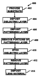
Fig. 4 is a flow chart showing a process for
fabricating a microlens array onto a sensor array according
to one embodiment of the present invention;
Figs. 5A-5G show various stages of a process for
fabricating a microlens/sensor array according to one
embodiment;
Figs. 6A and 6B show a grey scale mask and
characteristic of a grey scale mask, respectively, for use
in one embodiment of the invention;
Figs. 7A-7C show various stages of a process for
forming controlled curvature recesses using a grey scale
mask according to one embodiment; and
Fig. 8 is an angled view of a microlens array according
to one embodiment of the present invention.
Embodiments of the present invention and their
advantages are best understood by referring to the detailed
description that follows. It should be appreciated that
like reference numerals are used to identify like elements
illustrated in one or more of the figures.
DETAILED DESCRIPTION
Fig. 4 is a flowchart illustrating a method 400 in
accordance with an embodiment of the present invention for
8
CA 02557714 2006-08-28
WO 2005/091784 PCT/US2005/003707
fabricating a microlens array or a non-spherical lens. A
substrate is first provided in step 402, where the substrate
may include an array of CMOS or CCD sensors. The sensor
array may be any suitable size, ranging from small screen
applications to large display devices. A dielectric layer
is then deposited on the substrate in step 404. A
patterning layer, such as a spin-on photoresist or other
photosensitive material, is deposited on the dielectric
layer in step 406. Selected portions of the patterning
layer are removed, such as by conventional photolithography
processing, in step 408. The removed portions expose areas
of the dielectric layer where the microlenses or non-
spherical lenses are to be formed. With embodiments having
a sensor array, the exposed areas correspond to locations of
individual sensor elements.
In step 410, the exposed portions of the dielectric
layer are selectively etched, such as with a wet etch, a
grey scale mask, or shadow mask, to form controlled curved
recesses. The curved recesses deepest in the center and
taper up toward the sides or circumference. The etching
does not remove all the dielectric material such that the
underlying substrate or sensors are exposed. Further, the
curved recesses can be any suitable shape, such as semi-
spherical or non-spherical, depending on the application.
The remaining portions of the patterning layer are removed
in step 412, and the resulting template is ready for further
processing steps or can be used for plastic molding of
specially designed lenses. When the template is to be
continued for further processing, a layer of inorganic lens
material is deposited over dielectric layer, in step 414, to
fill in the curved recesses. The lens material, in one
embodiment, has a refractive index higher than that of the
dielectric layer. Examples of suitable lens materials
include, but are not limited to, Si02, SiOXNY, Si3N4, Ti02, a
9
CA 02557714 2006-08-28
WO 2005/091784 PCT/US2005/003707
polymer, or plastics in the case of plastic molding. The
layer of lens material may then be polished if necessary.
Figs. 5A-5G show various stages of fabricating a
microlens array according to one embodiment of the
invention. Fig. 5A shows a top view of a substrate 500 onto
which the microlens array will be formed. In one
embodiment, substrate 500 is a glass or silicon substrate,
in which the resulting device is a microlens array. In
another embodiment, substrate 500 is a sensor array formed
on top of a supporting substrate, such as glass or silicon,
in which the resulting device is an integrated
sensor/microlens array. The sensor array can be an array of
a
CMOS or CCD sensors, such as photodiodes or other sensor
elements. Fabrication of the sensor array is with
conventional methods. Fig. 5A shows the embodiment where a
sensor array 502 with individual sensor elements 504 is
formed on a supporting substrate 506. A dielectric layer
508, such as an oxide (e. g. , Si02, Ti02) , nitride (e. g. ,
SiOXNy), spin-on polymer, is deposited on sensor array 502,
as shown in Fig. 5B. The thickness of the dielectric layer
508 depends on specific application requirements. In one
embodiment for integrated sensor/microlens array, dielectric
layer 508 is between 1 ~m and several millimeters thick. In
another embodiment for individual non-spherical lens,
dielectric layer 508 can be up to one centimeter or thicker.
Next, in Fig. 5C, a patterning layer 510 is deposited
over dielectric layer 508, where patterning layer 510 will
be used to expose portions of the dielectric layer where
microlenses or non-spherical lenses will be formed.
Patterning layer 510 is a photosensitive dielectric material
and is selected based on the type of patterning process
used. For example, for a photolithography process,
patterning layer 510 can be a spin-on photoresist or other
CA 02557714 2006-08-28
WO 2005/091784 PCT/US2005/003707
photos ensitive material. The desired pattern can then
formed on patterning layer 510 by exposure through a
photomask. The photomask, if the photoresist is positive,
may have an array of circular openings, where the circular
openings correspond to locations of the microlenses to be
formed. If the microlenses are to have different shapes
and/or sizes, the individual openings of the photomask can
be adjusted accordingly. Exposed portions of patterning
layer 510 are then removed to expose portions 512 of
dielectric layer 508 where microlenses or non-spherical
lenses are to be formed, as shown in Fig. 5D. With an
underlying sensor array, portions 512 correspond to
indiv.z.dual sensor elements 504.
In Fig. 5E, exposed portions 512 of dielectric layer
508 are then etched to form curved recesses 514 overlying
sensor elements 504. Curved recesses 514 can be semi-
spher.ical, as shown in Fig. 5F, which is a top view of Fig.
5E. As noted above, the shape of individual curved recesses
514 can be varied according to the microlens application.
Furthe r; curved recesses 514 are formed, in one embodiment,
by controlled etches, such as a wet etch or etching after
patte ruing using a grey scale mask or shadow mask. Other
etching processes for tapered etching may also be suitable
with the present invention. The depth and taper of the etch
also determines the optical characteristics, such as focal
length, of the microlens or lens. Thus, by controlling the
etch of the dielectric layer, different types of microlens
arrays can be easily fabricated.
Figs. 6A and 6B and 7A-7C show a method of forming
contr oiled curved recesses using a grey scale mask process
according to one embodiment. Fig. 6A shows an example of
one opening 600 of a grey scale mask, where a typical grey
scale mask will have many such openings 600 separated by
11
CA 02557714 2006-08-28
WO 2005/091784 PCT/US2005/003707
opaque sections in between. A grey scale mask lets
different amounts of light through different radius
locations of the opening, such as shown in Fig. 6B. The
degree of grey at different radii of the opening 600 on the
grey scale mask determines the degree of light exposure at
corresponding locations of the underlying photosensitive
dielectric such as photoresist. As shown, less light passes
through radially outward from the center of the opening,
from a maximum of approximately 1000 at the center to
approximately 0% at the edge or outer circumference. The
light transmission curve "a" can be any suitable shape for
forming the desired microlens or lens.
Figs. 7A-7C show a sequence of steps using a grey scale
mask to form the controlled curved recesses. In Fig. 7A, a
small portion of patterning layer 510 (such as a positive
photoresist) is exposed through one opening 600 of a grey
scale mask. Note that the portions between openings of the
grey scale mask in the x-direction are opaque. Patterning
layer 510 is developed and a dry etch is performed to
transfer the exposed pattern to underlying dielectric layer
508, as shown in Figs. 7B and 7C, to form curved recesses
514. Thus, by controlling the scale of the grey on the grey
scale mask and dry etch, both spherical and non-spherical
microlenses and lenses of different designs can be formed
quickly and inexpensively.
Depending on the type of patterning and etch, curved
recesses 514 may need to be treated to smooth out
irregularities on the surface of the curved recesses. The
"roughness" of the curved recesses should be small compared
to the wavelength of the visible light. In one embodiment,
the roughness should be approximately 1/10 the wavelength of
the visible light. "Roughness" as defined herein refers to
the distance or variation between peaks and troughs on the
12
CA 02557714 2006-08-28
WO 2005/091784 PCT/US2005/003707
surface of the curve d recesses. For example, when using dry
etch to form curved recesses 514, a quick wet etch or wash
may be added to smooth out any roughness of the surface of
curved recesses 514. An alternative to the quick wet etch
is to coat the surface of curved recesses 514 with a thin
dielectric material of the same refractive index as
underlying dielectri c layer 508. Other suitable methods to
smooth out the surface areas of the recesses 514 include
those such as proper 1y designed chemical mechanical
polishing (CMP) and the like.
After forming curved recesses 514 of dielectric layer
508 (and polished if necessary), the structure can be used
as a template for ma king plastic lenses through plastic
molding, or to continue further processing for
microlens/sensor integration. For plastic molding of
lenses, multiple templates of the same pattern design and
curved shapes or different design and shapes may be used
depending on specifi c applications. When used for
microlens/sensor integration, referring back to Fig. 5G,
after curved recesse s 514 of dielectric layer 508 are formed
(and polished if necessary), a layer of transparent lens
material 516 is depo sited, as shown in Fig. 5G, to form the
microlens array. In one embodiment, the lens material is
inorganic and has a higher index of refraction than that~of
underlying dielectri c layer 508. Some suitable materials
for lens material 51 6 include dielectrics, such as Si02,
SiOXNy, Si3N4, Ti02, a polymer, plastics or a combination of
them. Thus, depending on the microlens requirements,
dielectric layer 508 and lens material 516 are selected
accordingly. In one embodiment, the deposited thickness of
lens material 516 is approximately the same as the depth at
the center of the curved recesses or thicker depending on
the application requirement. Use of inorganic lens
materials, as opposed to resin-based reflow processes,
13
CA 02557714 2006-08-28
WO 2005/091784 PCT/US2005/003707
produces lenses that create a truer color image. That is,
there is no extra absorption in the blue spectrum, which
produces yellowier images. Further, forming the microlens
by deposition instead of diffusion provides better control
of the lens shape and the thickness along the optical axis.
After deposition of lens material 516, the upper surface can
be polished to produce a flat smooth surface if necessary.
Fig. 8 is an angled view of a microlens array 800
having integrated sensors/microlenses. Transparent lens
material 516 can act as a protection layer for the
underlying microlenses 802 and sensor array 502. Each
microlens 802 corresponds to an underlying sensor element
808, which are supported by substrate 506. Light entering
microlens array 800 is directed toward individual sensors in
the sensor array by corresponding microlenses 802. The
process of making the microlens array allows more light to
be received by the sensors, thereby improving image
sensitivity and color quality. However, as noted above,
microlens array 800 or an individual non-spherical lens does
not require an underlying array of sensors.
The present invention allows a microlens array or
individual lens having non-spherical or different
sized/shaped microlenses/lens to be manufactured easily. In
conventional processes for making non-spherical or specially
sized or shaped lenses, the lenses are typically shaped and
polished manually and sometimes individually. This can be
costly in terms of time and effort. On the other hand,
spherical lens arrays can be manufactured quickly by using
conventional machines. However, the machines do not allow
non-spherical lenses to be formed nor do they allow lenses
of different shapes or sizes to be formed on the same array.
Advantageously, the present invention allows microlens
arrays or lenses having non-spherical microlenses or lenses
14
CA 02557714 2006-08-28
WO 2005/091784 PCT/US2005/003707
of different shapes or sizes to be made quickly and
inexpensively.
Embodiments described above illustrate but do not limit
the invention. It should also be understood that numerous
modifications and variations are possible in accordance with
the principles of the present invention. For example, the
above embodiments describe the use of a patterning layer
over a dielectric laye r. However, the dielectric layer can
be excluded if the pat terning photosensitive dielectric
layer can be directly used to form usable curved recesses or
to form the curved recesses using other means such as
suitable chemical pros esses or ion beam sputtering and the
like. Accordingly, th a scope of the invention is defined
only by the following claims.