Note: Descriptions are shown in the official language in which they were submitted.
CA 02558774 2007-04-10
Image Display Apparatus Which Corrects Pre-Stored Pixel Correction Data
This is a division of copending Canadian Patent Application Serial
Number 2,313,550, filed July 6, 2000.
BACKGROUND OF THE INVENTION
The present invention relates to a display apparatus provided with a
plurality of light emitting devices such as light emitting diodes arrayed in a
matrix display panel, and to its method of operation.
Today, bright red, green, and blue (RGB) light emitting diodes (LEDs) of
1000mcd or more have been developed, and fabrication of large-scale LED
displays has become possible. These LED displays have features such as low
power consumption, lightness in weight, and the possibility for thin panel
display. Further, demand for large-scale displays, which can be used out
doors,
has increased dramatically.
Practical large-scale LED displays are configured to fit the installation
space by assembling a plurality of LED units. An LED unit is formed from a dot
matrix array of RGB LEDs arranged on a substrate board.
Further, an LED display is provided with a driver circuit capable of
driving each individual light emitting diode. Specifically, each LED control
device, which transmits display data to each LED unit, is connected to the LED
display, and a pluraiity of LED units are connected to form one large-scale
LED
display. The number of LED units used increases as the LED display becomes
larger in scale. For example, a large-scale display can use 300 vertical x 400
horizontal, or 120,000 LED units.
The LED display uses a dynamic driver system as its driver method, and
specifically, the display is connected and driven as described below.
CA 02558774 2000-07-06
For example, in an mxn dot matrix LED unit, each LED anode in each
line is connected to a common source line, and each LED cathode in each
column is connected to a common current line. The m-line common source lines
are sequentially turned on for display with a prescribed period. For example,
m-
line common source line switching is performed via decoder circuitry based on
the address signal.
However, when LEDs connected to a selected common source line were
activated in related art apparatus, charge accumulated in non-activated LEDs
connected to unselected common source lines. When these common source
lines were then selected, excess current developed as a result of charge built-
up
during their inactive period. As a result of this problem, LEDs controlled to
be off
emitted low levels of light and sufficient image contrast could not be
obtained.
These types of effects caused display quality degradation.
Thus, the first object of the present invention is to reduce the effects of
accumulated charge and provide a high quality image display apparatus and its
method of operation.
Further, in an LED display, corrected image data are typically used for
each LED device to display a high quality image. This is because device-to-
device LED variation in brightness, for example, is relatively large.
More specifically, the control circuit has a read-only-memory (ROM)
correction data memory section to store correction data corresponding to each
LED device. Corrected image data based on the correction data stored in ROM
has been used for display.
However, since correction data were stored in ROM in related art
apparatus, correction data could not be re-written. Consequently, related art
apparatus had the problem that it was necessary to provide a re-writable
memory device separate from ROM when different correction data were
required.
Thus, the second object of the present invention is to provide an image
display apparatus which can store a plurality of correction data in one
correction
2
CA 02558774 2000-07-06
data memory section.
Further, to accurately represent image data on an LED display, the light
emission characteristics (driving current vs. brightness characteristics) of
each
LED device in the image display apparatus must be uniform. However, since
LEDs are fabricated on wafers by semiconductor technology, light emission
characteristic variation results from fabrication lot-to-lot, wafer-to-wafer,
and
chip-to-chip. Therefore, it is necessary to correct image data amplitude to
compensate for light emission characteristic differences of the LED for each
pixel.
An example of related art image data correction is described as follows.
Turning to Fig. 12, a block diagram of an embodiment of a related art
LED display is shown. In Fig. 12, 101 is an m-line n-column LED matrix, 107 is
a
control circuit, 105 is a microprocessor unit (MPU), 106 is a ROM to store
correction data, 102 is a common driver circuit, 103 are horizontal driver
circuits,
109 are correction circuits to correct image data, and 110 are random access
memory (RAM) to temporarily store correction data. The horizontal driver
circuits
103, correction circuits 109, and RAM 110 are integrated in LED driver
integrated circuits (IC's) 104 (k) provided for each column of the LED matrix
(k=1
to n).
First, prior to display illumination, correction data for the mxn pixels
stored in ROM are transferred to a high speed buffers. RAM 110 are used as the
high speed buffers. Correction data transfer is accomplished as follows.
First,
correction data held in ROM 106 are read out by the MPU 105. The MPU 105
sequentially selects LED driver IC's 104 (k) via the address bus 111 and
sequentially outputs one columns-worth, or m-pixels, of correction data
corresponding to each selected column. The correction data output is input to
each LED driver IC 104 (k) via the correction data bus 112 and stored in RAM
110 internal to the LED driver IC 104 (k).
When LEDs are illuminated, correction data stored in RAM 110 are
sequentially read out by correction circuits 109. The value of input image
data
CA 02558774 2000-07-06
(IMDATA) is increased or decreased for each pixel based on the correction data
to achieve image data correction. Corrected image data are output to the
driver
circuits 103, and the driver circuits 103 produce driving current for each LED
based on the corrected image data.
However, in the related art LED display described above, a total of mxn
pixels-worth of correction data must be stored in the buffers, or RAM 110, and
as
display pixel count increases, very large RAM capacity becomes necessary.
Further, the operation of correction data read-out from RAM 110 to the
correction circuits 109 becomes complicated as the amount of RAM increases.
In addition to these problems, both the address bus 111 and the data bus 112
must branch to, and connect with each of the n driver IC's 104 (1 to n) making
wiring complex and peripheral circuitry large in area.
Thus, the third object of the present invention reflects consideration of
these problems, and is to provide an image display apparatus which can reduce
the amount of data stored in the buffers, and can accomplish image data
correction with a simple circuit structure.
The above and further objects and features of the invention will more
fully be apparent from the following detailed description with accompanying
drawings.
SUMMARY OF THE INVENTION
The image display apparatus of the present invention is provided with a
dot matrix of light emitting devices, driver circuitry, and a switching
circuit
section. The dot matrix is a plurality of light emitting devices arranged in a
matrix
of m-lines and n-columns. One terminal of each light emitting device in each
column is connected to a current line, and the other terminal of each light
emitting device in each line is connected to a common source line. Driver
circuitry controls display drive active or inactive depending on an input
illumination signal. In the display drive active state, driver circuitry
controls
4
CA 02558774 2000-07-06
connection of one end of each common source line and each current line
according to input display data. The switching circuit section floats the
other end
of each common source line in the active state and connects the other end of
all
common source lines to ground in the inactive state.
In this image display apparatus, charge accumulated at light emitting
devices and their periphery in the active state, is discharged via the
switching
circuit section during the inactive state. Consequently, the effects of charge
accumulated during active illumination of prescribed light emitting devices
are
essentially eliminated, and a high quality image display apparatus is
realized.
In the image display apparatus of the present invention, driver circuitry
can be configured as m-units of current source switching circuits connected to
respective common source lines, and a constant current control circuit
section.
In the active state, a current source switching circuit connects a current
source
to the common source line selected by an input address signal. The constant
current control circuit section is provided with memory circuits, and these
memory circuits store pixel level data for n-pixels of sequentially input
display
data. In the active state, the constant current control circuit section drives
a
current line for the pixel level width corresponding to pixel level data
stored in
the memory circuit.
Further, the present invention is a method of operation of an image
display apparatus provided with a plurality of light emitting devices arranged
in a
dot matrix of m-lines and n-columns, wherein one terminal of each light
emitting
device in each column is connected to a current line, and the other terminal
of
each light emitting device in each line is connected to a common source line.
This method of operation is characterized by inclusion of a step to control
active
and inactive states according to an illumination control signal which controls
the
state of illumination, a step to control conduction through one end of each
common source line and one end of each current line in the active state based
on input display data, and a step to float the other end of each common source
line in the active state and ground the other end of each common source line
in
5
CA 02558774 2000-07-06
the inactive state.
In image display apparatus method of operation of the present invention,
charge accumulated at light emitting devices and their periphery in the active
state, can be discharged via the switching circuit section during the inactive
state. Consequently, the effects of charge accumulated during active
illumination of prescribed light emitting devices can essentially be
eliminated,
and a high quality image display apparatus method of operation can be offered.
Further, the image display apparatus of the present invention is
provided with a display section of light emitting devices arrayed in an m-line
by
n-column matrix, a correction data memory section to store correction data
corresponding to each respective light emitting device, and control and driver
circuitry to correct input image data based on the correction data and to
display
an image on the display section using the corrected image data. The correction
data memory section is provided with a single memory unit having a read-only
first memory bank, which holds pre-stored first correction data, and a
writable
second memory bank.
An image display apparatus of this structure can retain first correction
data in the first memory bank without erasure, and can use the writable second
memory bank to store second correction data, which are different than the
first
correction data. Depending on requirements, either the first correction data
or
the second correction data can be selected to revise the image data. In the
image display apparatus of the present invention, the correction data memory
section can be configured using non-volatile memory which is electrically
erasable and writable.
The image display apparatus of the present invention may also be
provided with a communication control section. The communication control
section can allow writing of second correction data, which are different than
first
correction data, to the second memory bank, and forbid writing to the first
memory bank. It is also desirable to be able to set the writable second memory
bank to forbid writing and protect correction data written into that memory
bank.
6
CA 02558774 2000-07-06
In the correction data memory section of the image display apparatus of
the present invention, it is desirable to store correction data for each pixel
such
that the address corresponds to the light emitting device for each pixel, and
the
first memory bank and the second memory bank can be distinguished by the
highest order address bit. In this manner, lower order address bits can be set
for
the same read-out address independent of memory bank.
Further, it is desirable to configure the image display apparatus
described above in units which display one part of the entire image data. In
this
manner, the entire image of a large-scale display can easily be assembled from
a plurality of these display units.
Further, the image display apparatus of the present invention is
provided with:
(a) a display section made up of a plurality of light emitting devices
arranged in an m-line by n-column matrix;
(b) a vertical driver section which sequentially selects each line of the
display section and sources current to each line;
(c) a horizontal driver section which supplies driving current to each
column of the display section according to image data corresponding to the
selected line;
(d) an image data correction section which corrects externally input
image data according to variations in light emitting device characteristics
for
each pixel, and outputs corrected data to the horizontal driver section; and
(e) a correction data memory section to hold correction data for image
data correction.
The image data correction section reads out one line of correction data
from the correction data memory section each time it outputs one line of
corrected image data to the horizontal driver section. In this system, the
amount
of correction data that must be temporarily retained in the image data
correction
section can be reduced, large amount of memory such as random access
memory (RAM) does not need to be used as buffer memory, and image data can
7
CA 02558774 2000-07-06
be corrected via simple circuit structure.
The image data correction section of the image display apparatus of the
present invention is provided with buffer memory to store at least one line of
correction data. The image data correction section can read out the next line
of
correction data from the correction data memory section while it outputs one
line
of corrected image data to the horizontal driver section. This prevents any
display time lag between lines due to image data correction.
In the image display apparatus of the present invention, shift registers
can be provided as buffer memory, and correction data can be read via the
shift
registers by direct sequential shifting one bit at a time. This eliminates the
need
for data bus line branching to transfer correction data to buffer memory in
the
correction data memory section, and it also eliminates the need for an address
bus to select buffer memory. Therefore, wiring area can be reduced and wiring
layout options can be increased.
Still further, in the image display apparatus of the present invention, two
stages of interconnected registers can be provided as buffer memory. When the
first register outputs one line of correction data, the next line of
correction data is
read into the second register. Each time output and input of one line of
correction data is completed, correction data from the second register can be
transferred to the first register. With this system, image data can be
corrected
with a simple circuit structure.
In the image display apparatus described above, the second register
can be a shift register, and correction data can be read by direct sequential
shifting one bit at a time. This eliminates the need for data bus line
branching to
transfer correction data, and it also eliminates the need for an address bus
to
select buffer memory.
The image display apparatus of the present invention can use LEDs as
the light emitting devices. In this image display apparatus, LED display
peripheral circuit structure can be simplified and the display apparatus can
made compact.
4
CA 02558774 2000-07-06
Finally, the image display apparatus of the present invention can display
images by dividing the entire image into parts. Since the image display
apparatus of the present invention can simplify peripheral circuit structure,
it is
suitable for use in image data units which display part of an entire image,
for
example, it is suitable for LED units used in large-scale LED displays.
In accordance with one aspect of the present invention, there is
provided an image display apparatus comprising: (a) a display section of
LEDs, which are the pixel elements, arranged in an m-Iine by n-column matrix;
(b) a correction data memory section which stores correction data
corresponding to the LED for each respective pixel, is provided with a first
memory bank which forbids writing to memory and holds pre-stored first
correction data, and is provided with a second memory bank which allows
writing to memory; and (c) control and driver circuitry which corrects input
image data based on the correction data and displays an image on said display
section using the corrected image data.
BRIEF DESCRIPTION OF THE DRAWINGS
The present invention taken in conjunction with the invention disclosed
in copending Canadian Patent Application Serial Number 2,313,550, filed July
6, 2006, will be discussed in detail hereinbelow with the aid of the
accompanying drawings wherein:
Fig. 1. is a conceptual drawing showing the structural format of the
image display apparatus of an embodiment of the present invention.
Fig. 2. is a block diagram showing a specific example of the image
display apparatus shown in Fig. 1.
Fig. 3. is a block diagram showing another specific example of the
image display apparatus.
Fig. 4 is a timing diagram showing common source driver and switching
circuitry control for the image display apparatus shown in Fig. 3
Fig. 5. is a conceptual drawing showing the structural format of the
image display apparatus of another embodiment of the present invention.
9
CA 02558774 2000-07-06
Fig. 6. is a block diagram showing a specific example of the image
display apparatus shown in Fig. 5.
Fig. 7. is a block diagram showing the detailed structure of an electrically
erasable programmable ROM (EEPROM) and serial communication interface
for the specific example of Fig. 6.
Fig. 8. is a conceptual drawing showing the structural format of the
image display apparatus of another embodiment of the present invention.
Fig. 9. is a block diagram showing a specific example of the image
display apparatus shown in Fig. 8.
Fig. 10. is a timing diagram showing correction data transmission timing
for the image display apparatus shown in Fig. 9.
Fig. 11 is an abbreviated drawing showing the relation between control
9a
CA 02558774 2000-07-06
line number and ROM read-out beginning address for the image display
apparatus shown in Fig. 9.
Fig. 12. is a block diagram showing the circuit structure for a related art
image display apparatus.
DETAILED DESCRIPTION OF THE INVENTION
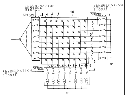
Fig. 1 is a conceptual drawing illustrating an image display apparatus
provided with a switching circuit section to discharge accumulated charge in
the
dot matrix. The display apparatus of Fig. 1 is provided with an LED dot matrix
10,
a current source switching circuit 1, a constant current control circuit
section 3,
and a switching circuit section 2. The display apparatus of Fig. 1 uses LEDs
as
light emitting devices, but devices other than LEDs may also be used as the
light
emitting devices.
(1) The LED dot matrix 10 is a plurality of LEDs 4 arranged in an m-
line, n-column matrix. The cathode of each LED 4 in each column is connected
to a current line 6. The anode of each LED 4 in each line is connected to a
common source line 5.
(2) The current source switching circuit 1 is provided with m-switching
circuits which correspond to, and are connected to each respective common
source line 5. The current source switching circuit 1 connects a current
source to
the common source line 5 selected by the address signal for the illumination
period specified by the input illumination control signal. This supplies
current to
the LEDs 4 connected to the selected common source line 5.
(3) The constant current control circuit section 3 is provided with
memory circuits to store n-sets of sequentially input pixel level data. The
constant current control circuit section 3 drives the current lines with a
pixel level
width, corresponding to the pixel level data stored in each memory circuit,
over
the time interval specified by the input illumination control signal.
(4) The switching circuit section 2 floats the opposite end of each
I O
CA 02558774 2000-07-06
common source line over the illumination time interval of the input
illumination
control signal, and grounds the opposite end of each common source line during
the off interval (non-illumination interval) of the input illumination control
signal.
In a display apparatus with the above configuration, on-off switching of
the current source switching circuit 1, the constant current control circuit
section
3, and the switching circuit section 2 are all performed according to the
illumination control signal. During the illumination interval of the
illumination
control signal, the current source switching circuit 1 and the constant
current
control circuit section 3 are activated, while the switching circuit section 2
is
deactivated (each switch connected to the opposite end of a common source
line is off). When activated, the current source switching circuit 1 connects
a
common source line selected by the input address signal to the current source.
At this time, the constant current control circuit section 3 drives the
current lines
with a pixel level width corresponding to pixel level data stored in each
memory
circuit. In this manner, LEDs 4 connected to the common source line selected
by
the address signal are illuminated with the pixel level width corresponding to
the
associated pixel level data. Further, in the deactivated state, both the
current
source switching circuit 1 and the constant current control circuit section 3
are
deactivated, while the switching circuit section 2 is activated. Consequently,
during off intervals indicated by the illumination control signal, charge
accumulated by each LED or its associated connections is discharged to ground
via each closed switch in the switching circuit section 2. Therefore, each LED
and its associated connections do not accumulate charge under these
conditions.
Subsequently, illumination intervals and off intervals are sequentially
repeated. LEDs disposed in each line are sequentially illuminated during each
illumination interval, and the desired image is displayed on the LED dot
matrix.
With this system, charge accumulated by LEDs (or their associated
connections) which are not illuminated during an illumination interval, is
discharged during the next off interval. Consequently, during the illumination
ll
CA 02558774 2000-07-06
interval, LED illumination can be controlled with each LED and its associated
connections always in a discharged state with no unwanted charge build-up.
Accordingly, the display apparatus of Fig. 1 can obtain sufficient image
contrast, and high quality display is possible. This is because illumination
control can be accomplished without the effects of charge accumulation.
Turning to Fig. 2, the following describes a specific configuration of the
display apparatus of the present invention. In Fig. 2, items which are the
same
as those in Fig. 1 are labeled with the same part number.
As shown in Fig. 2, the current source switching circuit 1 of this specific
embodiment comprises a decoder circuit 11 and common source drivers 12.
When the illumination control signal is in a digital signal low state (LOW),
the
decoder circuit 11 controls the common source drivers 12 on or off for current
source connection to the common source line 5 selected by the address signal.
When the illumination control signal is in a digital signal high state (HIGH),
the
current source switching circuit 1 controls the common source drivers 12 via
the
decoder circuit 11 to disconnect all common source lines from the current
source.
When the illumination control signal is LOW, this type of current source
switching circuit 1 connects only the common source line 5 of the LED dot
matrix
10 selected by the address signal to the current source.
The constant current control circuit section 3 is provided with a shift
register 31, memory circuits 32, a counter 33, data comparitors 34, and a
constant current driver section 35. In this type of constant current control
circuit
section 3, pixel level data are shifted n-times by the shift register in
synchronization with a shift clock. Pixel level data corresponding to each of
the
n-current lines are clocked into, and stored in respective memory circuits 32
in
response to a latch clock signal. When the illumination control signal is LOW,
the output signal from data comparitors 34 is input to the constant current
driver
section 35. The data comparitors compare pixel level data with the value
output
from a counter 33 clocked by a pixel level reference clock used as the counter
12
CA 02558774 2000-07-06
clock. The constant current driver section 35 controls the flow of constant
current in each current line for a driver pulse width interval corresponding
to the
pixel level data value.
As described above, the current source switching circuit 1 and the
constant current control circuit section 3 perform LED display pixel level
control
when the illumination control signal is LOW. When the illumination control
signal
is HIGH, the LED dot matrix is not connected to the current source switching
circuit 1 or the constant current control circuit section 3.
When the illumination control signal is HIGH, the switching circuit
section 2 turns on switches to ground all common source lines 5. When the
illumination control signal is LOW, switches are turned off to disconnect
(float)
all common source lines 5.
The display apparatus of Fig. 2 configured as described above drives
the LED dot matrix 10 with constant current to illuminate prescribed LEDs when
the illumination control signal is LOW. When the illumination control signal
is
HIGH, constant drive of the LED dot matrix 10 is suspended. In this state,
accumulated residual charge in each LED of the LED dot matrix 10 and its
associated connections is discharged via the switching circuit section 2.
The embodiment of Fig. 2 described above is organized to drive the LED
dot matrix 10 with constant current when the illumination control signal is
LOW,
and to turn the switching circuit section 2 on when the illumination control
signal
is HIGH. However, the present invention is not restricted to this system, and
control may also be performed with the LOW level and HIGH level reversed.
Turning to Fig. 3, another embodiment of the image display apparatus of
the present invention is shown. Elements of Fig. 3 which are the same as those
of Figs. 1 and 2 are labeled with the same part number. The image display
apparatus shown in Fig. 3 is provided with a switching decoder circuit 13,
which
separately controls each switch SW1 -6 of the switching circuit section 2. the
switching decoder circuit 13 controls each switch SW1 -6 of the switching
circuit
section 2 ON and OFF based on input signals such as the address signal and
13
CA 02558774 2000-07-06
the illumination control signal. When the illumination control signal is logic
HIGH,
the switching decoder circuit 13 controls only the switch selected by the
address
signal ON to ground only the common source line connected to that switch. At
this time, all remaining switches not selected by the address signal are OFF,
and all remaining common source lines connected to those switches are left
floating.
The timing diagram of Fig. 4 shows display apparatus control for the
current source switching circuit 1 common source drivers 12 and for each
switch
SW1-6 of the switching circuit section. The common lines 1-6 shown in Fig. 4
are the common source lines connected to the corresponding switches SW1-6
of the switching circuit section 2.
As shown in Fig. 4, when the illumination control signal is logic LOW,
the current source switching circuit 1 controls the common source drivers 12
to
connect only the common source line 5 selected by the address signal to the
current source. Further, when the illumination control signal is logic HIGH,
the
switching decoder circuit 13 turns only the switch selected by the address
signal
ON to ground that common source line. For example, when the address signal is
0 and the illumination control signal is LOW, common line 1 is controlled ON,
and the current source is connected only to that common source line. At this
time,
all the switches SW1-6 are controlled OFF. Next, when the address signal is 0
and the illumination control signal goes HIGH, common line 1 is controlled
OFF,
in addition only SW1 connected to the other end of common line 1 is controlled
ON, and only that common source line is grounded. When an illuminated LED
goes to the inactive state (not illuminated), the switching decoder circuit 13
immediately controls the switching circuit section 2 to ground the common
source line connected to that LED. This is done to effectively prevent
accumulation of charge when an illuminated LED is turned OFF.
In the manner described above, common source lines 1-6 and switches
SW1-6 are selected according to the address signal, and the selected common
source lines and switches are controlled ON or OFF by LOW and HIGH logic
14
CA 02558774 2000-07-06
levels of the illumination control signal. By successive repetition of LED
illumination and common source line grounding this image display apparatus
displays a prescribed image on the LED dot matrix. In this display apparatus,
only the switch connected to the selected common source line is turned ON.
Therefore, low level current flow through unselected line LEDs is reliably
prevented, and low level illumination of these unselected LEDs can be
prevented.
Fig. 5 is a block diagram showing the overall conceptual structure of an
image display apparatus provided with a correction data memory section
comprising a read-only first memory bank and a writable second memory bank.
The image display apparatus of Fig. 5 is provided with a display section 21 of
light emitting devices arrayed in an m-line by n-column matrix, a correction
data
memory section 26 to store correction data corresponding to each respective
light emitting device, and control and driver circuitry to correct input image
data
based on the correction data and to display an image on the display section 21
using the corrected image data. The control and driver circuitry is provided
with
a vertical driver section 22, a horizontal driver section 23, image data
correction
section 24, control section 25, image data input section 27, communication
control section 28, and buffer memory 20. In this image display apparatus,
image data input to the image data input section 27 are transferred to the
control
section 25.
The correction data memory section 26 connected to the control section
has a first memory bank and a second memory bank. For example, the
correction data memory section 26 may be an EEPROM (non-volatile memory in
25 which data can be electrically erased or re-written). First correction
data, such
as data to correct brightness variation for each pixel are stored in the first
memory bank. Second correction data are stored in the second memory bank.
In the present embodiment, brightness variation correction data are
used as an example of correction data, but the present invention is not
restricted
to this type of correction data.
IS
CA 02558774 2000-07-06
The image data correction section 24 corrects image data for each pixel
input via the image data input section 27 and the control section 25 according
to
first correction data or second correction data for each respective pixel
input
from the control section 25 and buffer memory 20. The image data correction
section 24 outputs this corrected data to the horizontal driver section 23 as
pixel
level data corresponding to each pixel. The buffer memory 20 for this image
display apparatus embodiment has (1) through (n) memory units 20
corresponding to each of 1 through n columns.
The horizontal driver section 23 is provided with n memory units
corresponding to each of the n columns. Input pixel level data corresponding
to
each pixel are stored in memory provided for the column containing that pixel.
The horizontal driver section 23 drives a prescribed current line for the
pixel
level width corresponding to the pixel level data stored in memory in response
to
a control signal from the control section 25.
Further, the vertical driver section 22 is provided with m-switching
circuits connected to each of the m-common source lines. The vertical driver
section 22 connects a current source to a specified common source line
according to a control signal from the control section 25.
As described above, the control section 25 reads first correction data or
second correction data from the correction data memory section 26 and stores
the data in buffer memory 20. The control section 25 also controls data input-
output timing for buffer memory 20 and the image data correction section 24.
The control section 25 also controls switching to connect common source lines
with the current source in the vertical driver section 22. Finally, the
control
section 25 controls switching to drive current lines in the horizontal driver
section 23. In this manner, the control section 25 sequentially illuminates
each
pixel in the display section 21 and displays an image corresponding to the
input
image data on the display section 21.
In particular, the image display apparatus of the present embodiment
has the following features.
I6
CA 02558774 2000-07-06
(1) The correction data memory section 26 is provided with a first
memory bank containing pre-stored first correction data corresponding to each
pixel, and a second re-writable memory bank.
(2) The image display apparatus is provided with a communication
control section 28. The communication control section 28 allows writing of
second correction data, which are different than first correction data, to the
second memory bank, and forbids writing to the first memory bank.
(3) The control section 25 can select either first correction data stored
in the first memory bank or second correction data stored in the second memory
bank, and store it in buffer memory 20.
Consistent with these features, the image display apparatus of Fig. 5
can use the re-writable second memory bank to store second correction data,
which are different than first correction data, while avoiding erasure of
first
correction data retained in the first memory bank. Consequently, it is
possible to
correct image data depending on requirements by selecting either first
correction data or second correction data.
Embodiment (brightness correction data two bank correction control
circuit, Fig. 6)
The following describes an embodiment of the image display apparatus
of the present invention with reference to Fig. 6. The image display apparatus
of
the present embodiment is provided with an LED dot matrix 41 as the display
section, a common driver 42 as the vertical driver section, EEPROM 46 as the
correction data memory section, the correction circuit 49 of LED driver IC's
44 as
the image data correction section, the driver section 43 of LED driver IC's 44
as
the horizontal driver section, a command control section 47 and control
section
45 as the control section, a serial communication interface 48 as the
communication con'trol section, and the shift register 402 and register 401 of
LED driver IC's 44 as the buffer memory.
The command control section 47 inputs a common source line selection
signal, LINE ADR, to the common driver 42 and an illumination control signal,
17
CA 02558774 2000-07-06
BLANK, to each driver section 43 and correction circuit 49.
In the present embodiment, the EEPROM 46 comprises, for example, a
BANKO, in which correction data are written at the factory at shipping time,
and a
BANK1, in which the user can write correction data after shipping. The control
section 45 selects correction data from either BANKO or BANK1 in response to a
control signal from the serial communication interface 48. In this embodiment,
write-protect settings are made to forbid the user from re-writing data to
BANKO,
in which correction data are written at the factory at shipping time.
The serial communication interface 48 in this embodiment performs
various processing according to commands embedded in received signals.
Control of reading and writing to the EEPROM 46 is described below.
The following details EEPROM 46 structure and the serial
communication interface 48 configuration for controlling EEPROM 46 reading
and writing. As shown in Fig. 7, the serial communication interface 48 is
configured with a write-protect control section 48f comprising an address
register 48b, a control register 48e, and AND logic circuits 48c and 48d, in
addition to a command control 48a.
The input signal, RXD, to the serial communication interface 48 includes
commands, which instruct data to be written to the EEPROM 46 (write
commands), and writable communication data, which are input to the command
control section 48a. As shown in Fig. 7, the writable communication data
includes starting address data (Start Address in Fig. 7) specifying the
location to
write data to, and the data to be written (WRITE DATA in Fig. 7).
When an RXD input signal containing a write command is received by
the serial communication interface 48, the command control section 48a outputs
command data to remove write-protection (WP set-remove command data) to
the control register 48e. The command control section 48a also outputs the
highest order bit, A12, of the starting address data to the address register
48b,
and a logic 1 to the AND logic circuit 48c. Further, the command control
section
48a outputs the writable communication data to the address decoder 46a of the
18
CA 02558774 2000-07-06
EEPROM 46.
Here, when the highest order bit, A12, is 0, BANKO is indicated as the
ROM area to write to, and when the highest order bit, A12, is 1, BANK1 is
indicated as the ROM area to write to.
In the present invention, the EEPROM 46 may comprise two or more
memory banks. In the case of more than two memory banks, the highest order
two or more bits can be used to indicate the applicable memory bank.
The control register 48e is pre-set to the write-protect mode and
normally outputs a logic 0 indicating the write-protect mode to the AND logic
circuit 48d. However, when command data (WP set-remove command data)
indicating removal of write-protection are input from the command control
section 48a, a logic 1 indicating removal of write-protection is output to the
AND
logic circuit 48d.
When a logic 1 is input via the address register indicating BANK1, and
the control register 48e issues a logic 1 to remove write-protection, the AND
logic circuit 48d outputs a logic 1 to AND logic circuit 48c.
When the command control section 48a issues a logic 1 and a logic 1 is
input from AND logic circuit 48d, AND logic circuit 48c outputs a logic 1 to
the
XWP terminal of the EEPROM 46. At all other times the AND logic circuit 48c
outputs a logic 0. When a logic 1 is input to the XWP terminal of the EEPROM
46, write-protection is removed (WP-OFF). When a logic 0 is input to the XWP
terminal of the EEPROM 46, write-protection is maintained (WP-ON).
The XWP terminal is the write-protect terminal of the EEPROM 46 and
data writing is made valid or invalid at this terminal. When XWP=O (LOW), data
writing to the EEPROM is invalid and the write-protect mode is set. When
XWP=1 (HIGH), data writing to the EEPROM is valid and the write-protect mode
is not set.
Switching between BANKO and BANK1 at the EEPROM 46 is
accomplished by the address decoder 46a based on the highest order bit A12
contained in the writable communication data. Further, memory bank selection
19
CA 02558774 2000-07-06
for read-out is performed in the same manner as for data writing using the
highest order bit A12. Namely, memory bank selection can be performed by the
EEPROM 46 address decoder 46a based on the highest order bit A12 contained
in the writable communication data, which are input from the command control
section 48a.
In Fig. 7, an example of a 13 bit wide address bus is shown, but memory
bank selection by the highest order bit can be performed in the same manner
for
more than 13 bits or less than 13 bits.
In the EEPROM46 and serial communication interface 48 configuration
described above, EEPROM 46 BANKO correction data are always protected,
while BANK1 correction data can be re-written according to the RXD signal.
Further, either BANKO or BANK1 can be selected to read correction data from.
Control of the EEPROM 46 by direct connection of the serial
communication interface 48 was described above. However, the EEPROM 46
can be controlled in the same fashion by connection of the serial
communication
interface 48 to the EEPROM 46 via the intervening control section 45, as shown
in Fig. 6. Specifically, each control signal from the serial communication
interface 48 to the EEPROM 46 is simply input to the EEPROM 46 via the control
section 45 in the same fashion as for direct connection. Correction data read
from the EEPROM 46 are branched to the shift registers 402 of the LED driver
IC's 44 by the control section 45 connected between the EEPROM 46 and the
serial communication interface 48.
Further, the RXD signal received by the serial communication interface
48 may be input from an external controller (not illustrated). As shown in
Fig. 6,
data such as correction data read from the EEPROM 46 can be transmitted, for
example, to an external controller by the serial communication interface 48 as
the TXD signal.
In the display apparatus embodiment of Fig. 6 described above, image
data, the vertical synchronization signal, Vsync, and the horizontal
synchronization signal, Hsync, are input to the control section 47 via an
image
CA 02558774 2000-07-06
data input section (not illustrated). Input image data are transferred from
the
command control section 47 to the LED driver IC 44 correction circuits 49
Further, the vertical synchronization signal, Vsync, and the horizontal
synchronization signal, Hsync, are input to the control section 45, the
correction
circuit 49 and driver section 43 of each LED driver IC 44, and the common
driver
42.
The control section 45 controls each element of the display apparatus in
synchronization with the input vertical synchronization signal, Vsync, and
horizontal synchronization signal, Hsync. Further, correction data read from
the
EEPROM 46 BANKO or BANK1 depending on the input signal to the serial
communication interface 48, are sequentially transferred to the shift
registers
402 according to control section 45 instructions. After one lines-worth of
correction data are transferred to the shift registers 402, the data are input
to
respective correction circuits 49 via corresponding registers 401.
Specifically,
image data and correction data corresponding to that image data are input to
the
correction circuits 49.
Image data input to the correction circuits 49 are corrected by the
correction circuits 49 according to the correction data. The result is then
taken
as the pixel level data, and input to each driver section 43. Based on the
corrected image data (pixel level data), prescribed LED lines of the LED dot
matrix 41 are illuminated by the common driver 42 and each driver section 43
to
display an image according to the image data.
In the embodiment of the image display apparatus of present invention
described above, correction data stored in BANKO of the EEPROM 46, for
example, correction data written at the factory at shipping time, can be
retained
without erasure. The re-writable BANK1 can be used, for example, by the user
to
store correction data revised to account for the environment of operation.
Depending on requirements, it is possible to select either correction data set
to
correct the image data.
Further, in this configuration of the embodiment of the present invention,
21
CA 02558774 2000-07-06
a single memory device such as an EEPROM can be used instead of providing
two memory devices such as a ROM and an EEPROM. Therefore, the structure
can be made compact.
In this embodiment, an EEPROM 46 having a write-protect feature (WP
function) was described. Write versus read-only control can be achieved for an
EEPROM with no WP function by controlling the output state of the write-enable
control signal, XWE, which controls timing for EEPROM writing. For example,
for
the case of an active LOW write-enable pulse, XWE, when the serial
communication interface receives write commands in the write-protect mode, the
same write-protect feature can be achieved by setting XWE always to logic
HIGH.
Specifically, the present invention is not restricted to the structure of the
embodiment described above. It is sufficient if the system has at least one
correction data memory section, and that correction data memory section is
provided with a write-protected area and an area which can be written to.
For image display on a large-scale LED display of the present invention,
it is desirable to divide the overall image into parts and implement display
on
LED units. For example, a large-scale LED display, in which the user has
already set the second memory bank for specific operational conditions, may
require LED units in one part to be replaced. The second memory bank can be
re-written to adjust only for the replaced LED units, and re-adjustment for
the
user's operational conditions can be accomplished easily.
Again, the present invention is not restricted to an image display
apparatus using light emitting diodes.
Fig. 8 is a block diagram outlining a image display apparatus
embodiment having an image data correction section which reads one line of
correction data from the correction data memory section each time it outputs
one
line of corrected image data. The image display apparatus shown in Fig. 8 is
provided with:
(a) a display section 61 made up of a plurality of light emitting devices
22
CA 02558774 2000-07-06
arranged in an m-line by n-column matrix;
(b) a vertical driver section 62 which sequentially selects each line of
the display section 61 and sources current to each line;
(c) a horizontal driver section 63 which supplies driving current to
each column of the display section 61 according to image data corresponding to
the selected line;
(d) an image data correction section 64 which corrects externally input
image data (IMDATA) according to variations in light emitting device
characteristics for each pixel, and outputs corrected data to the horizontal
driver
section 63; and
(e) a correction data memory section 66 which holds correction data
for image data correction. Operation of each element of this system is
controlled
by a control section 65.
The image data correction section 64 reads correction data (CRDATA)
from the correction data memory section 66 via the control section 65,
corrects
image data (IMDATA) input via the control section 65 based on the correction
data, and outputs the corrected image data to the horizontal driver section
63. A
total of mxn pixels of correction data are not read all at once, but rather
correction data are read one line (n pixels) at a time in parallel with output
of one
line of image data.
For the case of image data for a static image, it is possible to correct the
image data without providing any buffer memory at all. However, for the case
of
image motion, buffer memory which can store one or two lines of correction
data
is desirable to prevent display time lag between lines. The buffer memory 60
can
be configured, for example, as two stages of interconnected registers 601 and
602.
Correction data reading may proceed, for example, in the following
manner. The image data correction section 64 is provided with buffer memory 60
made up of two stages (upper and lower) of interconnected registers 601 and
602. When the first register 601 outputs one line of correction data to the
23
CA 02558774 2000-07-06
correction circuit 69, the next line of correction data is read into the
second
register 602. When the first register 601 finishes outputting one line of
correction
data and the second register 602 finishes reading one line of correction data,
the contents of the second register 602 are transferred to the first register
601.
An array of D-flip-flops for just one display lines-worth of data (n-pixels
times the bit count for one pixel (a)) can be used, for example, as the first
register 601 and the second register 602. To simplify correction data input
wiring,
it is desirable to connect flip-flops of the second register 602 in a master-
slave
sequence to form a shift register. In this configuration, correction data
input to
the flip-flop at the left end of the second register 602 is sequentially
transferred
(shifted) to the right side in sync with clock (CLK) timing, and data are thus
read
into the second register 602. Therefore, bus line branching to each column for
correction data input is unnecessary, and wiring to supply a clock signal to
each
flip-flop is all that is required.
Fig. 9 is a block diagram showing detailed structure of the image display
apparatus shown in Fig. 8. First, the configuration of each section is
described.
An LED dot matrix 71, which is the display section, is made up of LEDs
arranged
in an m-line by n-column matrix. The anodes of all LEDs located in each line
are
connected to one common source line. The cathodes of all LEDs located in each
column are connected together on one current line. A common driver 72, which
is the vertical driver section, comprises a current switching circuit provided
with
m-switching circuits and related current source. The common driver 72 supplies
current to LEDs connected to a common source line by connecting the common
source line to the current source. Driver circuits 73, which are the
horizontal
driver section, comprise constant current control circuits which control
driving
current on and off to each column according to the pixel level width of image
data output from the correction circuits 79.
The image data correction section is made up of correction circuits 79,
which correct and output sequentially input image data one line at a time, and
registers 701 and shift registers 702, which are buffer memory to store
24
CA 02558774 2000-07-06
correction data. Each register 701 and shift register 702 have flip-flops
corresponding to the number of bits for one column of pixels. Further, each
flip-
flop of register 701 is connected to its corresponding flip-flop in shift
register 702.
The control section is made up of the control circuit 77 (CTL) and a direct
memory access controller (DMAC) 75. ROM 76, which is the correction data
memory section comprises memory such as EEPROM. Brightness correction
data to correct for brightness differences due to variation in the light
emission
characteristics of each LED in the LED dot matrix 71 are stored in ROM 76.
Correction data are data to control driving current to each LED according to
each pixel and each color. Data to control LED illumination time or a
combination of illumination time and driving current, instead of driving
current
alone, are also suitable data.
A driver circuit 73, correction circuit 79, register 701, and shift register
702 are provided for each column of the LED dot matrix 71, and are contained
within an LED driver IC (k) for each column (k=1 to n). Shift registers 702
for
each column are connected together to allow data shifting. Further, to reduce
the number of LED driver IC's, driver circuits, etc. for an appropriate number
of
columns can be combined into one LED driver IC.
Writing to, and reading from the correction data ROM 76 can be
performed independent from image data transmission via SCI 78, which is a
serial communication interface. Writing to the ROM 76 may also be performed
by direct connection to the ROM 76 using direct transfer methods, or via
various
types of interfaces and parallel buses. When data are to be written to the ROM
76 while correction data are being read from the ROM 76, data transfer by the
DMAC 75 is interrupted, and data reception through the SCI 78 is given
priority.
This allows control of competition for ROM 76 access.
The flow of image data in this type of embodiment proceeds as follows.
Image data (IMDATA) are input to the CTL 77 and distributed to the correction
circuits 79. After each line of image data is corrected by the correction
circuits
79, it is output to the driver circuits 73.
CA 02558774 2000-07-06
Next, the flow of correction data is described with reference to the timing
diagram of Fig. 10. For simplification, Fig. 10 illustrates the case of
illumination
of three common source lines #0 through #2 in that order.
Line #0 correction data begins to be read into the shift registers 702
when vertical and horizontal image timing data, Vsync and Hsync, are input to
the CTL 77. Vsync input to CTL 77 is transferred to the common driver 72 as
the
LINE ADR signal, and Hsync is transferred to the driver circuits 73 and the
correction circuits 79 as the BLANK signal.
(1) First, the CTL 77 inputs into DMAC 75 the starting address
(ADDRESS) for reading line #0 correction data from ROM 76. The DMAC 75
writes to ROM 76 via the data input-output bus DIO the starting address for
reading, while issuing a write-enable signal XWE to ROM 76. As outlined in
Fig.
11, the starting address for read-out from ROM 76 indicates the beginning
address of correction data within the ROM memory map corresponding to the
selected line. CTL 77 issues the starting address for reading correction data
corresponding to the line number determined from Vsync and Hsync.
(2) After writing the starting address for reading, the DMAC 75 reads
line #0 correction data from ROM 76 via the data bus DIO while issuing a read-
enable signal XOE. The ROM 76 sequentially outputs correction data
corresponding to the LOW pulse count on XOE.
(3) Line #0 correction data (CRDATA) read into DMAC 75 are
transferred to shift registers 702 within driver IC's 74 (k). Correction data
are
transferred sequentiaify into the shift registers 702 by shifting one bit at a
time in
synchronization with the clock CLK.
While line #0 correction data are being read into the shift registers 702,
registers 701 retain line #2, which is the last line, correction data. Line #2
correction data maintained in registers 701 are output to the driver circuits
73
and line #2 LEDs are illuminated while the correction data are maintained in
registers 701.
When the next Hsync pulse is input, a latch signal (LATCH) is issued
?6
CA 02558774 2000-07-06
from the DMAC 75 to the registers 701, line #0 correction data stored in the
shift
registers 702 are transmitted to registers 701 all at once, and line #0 LED
illumination is started. Subsequently, the starting address for reading line
#1
correction data is input from the CTL 77 to the DMAC 75. In the same manner
described above, the DMAC 75 reads line #1 correction data from ROM 76 and
writes it into the shift registers 702.
In this manner, while the previous line is being illuminated, input of data
to correct each pixel of the next line to be illuminated is completed.
Correction
data input to shift registers 702 are transmitted to, and retained in
registers 701
just before switching illumination from one line to the next. Based on this
retained correction data, the correction circuits 79 correct image data by
compensating for brightness variations in each LED of the active display line.
By
consecutive repetition of these operations, LED brightness correction is
achieved over the entire display.
Incidentally, transfer of correction data into shift registers 702 must be
completed within the time for illumination of one display line. Therefore, an
image display apparatus like a large screen LED display using LED units
without
too many image data bits per line is suitable for practical implementation of
data
transfer via shift registers.
Here, a serial EEROM, in which data are read-out in serial fashion, was
described as the ROM 76. However, an EEPROM with n-bit address and data
busses may also be used as the ROM 76. Further, correction data transfer
between the DMAC 75 and shift registers 702 was explained via a serial bus,
but
data transfer may also be performed via parallel bus.
For the case of a full color LED display, each pixel is made up of three
RGB color LEDs. Image data for each respective RGB color can be corrected in
the same manner as previously described.
The embodiments described above were presented as separate
embodiments to make each characteristic easy to understand. The image
display apparatus shown in Figs. 1 and 2 has a switching circuit section to
27
CA 02558774 2000-07-06
connect light emitting device common source lines to ground to discharge
accumulated charge. The image display apparatus shown in Figs. 5 and 6 is
configured with a correction data memory section having a first memory bank,
which stores first correction data and forbids writing to memory, and a second
memory bank which can be written to. In the image display apparatus shown in
Figs. 8 and 9, each time one line of corrected image data is output from the
image data correction section to the horizontal driver section, the next line
of
correction data is read from the correction data memory section. However, the
most ideal image display apparatus can be realized by an apparatus provided
with all of the circuitry described above.
As this invention may be embodied in several forms without departing
from the spirit of essential characteristics thereof, the present embodiment
is
therefore illustrative and not restrictive, since the scope of the invention
is
defined by the appending claims rather than by the description preceding them,
and all changes that fall within the meets and bounds of the claims, or
equivalence of such meets and bounds thereof are therefore intended to be
embraced by the claims.
28