Note: Descriptions are shown in the official language in which they were submitted.
CA 02558849 2006-09-06
' ~
A SYSTEM AND MI;TAOD FOR EXCLUDING NARROW BAND NOISI!: FROM
A COMMUNICATION CHANNEL
FIELD OF TFIir; INVENTION
[OOIJThe present invention relates generally to the field of communications.
More
specifically, tlye present invention relates to digital filtering of one or
mote
communication cloannels
BACICGROUND
j002J Degradation of signal-to-noise ratio ("SNR") as well as Bit energy to
noise ratio
("Eb/No") or Dit energy to interference ratio ("Eb/I") or Carrier to-
Interference ("CJI'~
ratio may occur due to interference signals that may typically appear in a
communication
chatvrel with a desired received signal carried along a transmission medium
(e.g. coax,
unshielded conductor, wave guide, open air or even optical fiber or RF over-
Iiber) at the
receiver input These degtadations at~d interferences may occur in
communications
teclmologies including, for example, CDMA, EVDO, and WCDMA, respectively
operating under dre 3G Ci?MA 7000 and UMTS standards, as well as TDMA and
t3SM.
Signal quality attenuation and its resulting Eb/t degradation may limit
bandwidth over a
CA 02558849 2006-09-06
transmission mediunt Ltterference from outside signals within the frequency
range of a
comntunication channel may alsv reduce EbII of the channel and reduce the
amount of
data the channel stay carry andlor tray block or saturate the communication
channel
receiver In same situations, it may cause a loss of a full frequency channel
Additionally, in some situations, LbII degradation, a g., due to interference
signals, may
render a communication (traffic or control} channel inoperative attd may even
degrade
the base station capacity
[003] In order to improve the Ebl1 of signals being transmitted over long
distances, and
accordingly to augment the transmission distance artdlor data rate, signal
repeaters may
be placed at intervals along the transmitting path. Repeaters are well lutown
and may be
used for optical, microwave and radio frequency (R~? communication systems
Repeaters have been used as part of collular transmission systents to extend
the range of
coverage between a cellular base station and a cellular handset.
[004] However, the use of a broadbartd repeater (e g , pass wide range of
operating
frequencies) for one or more channels at vne ar more frequencies within a
frequency
range of the spectntnt ("operating Bartd'~ (e g. 1300MHz, 900MI-Iz, PCS,
Public Safety,
or any outer network operating band) may produce noise interference to the
network
rurthennore, interference signals present in the vicinity of the repeater, and
within the
freduency range of one of the communication channels Lo be repeated, may also
be
repeated and antptified by the repeater, effectively reducing the Ebli of a
communication
channel to be rapeated_ Interference signals may further introduce
intetferences to a base
station receiver that may cause, for exrunpie, a CDMA cell sluink, or may
lower the base
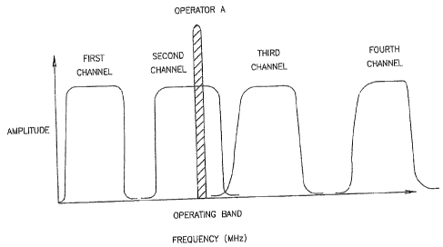
station capacity Turning now to Fig tA, there is shown a spectral diagram
exemplifying frerjuency bands or chamtels (e g 1 ?5 MHz each} of a first
cellular
2
CA 02558849 2006-09-06
operator which may be used within the frequency range of the "l3perating Band"
in a
CDMA channel. Also showr7 in Fig IA is a narrow band interference signal of,
for
example, 35 ICHz bandwidth, introduced by some outside source, within the
frequency
range of a second communication channel of flue Iirst cellular operator. The
interference
signals may reduce the LbII of one or more communication channels, and the use
of a
conventional repeater may serve to boost the interference signal and reduce
the Ebll of
the communication channel with which it is interfering Repeaters, as part of a
t.'.ellular
network system are typically installed geographically far from base station
coverage The
interference may appear in the vicinity of the repeater receiver horizon or in
the vicinity
of the base station receiver horiaon, and may create a problem $'om the
horizon io the
base station receiver Repeaters andlor base stations are not generally capable
of solving
these problems
[4O5) Fig 1B shows a spectral diagram exemplifying possible cha5tnal frequency
hands
that n second cellular operator may use in the same geographic location as the
first
cellular operator of Fig lA 1-lowever, the second operator of Fig. 1B may use
communication charurels with a narrower bandwidth (e g. l00 ICIIz) than those
used by
the first operator in Fig tA, and may also use two or more communication
cltarutels
having adjacent frequency bands, to create the required tragic capability. For
example,
one channel may be primarily used for traffic and the other channels may be
primarily
used for access. All channels may generally need to be operational, so that
the
communication rnay be adequately performed This scenario may typically occur
in
broader areas, a g., between states, countries, or in areas close to water
such as lanes and
seas Base stations that ate installed near a water source may receive an
undesired signal
from far base stations or even from far counhies because water is an excellent
conducer
3
CA 02558849 2006-09-06
of lu' waves Accordingly, as stmwn in Fig, 1 A, the frequency bands of the
operator 13,
e.g , the third channel in Fig. 1B, may overlap and interfere with the
frequency bands of
operator A, e.g, with the second channel in Fig 1A. Additionally or
altemativefy, as
shown in Fig. t B, Ehe frequency hands of the operator A, a g., the fourth
channel in Fig
1A, may overlap and interfere with the fr~edueney bands of operator B, a g_,
witty the sixth
channel in Fig. 1B
[t7(7G] Another exemplary scenario of communication without using a repeater
may occur
in the context of an outdoor environment In tile outdoor environment there may
be
interfetences in the operating base station receiver, a g , interference
signals such as TV
stations or other cellular operators These interferences may affect the base
station, for'
example resulting in cell sluinlrage and/or lower base station capacity. When
a
cvntmunication channel having an interference signal, e.g , as shown in Fig 1
A or in Fig..
I B, is received by a cellular base-station, the interference signal may have
an adverse
effect on the base station receiver. Zither the receiver may not be able to
extract data
from the charmer, or in same cases, the receiver may fully biaclc the receiver
capaciEy or
control charulel.
[007J An interference signal may be of a fixed nature, having relatively fixed
frequencies
and amplitudes Alternatively, an interference signal may be intermittent and
of an
unstable nature.
[008] As sltould be clear from rigs lA and 1B, the center frequencies and
frequency-
band-size of communication channels used by one or more wireless service
aperators/providers in a given geographic location, may vary substantially,
and thus each
channel may have considerably different filtering requiternents when passing
tturough a
repeater andlot at the input stage of a base-station
4
CA 02558849 2006-09-06
SUMMARY OT TFIU IN'VIaNTION
[Ot39j A system and method are provided for enabling digital f ltering of
communication
channels, including adjusting the channels center frequencies. The system and
method
may enable, for example, isolating frequencies associated with individual
aouununication
chatmels and/or groups of communication channels, and in some cases to
extracting or
excluding frequencies associated with narrow band noise, or interfererine from
a
communication channel Given the dynamic nahtre of noise and the possibility
that a
communication channel's center fY~equency may dt ift, of that a communication
channel's
band-size or bandwidth may either expand or shrink, the system and method may
enable,
for example, adjusting the chantreis center frequencies
L(10I0] Some embodiments of the present invention relate to digital filtering
of one or
more communication channels to facilitate the operation of a repeater, by
fiilering
communication signals received at the base-station, and/or by excluding narrow
band
noise/interference either at a base-station or at a repeater
[001 I ] Some embodiments of the present invention relate to a t~eceiver that
may receive a
signal associated with a certain communication chatmet at a specific
frequency. An
analog to digital converter mny generate a digital signal correlated to the
received signoi
and the digital signal may be passed tlVOUgh a digital filter, configured to
filter the digital
signal and pass frequency components at or around Ilse frequency of the
communication
channel's specific frequency A digital to analog converter may generate an
anatog
signal correlated to the filtered digital signal. In some embodiments of the
present
invention, the analog signal may be passed or inputted directly or indirectly
into a base
5
CA 02558849 2006-09-06
station receiver. In other embodiments of the present invention, a transmitter
may
rEtransmit the analog signal eiUter to a base station, a handset of to a
repeater
[0012] According to some embodirtrents of the present invention, there may be
included
a second digital filter configured to pass frequency components, at, or around
a second
frequency associated with a second communication cltannel_
[0013] According to some embodirnents of the present invention, there may be
included
a down-converter to down-convert a received signal to an intermediate
frequency signal
Alternatively, the down converter may down convert the received signal to a
desired
radio frequency signal Additionally or alternatively, art up~converter may be
included to
up~convett tv a transmission frequency an analog signal correlated to the
filtered digital
signal.
[0014) According to some further embodiments of the present invention, a
digital ftlter
may be configured to filter out an interference signal. The digital filter may
either be a
notch filter or a combination of twv filters having partially overlapping band
pass
characteristics
[0015] According to some further embodiments of the present invention, a
control unit
may ptogtarn the first and/or second digital filters according to digital
filter parameters
and/or coefficients, stored in a filter parameter database 1'he controller may
also receive
digital filter parameters and/or coefiicienis from a remote IOCatIon through a
modem.
[001 GJ The controE unit may receive signals from one or mare perFormance
monitors of a
system according to present invention indicating performance parameters, such
as signal
delay, phase shift, gain, and presence of noise/interFerence fu response to
the
perforntance monitor signals, the controller may adjust or change the digital
fslter
6
CA 02558849 2006-09-06
parameters and/or coefficients of one or more digital filter in order to bring
system
performance within operational requirements
[0017] According to some finthet embodiments of the present invention, the
digital
signal, either before or after filtering, may be mixed with a digital
sinusoidal signal at a
shifted fxequerrcy rshift. The shifted frequency may be set and adjusted by
the controller,
either in response to performance monitor signals at based on instmctions
received
tluough a modem
[0018) According to some further embodiments of the present invention, an
analog
signs! produced by the digital to analog converter may be provided to the
input of a base
station receiver
[0019] According to some further embodiments of the present invention, one or
more of
the filter elements may include a time domain to frequency domain conversion
engine, a
frame shaping unit, and a iuequency domain to time domain conversion engine
The
frequency domain conversion engine and the mekhod to operate the engine may
provide
capabilities to monitoring the communication channel traffc and may enable to
detect
interferences characteristics The data on the existing interference and its
characteristic
tnay give a tool, for example, to a customer, to decide if tire communication
channel is
damageable from the interference
BRLJ'uT DTSCItIfTION OT TI3T<; DRAWINGS
[00?OJ The subject mattor regarded as tJre invention is particularly pointed
out and
distinctly claimed in the concluding portion of fhe specification The
invention, however,
both as to organization and method of operation, together with objects,
features, and
7
CA 02558849 2006-09-06
advantages thereof, may best be understood by reference to the following
detailed
description when read with the accompanying drawings in which:
[00? 1 ) Fig I A is n spectral diagram showing four tnvlti-frequency signals
of four,
respective, communication channels, which may be used by s cellular operator
in a
specific geographic region, where the second communication channel is conupied
by an
interference signal;
[003?] Fig IB is a spectral diagram showing five tnulti-frequency signals of
five,
respective, communication channels, which may be used by a second wireless
service
provider/operator in a specific geographic region, where the convnunication
channels are
of a smaller bandwidth than those of Fig. lA and wherein two pairs of channels
are
adjacent to one another;
[0033] Fig 3A is a block diagram showing an example of a bi-directional
repeater
with digital filters and digital frequency shifters according to some
embodiments of the
present invention;
[002~1j Fig ?B is a block diagram showing a<t example of a bi-directional
repeater
with digital filters, n control unit, a perfonnance monitor, and a modem
according to
some embodiments of the present invention;
[0025] Pig 3 is a block diagram showing one possible embodirneni of the
digital
filters and Frequency shifters block of Fig 3A;
[0026] Figs. 4A to 4C are specttal diagrams showing examples of frequency
responses of
digital filters i 440A through 140417 in Fig.3;
[0037] Fig 4L~ is a spectral diagram showing an example of a frequency datnain
representation of n digital sinusoidal signal at a shifted frequency;
s
CA 02558849 2006-09-06
(0028] I=igs_ ~FE and ~r are spechal diagrams showing examples of frequency
shifted
communication channels;
(0029) Pig SA shows a block diagram of a multiple-channel digits! filtering
confrguratian or block according to some embodiments of the present invention;
[OD30j Pig. SB is a series of spectral diagrams illustrtrting exemplary
effects on a signal
by elements in the uptinlt path of the multiple-channel digital filtering
block of Fig. 5A;
(OD31 ] Fig.. SC is a series of spectral diagrams illustrating exemplary
effects an a signal
by elements in the downlink path of the multiple-path digits! filtering
configuration of
rig. 5A;
[D03?J Fig, 6A is a block diagram of an alternative digital littering
configirr~rtton or block
i~0 incorporating a Past Fourier Transform {"FF'T"), progranvnable frame
shaping, and
sn Inverse Fast Pourier Transform {"IFFT"), accot~ling to some embodiments of
the
present invention;
(0033] Fig. 613 is a series of time domain and spectral diagrams illustrating
exemplary
effects on a signal by each element in the digital filtering block of Fig 6A.
(OD34j Fig 7 is a block diagram showing another example of a bi-directional
repeater
with digital fillets and digital frequency shifters according to same
embodiments of the
present invention, where digital filter and frequency shifting parameters may
be adjusted
and/or regulated;
[0035] Fig_ 8 is a block diagram showing a communication channel with digital
f ltering
system and or frequency shifting, which may be combined, far example, with s
Tower
Mounted Amptifeer (TMA) or Tower Top Amplifier (TfA) in front of a base
station
front end according to some embodiments of the presetrt invention confgured to
operate
in conjunction with a base station; and
9
CA 02558849 2006-09-06
[0(336) Pig. 9 is a flow chart describing a method of implementing digital
filtering,
according to some embodiments of the presetrt invention.
[0037] tt wilt be appreciated thai for simplicity and clarity of illustration,
elements
shown in the figures have not necessarily been drawn to scats. Por example,
the
dimensions of some of the elements may be exaggerated relative to other
elements For
clarity. Further, where considered appropriate, reference numerals may be
repeated
among the figures to indicate corresponding or analogous elements
10
CA 02558849 2006-09-06
n~cx~l_,~cn nl;sc~rr>orr
[0038) In the following detailed description, numerous specific details are
set forth in
order to provide a thorough understanding of the invention. however, it will
be
understood by those slcilIed in the art that the present invention may be
practiced without
these specific details, In other instances, well~ln~own methods, procedures,
components
and circuits have not been described in detail so as not to obscure the
present invention.
[0039] Unless specifically stated otherwise, as apparent from the following
discussions,
it is appreciated that tluoughout the specification discussions utilizing
terms such as
"processing", "computing", "calculating", "determining", or the like, refer to
the action
andlor processes of a computer or computing system, or similar electronic
computing
device, that manipulate and/or transform data represented as physical, such as
electronic
quantities within the computing system's registers and/or memories into other
data,
similarly represented as physical quantities wiWin rife computing system's
memories,
registers or other sueir infomyation storage, transmission or display
devices..
[OO~tOj Embodiments of the present invention may include apparatrtses for
performing
tlae operations herein. Such apparatuses may be specially constructed for' the
desired
purposes, ar they may be implemented using a general purpose computer
selectively
activated or reconfigured by a computer prograun scored in the computer Such a
computer program may be stored in a computer readable storage medium, such as,
but is
not limited to, any type of disk including filoppy disks, optical disks, CD-
lZOMs,
magnetic-optical disks, read-only memories (IiOMs), random access memories
(ItAMs},
eiectricaAy programmable read~only memories (EPItl7Ms), electrically erasable
and
pragrammabte read only memories (EEPRQMs), magnetic or optical cards, or any
other
CA 02558849 2006-09-06
type of media suitable for storing electronic instructions, and capable of
being coupled to
a computer system bus
[0041) The processes and displays presented herein are not inherently related
to any
particular computer or other apparatus. Various genernl purpose systems may be
used
with programs in accordance with the teachings herein, or it may prove
convenient to
constnrct a more specialized apparahrs io perform the desired method The
desired
structure for n variety of these systems wilt appear from the description
below In
addition, embodiments of t)se present invention are not described with
reference to any
particular pragrammmg language It will be appreciated that a variety of
programming
languages may be used to implement the teachings of the inventions as
described herein.
[004?J Turning now to fig. 2A, t)tere is shown a block diagram of a bi-
directional
repeater 100 with a digital filters and digital frequency shifters block 140U
according to
some embodiments of the present invention The bi-directional repeater ) 00 may
include
two basic sections: (A) an upstream or up-linlt section which receives signals
from a
mobile devise (e g. cell phone) and retransmits the signal to a base-station;
and (B) a
downstream or down-iir~lt section whiclr receives signals from either a base-
station or an
upstream repeater, and retransmits the signets to a mobile device or to a
downstream
repeater-
[0043) T~ooking first at the up-link section (A) fianr left to right in I~ig_
2A, there stay be
an input filter 110U, which for this example, may be a radio frequency
("IZ.F") filter, of
more specifically, may be a fitter tuned to pass frequencies in the range of
an Operating
Band, a g_, 800 to 830 MHz The input 1tF filter 11011 may receive signals from
an
antenna and may pass frequencies in the frequency range of one ar more
cornrnunicntion
charurels to be repeated to a down converter 120U The down converter 120U may
mix a
12
CA 02558849 2006-09-06
received signal with a sine of cosine signal of a given frequency such that
the received
signal may be down-converted to an intermediate frequency ("iF") signal.
Alternatively,
the received signal may be down converted directly to the desired 12F signal
Eidter or
both of the input 1ZT filter i l0U and tire down converter I~QU may include a
signal
amplifier (not shaven in Fig ?) An analog to digital ("AID") converter 130U
may
sample, e.g., at the rate of GOM SatnpleslSec, tire IF signal and tnay
generate a digital
signal representing the sampled IF signal The digital signal representing the
IF signal
may enter digital filter and frequency shifter block 14DU.
[0044) Tunring now to Fig. 3, there is shown a bioclc diagram of an exemplary
embodiment of a digital filfier and Frequency shifter bloclt i40U, including,
for example,
digital frlters 1400A to I400D, mixers 14GA and 146B, and digital sintrsoidai
generators
144A and 14413 The frequency slrifter implemented in the digital filter and
frequency
shifrer block 1r10U may be digital. A digital signal entering block 140U may
be filtered
by eaclr of a plurality of digital filters 1 d00A tluough 1400D and tire
output of each of
the digitol filters may be combined by an adder I42 or by a f~tnctianally
equivalent
device Each of tire fitters witlrin tire digital filter 140U may have a
separate and distinct,
a g., independently defined, frequency response. Digital filters I4DU mrd/or
140D may
include any number of digital filters and/or combination of ftlters, and the
four digital
filters 1400A Lo 1400D in Fig 3 are described only as an example.
[OD45) Digital filters are well lcnawn in the field of con urtunicatians
Implementation of
a digital filter bank may be performed using a single processor or multiple
processors,
a g , a digital signal processor ("DSP"), or may be implemented on a single or
multiple
dedicated digital filtering circuits, e.g., field programmable digital filters
In the example
of Fig 3, there are spawn rive discrete digital filter circuits As part of
some
73
CA 02558849 2006-09-06
r
embodiments of the present invention, digital filters I400A through 1400D may
be field
programma6)e digital filters ("rPAF"} Tlrat is, each filter's transfer
function, along with
its frequency response, may be programmed, reprogrammed or adjusted, as
required
[0046] Turning now to Figs. 4A through 4C, there are shown exernples of
possible
frequency responses for digital filters 1400A though 1400D of Fig. 3, where
digiial
filters 1400A through 1400D may con-espand to the first tluough the fourth
communication chanJtels exemplified in hig. lA, respectively That is, the
impulse
response or frequency transfer characteristic for each digital filter 1400A
tlvough 1400D
may be separately set or adjusted to pass frequency components of digital
signals that are
at or around the carrier/center frequency of the filter's corresponding
communication
channel For example, digital filter 1400A may be programmed with a transfer
function
having a band pass frequency response peaking at or around tire cariier
fredueney of the
first conuiwnication channel shown in Fig. 1 A Digital filter 14000 may be
programmed
with a transfer function having a band pass frequency response peaking at or
around the
carrierlcenter frequency of the third communication channel shown in rig 1 B,
and may
have a bandwidth smaller than that of filter 1400A, since the channels sltown
in Fig. 1B
are narrower than those shown in Fig. 1 A
[0047] Digital filters 1400B~ and 14()OI33 of Fig. 3 may be arranged in series
and each
may be programmed to have a partially overlapping band-pass frequency response
with
the other, as shown in Fig 4B An applicailan of the resulting frequency
response of the
combined filters may be the exclusion of interference signals such as the one
shown in
the second charme! of operator A in rig 1 A If an interference signal is
present within a
commw~ication channel's frequency band, the filters may be configured to
produce a
frequency response having two sub-bands or a notch or stop band, at or around
tl~e
14
CA 02558849 2006-09-06
i
frequency of tire interference signal For example, as shown in Fig lA, a
cotnmunication channel (second communication channel) may have ftr'quency
components between, for example 824Mhz and 849Mhz (known as the cellular
s
frequency band), and an interference signal, a g , a television signal from a
neighboring
country, may have a frequency band of; for example, 839Mhz to 84t)M)tz. the
filters
I~400Bt and I~OU$3 ratty be configured to produce a frequency response to pass
most of
the frequency components between the cellular frequency band and to exclude ar
suppress frequency components between, for example, B39Mhz to B~OMhz, thereby
stopping the interference signal from propagating tlrrouglt Ehe digital filter
I~IOU and
being repeated or retrrrrtsnutted l~lumerous filter designs, e.g , a notch
filter, a stop band
f lter, a two sub-bands f Iter, or arty other suitable filter and/or
combination of filters may
be used to produce a selected frequency response. For example, the selected
freeyuency
response may have the property of passing most of the frequency components of
a
contmunicatian chmtnel, attd suppressing, ar excluding frequency components of
an
interference signal within the frequency band of the communication channel
llnts, the
frequency response to an interference signal may be based an a predetermined,
a g ,
anticipated interference pattern, such as but not limited to a television
signal from a
neighboring country, ar in response to an actual received interference signal,
e.g~, a
temporary random signal, wltich may nor be known in advance
[0018] the physical design of digital filters having desired ttnnsfer
functions is well
known in the art. Although specifte filters and transfer functions are
mentioned above,
any digital filter and transfer function combination, currently Imown or to be
devised in
the future, may be used as part of the present invention Fw~tltemiore, ttte
digital filter ar
Flters may include ASIC's and I~PCA's and/or a I7SP engine wltich are well
Itnown in
CA 02558849 2006-09-06
the art, arid which rnay be reprogra~tmied in response to a shift in the
frequency
composition of an inteoerence signal That is, if the frequency band of the
intet~'erence
signal changes, the digital filter or filters may he reprogtauttned, manually
at
autamatieally, to shift the notch or stop band region to correspond with the
interference
signal's frequency band. Notch filters performance may be changed to optimize
the
chartneJ performance. Such optimisation of the channel performance may be
achieved,
for example, by reprogramming andlor modifying various parameters, a g , the
Blter
bandwidth, attenuation, delay, by modifying the filter slops, or by providing
linear phase,
and minimum in/out band delay variation etc
[0049] Also sltown in Fig 3 are three digital frequency-shifting units. Tlte
first
frequency-shifting unit ntay include, for example, a digital sinusoidal signal
generator
144A to produce a digital sinusoidal signal, e.g,., a numerical control
oscillator, at a
shifted frequency F,s,~n~, and a digital ntfxer 14GA to ntix the digital
sinusoidal signal with
an output of a digital fitter, a g, digital filter t.f00D. The second
frequency sltifter unit
may include a digital sinusoidal signs! generator 144B to produce a digital
sinusoidal
signal at a shifted frequency 1'si,EnZ, and a digital mixer 1468 to mix the
digital sinusoidal
signal with the output of digital signal adder 14?. The third frequency
shifter unit may
include a digits! sinusoids) signal generator 1440 io produce a digital
sinusoidal signal at
a shifted frequency F~~,~ns, and a digital mixer i46C io mix the digital
sinusoidal signal
with an input io a digital filter, e.g , 14000 Signal shifting units may shift
the frequency
of the signals to which tltey are applied by the frequency of the digital
sinusoids( signal
produced by their respective digital sinusoidal generators.. Zi;g. dD shows a
spectral
diagrarn of a digital sinusoidal signal, which digital sinusoidal signal
appears as an
impulse at the frequency of the signal (Fsi,tn) 1~ig~ 41; shows a spectral
diagram depicting
is
CA 02558849 2006-09-06
a shift in the Frequency components of a single communication channel, as rnay
resv)t
flout Ute application of a frequency shifter to the either the input or output
of a digital
filter 140 Fig, 4TH shows a spectral diagram depicting a shift in tire
frequency
components of several communication channels, as may result from the
application of a
digital frequency shifter to the output of digital signal adder 1 ~1~
[0050) Generally, mixing a digital signal with a digital sinusoidal signs! may
result in
shifting of the frequency components of the digital signal by the frequency of
the
sinusoidal signal The shift may be both up and down in frequency, and
harmonics may
also be ptadvced by tire process. Thus fJtets may be used to isolate the
desired
fiequency band Digits! ftltets may be used to remove harntonics front the
output of
miters 146A and 146A, if desired
[0051] Now turning back to Fig. 2A, there is shown, directly after the digiia)
flier and
frequency shifter block i 40t1, a digital to analog converter ("D/A") 150U The
D/A 1 SOU
may convert the digital signal output of the bioek 140U to an analog signal,
which may
then be up-converted by up,converter I60U to the original frequency received
at input
RF filter 110U An ouiput filter I70U may be used to remove harmonics thaE may
have
been introduced into the signal by the up-converter 160U. Either or both of
the up-
converter 160U and the output RF' filter i 70U may include a signal amplifier
(not sltown
in Pig ?A) Tlte filtered signet may then propagate to and ovt of a
transmission antenna
[0052] The downstream or down-link (B) section of the bi-directional repeater
I00 may
substantially mirror the up-stream section (A) discussed above One difference
may be
that the ittpttt 1tF filter 11 OD, digital filters and digital frequency
shiner block 140D arid
output RP filter 170D may be tuned to receive and pass frequencies of
downstream
17
CA 02558849 2006-09-06
communication channels, as opposed to passing frequencies at or around
upstream
communication chameis_
[0053] the specific frequency bands to which each of the filters is set may
depend on the
specife fiequencies of the communication channels, upstream and downstream,
tlret an
operator may wish to repeat within a specific geographic location. The
frequencies
shown in rigs. lA and ID are only examples of such communication cltannel
fiequencies No distinction is made between upstream arid downstream channels
in Fig.
3A. However, it will be understood by one of ordinary skill in the art that in
a cellular
system, or any other two-way wireless communication system, there may be a
corresponding upstream communication channel far each downstream
conrrnutrieation
channel. The relation between an upstream channel frequency and a downsircarn
charmel frequency may be fixed, ar each may be negotiated or set separately
between a
mobile device and a base station
(005~tJ Fuming now Eo Fig. 2B, there is shown a block diagram of an
embvdirrtent of tire
present invention including a control unit 300 connected to digital filters
1~OU and 140D
and receiving performance data from a performance monitor 180 The control unit
?00
may program and/or adjust configurations, parameters, and consequently
filtering
characteristics, of each of the digital f Iters 1400A to 1400D (shown in fig..
3) within
either of the digital filters IOU and IdOD The control unit ?00 nay program or
adjust
each digital filter 1400A, I~OOB, 1~IOOt~, or 1400D based on parameters stored
in
parameter databases ~ 1 OA and 210B, based on instructions received remotely
(e g , via
modem or otlrer external source), or in response to performance signals
received from n
per farmance monitor I 80
1$
CA 02558849 2006-09-06
[DOSS] According to some embodiments of the present invention, the control
unit 200
may program ar adjust the parameters andlor digital filter coef$cients of a
specific digital
filter 1400A, 14DOB 14DOC:, or 140DD, or digital filters 140U and 140D,
collectively, in
order to accommodate operational or performance requirements associated with a
specitc conunuuication channel or set ofi communication channels For example,
the
control unit ?00 may program one of the digital filters 140DA-I4DOI)
corresponding to
the frequency band of the first communication channel in Fig. IA. Thus, the
control unit
200 may produce or generate a digital filter 1400A, 1400B, 1400r, or i400D
with a
digital filer configuration and coefficients resulting in band pass frequency
response
characteristics consistent with the center frequency and bandwidth of the
first
comnttnticatian channel in Fig- IA The contra! unit 300 may program or adjust
a
second digital filer with a confguration arid coefficients to produce a second
digital
filter 140DA, 14DOH, 14000, or I~100D having hand pass frequency response
characteristics consistent with the center frequency and bandwidtlt of the
second
cammtutieation clrartnel in Fig. I A, and having a notch in the band pass
region
[DOSG] Likewise, v~itlsin the same digital filters, 140U or I~IDD, as within
the first and
second digital filters mentioned directly above, the control unit 200 may
program a third
digital filter to ftltet either a single narrowband communication channel, a g
, t3re ftfth
channel shown in Fig IB, or a set of adjacent uatrowbattd channels, e.g, the
third and
fourth communication channels shown in Fig. 1B Each digital filter 1400A-1400D
may
ve programmed with a tuvque and independent configtrration and coefficients
and may
have a frequency response completely independent from those of any of other
filters in
either digital filter 140U of 140D.
19
CA 02558849 2006-09-06
[0057] The contznl unit 300 may adjust a filter's configuration andlor
coefficients in
response to signals from the pezformance rnonitor 180 Performance monitor 180
may
monitor pazazneters such as signal delny, phase shift, attd gain across the
one or more
filters and/or one or more other components of a system according to
embodiments of the
present invention For example, if the perforntanee ntonitor indicates to the
controller
that signal delay, phase shift, andlor signal loss across one of the filters
1400A-1400D
exceeds a threshold value, the control unit 300 may adjust or change the
digital filter's
configuration to compensate accordingly In general, complex filter
configurations may
provide more well defined and enhanced filtering parameters than relatively
simpler
configurations; however, SUCH enhanced parameters may be obtained at the
expense of
time delays and phase shifts across the filter. 'therefore, according to some
entbodiments
of the present invention, if control unit ?00 detemtines that a particular
frlter 1400A to
1400D has an excessive delay andlor phase shift, the controller may reprogram
or adjust
that particular filter to a simpler configuration. Such reprogramming may be
implemented ntanually and/or automatically. Although simpler filter
configurations may
produce poorer characteristics, such as smaller, less defined slopes an the
edges of the
filter's band, the delay and/or phase shift values of such configurations may
he improved
significantly Tn another example, the control unit z00 may program digital
f:lter I~OOA,
I400B, 14000, ar 1400D to have a bmtdwidth sufficient to pass frequency
components
of multiple adjacent communications channels, for example, U1e third and
fourth channels
in Fig tB It will be appreciated that in certain operational situations, such
as when two
communication channels are filtered using one digital filter 1400A, 1400B,
14000, or
1400D, it may be beneficial to adapt dre configuration and coefficients of the
digital f lter
so as to have a wider band pass region and/or shorter and less defined slopes
20
CA 02558849 2006-09-06
(0058] It sltould be clear to one of ordinary slcili in the alt that the
control unit 300 may
dynamically utter the configurations and coefficients of any of the filters
1400A-1400D,
based either on data stored in databases 310A and ? I OB, or on data received
from a
remote souroe, for example, viamodem 330, or on a combination of both Database
2,1 OA
may store data related to downlink conversion and database ? 1 OB may score
data related
to upiinlc conversion. For example, the cankoller may receive an instruction
thmugh the
modem 320 to reconfigure the butdwidth of a filter cutrently configured to
pass only one
communication chatutel, to now pass two communication channels The cozttrol
unit 300
may be instructed to reco~gure filters based on data in the databases 310A and
'310B
and/or rnay be provided with the new configuration and coefficients via modem
230
Furthermore, new filter configuration and coefficient data may first be
uploaded to
databases 310A and 310B from a remote source, for example, via modem 220,
following
which conk-o) unit 300 may receive an instruction to reco~gure filter 1400A,
14008,
14000, andlor 1400I~ based on the new data In another embodiment of the
present
invention, petfotmance monitoring data fiom tile performance monitor I80 may
be sent
to control unit X00 via modem 2~0
[0059] Taming now to Fig. 8, there is shaven an embodiment of the present
inveniian
suitable as an input stage to a conventional cellular base station, a
conventional repeater,
or any other conununication system whit a receiver In the embodiment shown in
Fig 8,
there may be a pre-filtering stage 115 which ntay include, for example, a low
noise
amplifier ("LNA") and attenuator A ItF unit 125 may contain a dov,7t converter
and
may down convert the output of the pre--filtering block to an intermediate
frequency
("IF") signal An Alt7 converter (nut shown) may be included in the ItF unit
125 at in a
digital filter block 1400 Tlte down converted signal may be converted into a
digital
21
CA 02558849 2006-09-06
signal by the AID convener, and tire digital signal may be filtered by digital
filters in the
digital filter bloclt 140U as described above (see also up link section A in
Fig. ~A, Fig.. 3
and Figs 4A-rr)
[OO60j One of ordinary skill in the art should understand that down converting
of the
analog signal to an intermediate frequency may not be required if an A/D
converter
having a sufficiently ltigh sampling rate is used. Typically, in order to get
art accurate
digital representation of an analog signal, a sampling rate of twice the
highest frequency
component in the analog signal is required Thus, down converting to an
intermediate
signal may allow for the use of a slower and cheaper A117 converter, however,
it is not
essential
[0061] Once a digital signal representing the received analog signal is
produced, fltering
of interference signals and frequency shifting of conmtunication channels may
be
performed as described above wilt reference to Figs 3 and 4A to 4F The digital
filters
1400A, 14008, 14000, or 1400D, may be configured to produce any one of a
number of
transfer characteristics or frequency responses, including notch faltering of
a natxow band
interference signal.
[006Zj Once filtered, the digital signal may be convened back into an analog
signal using
a I7/A converter (not shown) The output of the F7/A converter may be up
converted, if a
corresponding down conversion step was previously used, e.g., before
digitizing the
signal. The DIA converter ntay either be part of the digital fitters block
140U or part of
the ItF unit 125 The up converter, if used, tnay be prat of the RF unit 125.
[0063] The a~talog output of the above described embodiment of the present
invention
may be supplied to an ItF input stage of a conventional base station, as shown
in Fig. 8,
22
CA 02558849 2006-09-06
or to the input stage of a conventional repeater, or to any otlter receiver
used as part of a
3tF communication system
[OOG4] Turning now to TIg. 5A, there is shown a block diagram of a multiple-
path digita3
filtering configuration of block l~IOU of Fig. 8 according to some embodiments
of tire
present invention. The filtering configuration of Fig SA may have multiple
parallel
signal paths where each signal path may induce multiple littering elements.
The first and
second signal paths may include a digital down converter, a base band digital
Flter, and
digital up converter Reference is made to f~'Ig. SB which shows a series of
spectral
diagtan~s illustrating exemplary effects on an inptrt signal by elements in
the lop path of
the multiple-path digital fiifering block of Fig SA and to Rig. SC, which
shows a series
of spectral diagrams illustrating exernplary effects an an input signal by
elements in the
lower path of the multiple-path digital $ltering block of Fig SA, As shown in
Figs. SB
and SC, a digital down converter may shift downward tare frequency components
of a
digital signal, e.g , by a frequency of a first digital sinusoidal signal
(FoDC) provided by a
first digital sinusoidal source. According to some embodiments of the present
invention,
a digital base-band filter rnay be used to filter the down-converted or down-
shifted digital
signal, and a digital up converter may up-convert or shift up the fi~equerrcy
band of the
output of the digital Ease-band filter by a frequency of, a g , a digital
sinusoidal signal
(ForJC) provided by either the first or second digital sinusoidal source.
[006SJ According to some embodiments of the present invention, each digital
down
converter and each digital up converter may be associated with a separate
digital (e_g.,
sinusoidal) signal source, wherein each of the digital signal sources may be
individually
controlled to provide a separate digital signal of any frequency within the
source's
operating range Each of the base stations band digital filters may be
progtanmred with a
23
CA 02558849 2006-09-06
separate configuration and/or filter coefficients According to some
embodiments of the
present invention, the digital converters, digital up converters, their
associated digital
sources and each digital base band filter may be individually adjusted or
controlled by
canirol unit Z00
[DOGS] Turning now to Fig SA, there is shown a block diagram of an alternative
digital
Fltering block 140 where signal filtering may be accomplished using a Data
Framing unit
1401, a spectTUm analyzer (e g., Fast Foutier Transform ("FFT") engine) 1402,
a
programmable frame shaping unit 1403, and an Inverse Fast Fourier Transform
("IFFT")
engine 1404; and to Fig 613, which shows a series of time domain and spectral
diagrams
illustrating exemplary effects on a signal by each element In the digital
filtering block of
Fig SA.
[0067) According to the exemploiy flteting system of Fig 6A, a sampled data
stream
may be parsed by the Data Framing unit 1401 into individual frames of data The
frames
may or may not partially overlap, and each frame may pass through a Fast
Fourier
Transform engine 140?, or some other time domain to frequency domain
conversion
block Each frame of data output by the rFT engine 140? may pass through a
progrartnnable FFT Frame shaping bloclt 1403 The frame shaping block may be
programmed to suppress or notch out portions of the frame associated with
undesired
frequency components and to not affect or, optionally, to boost elements in
the frame
associated with frequencies of interest The IFFT engine 1404 may be used to
convert a
frequency domain frame, which has passed through the frame shaping unit or
black, back
into a Eime domain frame The frames may then be recombined into a digital data
stream
representing the original data sttr:am in the time domain, but with unwanted
frequency
components removed and with wanted frequency components either untouched or
24
CA 02558849 2006-09-06
enhanced_ According to some embodiments of the present invention, the
programmable
FFT frame shaping unit t403 may be programmed by a control unit ?OD. Removing
unwanted frequency components may be done manually or automatically by the
programmable FFT frame shaping unit in accordance witlt the insiruclions
programmed
into control unit 30D In addition, control unit ?00 may include a modem that
may enable
remote access to remotely remove unwanted frequency components, or to remotely
program control trait ?00
[0068] In contrast with the digital filtering configurations or b)ocks spawn
in Figs. 3 and
SA, the filtering conf guration of rig 6A may allow for the filtering of a
large number of
non-adjacent communication channels, a s., of varying bandwidths attd center
frequencies, to be performed using, for example, tluee processing elements;
namely, the
FFT engine 140?, the programmable FFT frame shaping unit 1403, and the IFFT
engine
1104 A fitrther distinction between the two filtering methodologies Lies in
the fact that
conventional digital filters operate purely in the time domain, white the
filtering block o~
Fig 6A converts a digital time domain signal into the frequency domain before
stripping
out or nul)ifying valves corresponding to unwanted frequency componettts Since
the
processes of converting a digital time domain signal into a frequency domain
signal are
generally con tputationally intense, and may thus introduce long delays, such
processes
have not been previously considered for real-Eime digital signal filtering.
Such processes
may be useful artd worthwhile in the context of the present invention, a g, in
order to
detect artdlor identify recurring interference pattetms off line, sa that such
anticipated
patterns may be subsequently taken into account as described above The history
of
anticipated patterns that are detected andlor identified may be logged or
stored in
memory for later reference
25
CA 02558849 2006-09-06
[0069] In accordance with some embodiments of the present invention the
frequency
domain conversion engine and the method to operate the engine rnay provide
capabilities
to monitoring the cotmnunication charurel traffic and may enable to detect
interferences
characteristics. The data on the existing interference mid its characteristic
may provide an
end user, far example a customer, with a tool to decide if the communication
clrannel is
danrageable from the interference
(0070) Turning now to F'ig. 7, thet~e is shown another possible embodiment of
a bi-
directional repeater 100 according io the present invention As in the bi-
directional
repeaters of Figs ?A and ?B, tireee are two sections; (A) an upstream or up-
link section,
and (B) a downstream or down-link section Also, as in the embodiment of rig.
2, the
up-fink and down-Link sections may substantially mirror one another except far
the
frequencies they are tuned to pass and retransmit.
(0071 J Looking at the downstream or down-link section (B) of the bi-
directional repeater
100 of Pig 7, ti~ere may be a duplexer including rut input RF filter 1 IOD.
The input RF
Flter 110D may lead to a pre-filtering stage 115D which may include a low
noise
amplifier ("LNA") and an attenuator. The output of the pre-filtering block
115D may
enter an ttlr unit 125D which may down convert the output and may also include
an AID
convener. Digital Filters and digital frequency shifters in a digital block
140D may be
similar to the ones described for Figs ?A, 2B, 3 ar 4A Ylrrough SIC, or may
include any
other digital filters and digital frequency shifters suitable for the present
invention The
output of the digital filter block MOD may enter the 1tF trait 1?SD, which may
up
convent the output and may also include a DIA converter A power amplifier
block J~15D
may include, for example, an attenuator, a high-power amplifier, end n power
monitor.
An automatic gain control circuit ("AGC") may adjust the attenuator such that
the output
26
CA 02558849 2006-09-06
signal from the power atnpliFter black 145D remains substantially steady AGC
may
enable automated gain setting, automated gain balancing and/or automated
oscillation
protection the output signal of the power amplifier 6loctt 145D may propagate
to and
through a duplexes including an output filter 170D
[0077] As far the bi-directional repeater 100 in Figs 2A and 2B, the bi-
directional
repeater l00 of Pig. 7 may be configured to repeat specific sets of
cornrrrunication
channels, at or around specific carrierlcenter frequencies, in the upstream
direction,
andlor to repeat specific sets of communication channels, at or around
specific carrier
frequencies, in the downstream direction. Digifal fillets and digital
Frequency slufters in
the digital blocks 140tJ and 140D, may be adjusted to pass only frequencies at
or around
the carrier frequencies of the relevant connntnrication channels Frequency
components
of one or more commwication channels may be shifted using a digital frequency
shifler.
Carrier frequency offsets due to up~couversion or down-conversion may be taken
into
account and compensated for within the digital filters. Furthermore, the bi-
directional
repeaE~er I00 of the present invention may be adjusted to notch out narrow
band noise
interference(s) within the communication channels' frequency band .
[0073] Also shown in Fig. 7 is a performance monitor Ii#0 connected to various
points
along the upstream and downstream signal paths. Monitor 1$0 may be used to
traclt
characteristics such as gain, time delay and phase across various elements of
the repeater
i00, including individual digital fitters Monitor Ig0 may transmit signals
indicative of
the monitored characteristics to a controller 200, which may make adjushnents
to various
elements of repeater 100, including individual digital filters and frequency
shifters 140U,
in response to the monitor signal Gantraller 200 may matte changes to filter
configuration and coefficients based on data stored in databases 210A and 210$
and
27
CA 02558849 2006-09-06
instruction or data received tluough modem 220. Performance monitoring data
may be
transmitted to a remote location via modem Z~0
[007r1J One of ordinary skill in the art should understand that the described
invention
may be used for various types of wireless or wire communication systems,
including but
not limited to a Tower Mounted Amplifier, wireless, wire, cable or fiber
servers, e.g,
where a narrow interference lies to be filtered out, and/or where phase
linearity and ftltet
parameters leave to be software progranunable, andlor when the interference
may occur
in the conununication channel
[0075] According to some embodiments of the present invention, methods are
provided
for signal filtering As can be seer with reference to rig. 9, at block 90 a
received signal
may be sampled arid a data stream con-esponding to the received signal in the
time
domain may be produced. At block 9i the stream may be filtered in accordance
with one
or more sets of frequency bands associated with one or more, respective,
communication
channels At bloctc 9? one or more communication channels may be co~gured based
on
one or more selected parameters. The metltod may further include, at block 93,
down
converting the received sigrtal to an intermediate frequency prior to the
sampling by tire
analog to digital converter, andlor, at block 94, up converting an output from
tire digital
to analog converter into an output radio frequency filter. At block 95 the
method may
include converting an output of the filtering btoctc into an analog signal In
some
embodiments the filtering may include, at hloelc 96, converting the data
stream from the
trine domain to a frequency domain; shaping a frame of the data stream; and
converting
the data stream back from the frequency domain to ilte tune domain.
[0076] In additional embodiments the signal filtering method may include
monitoring
signal flow characteristics; indicating the signal flow cltaracteristics to
the controller; and
28
CA 02558849 2006-09-06
reconfiguring one or more filtering elements if the signal flow
characteristics are not
within predefined ranges In some embodiments the monitoring of the signal flaw
characteristics may include gaining a signal; delaying the signal; and
shifting a phase of
the signal In soma examples the monitoring includes transmitting the signal
flow
characteristics to a remote location via a modem
[0077] In ftn then embodiments the signal filtering method may include
implementing
automatic gain setting, implementing automatic gain baJaucing, andlot
implementing
oscillation control. In outer embodiments the method may include analyzing a
traffic
load..
[0078] While certain features of the invention have been illustrated and
described herein,
marry modifications, substitutions, changes, and eduivalents will now occur to
those
skilled in the art It is, therefore, to be understood titat the appended
claims are intended
to cover all such modifications and changes as fall within the true spirit of
the invention
29