Note: Descriptions are shown in the official language in which they were submitted.
CA 02559168 2008-07-24
Illuminating Mechanisrn For A Lock
Field of the Invention
The present invention is directed to an iniproved combination lock, and more
specifically to a combination lock which includes a means for illuminating a
portion of the
combination dial.
Background
Security devices, such as locks, are used in a variety of applications to
secure a
variety of objects. In some instances the security device may be used in areas
of low light,
which may impede or complicate operation of the security device. For example,
operation of
a combination dial to locate the correct number of the unlocking combination
or locating the
keyhole for insertion of the appropriate key may be difficult in areas of low
light. As such, it
is desirable to provide a security device that produces sufficient light to
allow easy operation
of the security device.
Summary of the Invention
A lock including an illuminating device which is actuated by the rotation of a
lock
dial to produce an illumination event is disclosed. The illumination event
provides sufficient
light on the lock such as to allow easier operation of the lock in areas of
inadequate light. In
some embodiments, the lock may include a piezo device which creates electrical
current to
light one or more light emitting diodes for a predetermined duration of time.
Brief Description of the Drawings
In the accompanying drawings, which are incorporated in and constitute a part
of this
specification, embodiments of the invention are illustrated, which, together
with a general
description of the invention given above, and the detailed description given
below serve to
illustrate the principles of this invention.
1
CA 02559168 2006-09-08
WO 2005/088038 PCT/US2005/008132
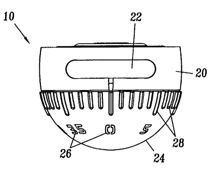
Fig 1 is a top view of an illustrative embodiment of a lock incorporating an
illuminating mechanism.
Fig. 2 is a front view of the lock shown in Fig. 1.
Fig. 3 is a bottom view of the lock shown in Fig. 1.
Fig. 4 is a side view of the lock shown in Fig. 1.
Fig. 5 is a front perspective view of the lock shown in Fig. 1.
Fig. 6 is a back perspective view of the lock shown in Fig. 1.
Fig. 7 is a front exploded view of the lock shown in Fig. 1.
Fig. 8 is a rear exploded view of the lock shown in Fig. 1.
Fig. 9 is an example of a circuit for an illuminating mechanism.
Fig. 10 is a second example of a circuit for an illuminating mechanism.
Fig. 11 is a third example of a circuit for an illuminating mechanism.
Description of the Invention
Figures 1-6 illustrate one embodiment of a lock incorporating a illuminating
mechanism for improved operability in areas of low light. The illuminating
mechanism is
housed within the lock body and when activated, provides light that allows the
user to view
the lock with sufficient light to allow for operation of the lock. In the
embodiment shown in
Figures 1-6, light emits from areas, such as, for example, the numbers or
number markers.
Additionally, light may also emit through other features, such as a logo, the
edges of the dial,
or patterns formed in the dial, or any combination thereof. The light source
can be used to
improve operability of the lock in areas of low light and/or may provide an
enhanced
aesthetic appearance. It should be appreciated that Figures 1-4 illustrate
only one exemplary
embodiment of the present invention and that other embodiments incorporating
the features
disclosed herein are also contemplated. While the illustrative example is
directed to a
specific combination padlock, the features of the present invention could be
applied to many
other products, such as other combination locks, door locks, locker locks,
padlocks or keyed
locks.
2
CA 02559168 2006-09-08
WO 2005/088038 PCT/US2005/008132
The lock 10 shown in Figures 1-6 includes the standard features of a
combination
lock, namely a lock body 20, a shackle 22, and a combination dial 24. The
combination dial
24 includes numbers 26 and number markers 28, although other combination lock
dial
features may also be used. The combination lock 10 shown in Figures 1-6 may
use any
conventional locking mechanism.
Figures 7 and 8, illustrates an exploded view of the lock 10 shown in Figures
1-6.
The lock 10 shown in Figures 7 and 8 includes dial base 301ocated between the
lock body 20
and the dial 24. Also illustrated is one embodiment of the illuminating
mechanism. Included
are a piezo device 33, a piezo wiper 35 having three piezo wiper springs 37, a
print circuit
board (PCB) 40, and a power source 42. The power source 42 is shown as several
small coin
cell lithium batteries, however it should be appreciated by one skilled in the
art that any
power source could be used. For example the power source may be batteries,
fuel cells, solar
power, or the like and will define the performance and several other
properties or product
characteristics of the lock and illuminating mechanism
As shown in Figures 7 and 8, the illuminating mechanism is disposed within the
lock
dial 24 and thereby provides an area for the illuminating mechanism that is
away from the
locking mechanism. This allows the illuminating mechanism to be accessed
without granting
access to the locking mechanism, which would potentially compromise the
integrity of the
lock. Furthermore, while the dial 24 is shown as a hollow semi-spherical
shape, it should be
appreciated that other embodiments can incorporate other types or
configurations of the lock
dial. The hollow, semi-spherical dial allows for ease of incorporation of the
illuminating
mechanism.
The piezo wiper 35 is shown as a stamped metal disk with three wiper springs
37 and
a tab 43 to engage a fixed point 44 in the lock body 20. Although three wiper
springs 37 are
shown, it should be appreciated that only a single wiper spring 37 is needed.
It should be
appreciated that any number of piezo wiper springs 37 can be used, however
three piezo
wiper springs are preferred in order to trigger the light on with one third of
a dial rotation and
to provide a balanced three point surface to support the dial base 30 evenly.
Furthermore, the
piezo wiper springs 37 can be tangent to the centerline of the lock body or
can be
perpendicular in orientation. The piezo wiper 35 is fixed in location with
respect to the lock
body 20. The piezo device 33 is mounted to the underside of the dial base 30,
by any known
means including, but not limited to, snap fit, staking, adhesive or the like.
The wiper springs
3
CA 02559168 2006-09-08
WO 2005/088038 PCT/US2005/008132
37 on the piezo wiper 35 brush against the piezo device 33, which produces a
voltage signal,
as described below. The dial base 30, zinc die cast as shown, is crimped to
the lock body 20
and traps the piezo wiper 35 between dial base 30 and lock body 20. The dial
base 30 rotates
freely with respect to the lock body 20 in both directions.
A PCB (Printed Circuit Board) 40 with one or more LED's 50 is attached with
the
PCB to the dial base 30 via any conventional means, such as a screw 51. The
use of the Light
Emitting Diodes (LED's) provides illumination of a portion of the lock, such
as the lock dial,
thereby increasing visibility and ease of use during operation of the lock.
The number and
type of LED's depends on the amount of light that is desired.
In some embodiments a reflector (not shown) is used to cover the PCB 40 and
dial
base 30, while allowing the LED(s) to pass through and reside between the dial
24 and
reflector. The reflector is preferably high gloss white in color or a metallic
or mirror like
finish to reflect the light produced by the LED(s) toward the dial. In other
embodiments, the
PCB 40 is painted or coated with a reflective material. The use of a reflector
or reflective
coating is optional and is used to enhance or focus the light emitted from the
LED(s).
The dial 24 is generally composed of two contrasting materials. The outer
surface,
with the exception of the illuminated areas, is made from a material that is
solid such that
light cannot transmit through it. Plastic or zinc die cast materials are the
preferred. The inner
material that also protrudes to the outside surface at areas to be
illuminated, such as, for
example, the numbers 26, logo (not shown), number marks 28, and other desired
illuminated
areas, is made of semitransparent plastic, such as, for example, polycarbonate
or acrylic,
which are typically used for light pipe applications. The inner surface
material can be either
be semi-transparent colored material with a white LED or semi-transparent
clear with a
colored LED. As such the color of the illumination can be varied by changing
LED color or
inner material color. In some embodiments, the dial is composed of a single
transparent
material with markings, such as number on it. In other embodiments, the dial
is composed of
an opaque material and more than one semitransparent materials or more than
one color of
semitransparent material. In such embodiments, the light emitted can be multi-
colored for
aesthetic purposes.
Two dial screws 55 are used to hold the dial 24, power source 42, and the PCB
40
assembly to the dial base 30. Screws, bolts or other removable fastening means
are used in
order to allow the user to gain access to the power source 42, such as, for
example, to change
4
CA 02559168 2006-09-08
WO 2005/088038 PCT/US2005/008132
the batteries. The dial screws could be replaced by a more permanent fixation
means, such as
glue, staking or other attachment means. Such other attachment means are more
readily used
if the power source can operate the product for an acceptable time period.
Alternatively, a
small removable battery door (not shown) could be integrated into the dial
which would
allow permanent dial attachment.
Pressing or rotating a lock dial 24 activates the LED's 50. The number of
LED's 50
can be varied and will be determined by the amount of illumination desired.
The LED's 50
will remain activated for predetermined time period after the dial 24 is
released or ceases to
rotate. For example, the LED's 50 may remain illuminated for a period of two
to seven
seconds. In other embodiments, the LED's 50 may remain illuminated a shorter
or longer
duration. Due to cost and space considerations, the circuitry should be kept
simple and
component costs should be relatively inexpensive. In addition, due to the
limited battery
power, the circuitry should also consume only small amounts of current.
As shown in Figure 9, a circuit 60 with a Field Effect Transistor (FET) Q1
controls
the LED(s) 50. While other mechanism can be used for controlling the LED(s)
50, a FET Q1
is preferred due to its high input impedance and allowance of a simple timing
circuit that uses
few components and low current draw (less then luA) in the in-active state. To
activate the
LED's 50 when pushing the dial 24, a switch SW1 is used to charge capacitor
Cl. The
charged capacitor Cl causes FET Q1 to turn "on" providing a low source/drain
resistance
which enables current to flow through LED 50. As long as SW1 is closed, or
capacitor Cl is
charged, Q1 remains in the "on" state. When SW1 is released capacitor Cl
slowly
discharges through resistor Rl. The relative resistance of the resistor Rl
determines the rate
of capacitor discharge and thus the duration of the illumination event. When
the capacitor Cl
discharges to a voltage less than the gate threshold of the FET Q1, the
source/drain resistance
becomes a relatively high impedance, thereby stopping current and FET Q1 and
LED 50 are
turned off. The circuit is now ready for another event.
While the circuit described above provides for a sufficient illuminating
circuit, when
implementing the rotating dial event wake feature, the above circuit is
difficult to use because
the parked position that the dial is in could be a closed-switch position. The
push dial wake-
up feature can also contribute to low battery life because the dial can be
inadvertently held
down wasting battery life.
CA 02559168 2006-09-08
WO 2005/088038 PCT/US2005/008132
Figure 10 details a circuit 70 that controls from a change in state versus a
fixed low
state. In order to achieve this a second FET Q2 is added to the circuit that
is pulsed to the
"on" state from a capacitor coupled signal. Because the signal is capacitor
coupled through
capacitor C2, FET Q2 is only momentarily on, even if SW1 or SW2 are held in
the "on"
state. This causes capacitor Cl that holds Q1 "on" to only momentarily be
charged and
never be held in the charged state. The two switches SW1 and SW2 can be
integrated into
the printed circuit copper and two spring contacts off the board. An
alternative embodiment
is the implementation of a momentary switch.
In Figure 11, the capacitor C2 and the two switches SW1 and SW2, are replaced
with
a piezo device 33 to create circuit 80. To activate the LED(s) 50, rotating or
pushing the dial
24 bends or flexes piezo device 33. This action causes the piezo device 33 to
produce a
voltage of sufficient magnitude to briefly turn "on" FET Q2. Using a piezo
device 33 helps
power consumption by adding energy to the circuit versus a passive switch or
sensor that
consumes energy from the battery. This is because a piezo device 33 generates
surface
charges in response to applied stresses. With FET Q2 turned "on", its
source/drain resistance
approaches zero thereby allowing capacitor Cl to charge. The charged capacitor
causes FET
Q1 to turn "on" where it now has a low source/drain resistance which enables
current to flow
through LED 50. With FET Q2 turned "off', the capacitor slowly discharges
through resistor
Rl holding FET Q1 "on". The discharge time sets the LED "on" time. When the
capacitor
discharges to a voltage less than the gate threshold of FET Q1, the FET
source/drain
resistance becomes a relatively high impedance, stopping current and FET Q1
and LED 50
are turned off. The circuit is now ready for another piezo event.
The invention has been described with reference to the preferred embodiment.
Clearly, modifications and alterations will occur to others upon a reading and
understanding
of this specification. It is intended to include all such modifications and
alterations insofar as
they come within the scope of the appended claims or the equivalents thereof.
6