Note: Descriptions are shown in the official language in which they were submitted.
CA 02559169 2006-09-11
WO 2005/086957 PCT/US2005/008197
HIGHLY LINEAR VARIABLE GAIN AMPLIFIER
This application claims the benefit of priority of U.S. Provisional Patent
Application No. 60/551,788, filed March 11, 2004, entitled HIGHLY LINEAR
VARIABLE GAIN AMPLIFIER.
BACKGROUND OF THE INVENTION
1. Field of the Invention
(0001j The present invention generally relates to amplifying signals, and
more particularly to a vaxial7le-gain amplifier and a method for controlling
the
same.
2. Background of the Related Art
(0002] Gain-controlled amplifiers are used in many wireless and wireline
systems. In wireless applications, gain-controlled amplifiers which
demonstrate a
linear characteristic throughout a desired operational range are especially
important for purposes of achieving a satisfactory level of performance.
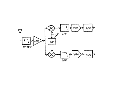
(0003] Fig. 1 shows one wireless application in the form of a cellular
communications receiver, which includes variable-gain amplifiers along its
signal
path. The receiver includes an antenna 1, an RF bandpass filter 2, and a low-
noise
amplifier 3. The signal output from the low-noise amplifier is combined, in
mixers
4 and 5, with phase-shifted versions of an oscillator signal. In this
receiver, the
oscillator signal is set to the carrier frequency and thus baseband-signal
recovery is
performed using one conversion. (A receiver of this type is often referred to
as a
direct-conversion receiver.) The output of each mixer is passed through a low-
pass filter LPF, amplified by a variable-gain amplifier VGA, and converted
into a
digital signal by an ADC converter. Subsequent signal processing steps are
then
p erformed.
1
CA 02559169 2006-09-11
WO 2005/086957 PCT/US2005/008197
(0044] In dixect-conversion and other types of receivers, variable-gain
amplifiers are used to suppress noise introduced into the baseband signal
along
the receiver signal path. The amount of noise suppression that takes place is
typically proportional to the gain of the amplifier. ~Xlhen the received
signal level is
smaller than desired, the gain of the amplifier is increased. Conversely, when
the
received signal level is higher than desired, the gain of the amplifier is
decreased.
By adjusting the gain of the amplifier and accordingly the level of the
baseband
signal, excessive constraints on the dynamic range of subsequent stages of the
receiver (including the analog-to-digital converter) can be avoided.
(0005] In wireless applications implemented using variable-gain amplifiers,
increasing amplifier linearity is considered important for obtaining an
acceptable
signal-to-noise ratio. Unfortunately, when these amplifiers lack sufficient
linearity,
the desired signal is corrupted by inter-modulation caused by strong
interfering
signals.
(0006] Fig. 2 has two signal diagrams which show, by comparison, one way
in which interference can affect the signals in a wireless application. The
first
signal diagram shows the state of a signal in a communications receiver such
as
shown in Fig. 1 prior to being input into one of the variable-gain amplifiers.
This
signal includes a desired signal and multiple interfering signals which have
substantially the same amplitudes propagating along the signal path. When the
desired and interfering signals have small magnitudes, the desired signal can
be
amplified to a desired level in spite of any linearities that may exist in the
VGA.
This is shown in the second signal diagram, where the amplitude of the desired
signal is greater than the amplitudes of interfering terms generated by inter-
modulation with the interfering signals. (In Fig. 2, Ps;g represents baseband
signal
power, which is shown to be triangular in shape and where the height of the
triangle is directly proportional to the power).
(0007] Fig. 3lhas two signal diagrams which show, by comparison, another.
way in which interference can affect the signals in a wireless application.
The first
signal diagram shows the state of a signal in a communications receiver such
as
2
CA 02559169 2006-09-11
WO 2005/086957 PCT/US2005/008197
shown in Fig. 1 prior to being input into one of the variable-gain amplifiers.
However, unlike Fig. 2, the interfering signals have significantly larger
amplitudes
than the desired signal. Consequently, when amplified by a variable-gain
amplifier
having non-linear characteristics, the desired signal is seriously corrupted
by noise
terms generated from inter-modulation with the interfering signals. This is
shown
in the second diagram, where the amplitudes of the noise terms are much
greater
than the desired signal amplitude. If left uncompensated, this noise will
propagate
throughout the receiver to degrade the quality of the received signal.
[0008 Fig. 4 shows a variable-gain amplifier which has been proposed for
use in a receiver. The amplifier is formed from a single differential
amplifier 50
which includes two feedback paths 51 and 52, four resistors, and a virtual
ground
provided at the amplifier inputs. Resistors R1 axe placed at the inverting and
non-
invexting terminals and resistors R2 are located along the feedback paths. The
values of resistors R1 and R2 control the gain of the amplifier, i.e., changW
g the
values of variable resistors R1 and R2 will result in setting the amplifier to
a
desired gain as indicated by the following equation:
VouT ' , VOUTB- R (ViN - V~Ne) ( 1 )
[0009 where Vout and Vo"rs axe the differential output voltages of the
amplifier, V;n and V;ns are the differential input voltages, and the ratio of
Ra and
R1 defines the gain.
[0010) Equation (1) defines the gain of the amplifier under ideal
operational characteristics. In practice, however, the gain is not infinite
and the
amplifier suffers from secondary effects. For example, because the amplifier
gain
is not infinite, the input nodes of the amplifier will slightly track the
input signal.
The amount of fluctuation that occurs at the inputs depends on the gain and
frequency characteristics of the amplifier.
[0011] Fig. 5 shows a block diagram of the operational trans-conductance
amplif er of Fig. 4. As shown, this amplifier may be modeled using five
transistors,
where the gates of transistors M1 and M2 receive respective differential
inputs IN and
3
CA 02559169 2006-09-11
WO 2005/086957 PCT/US2005/008197
INB, the gates of transistors M3 and M4 receive a control signal from common
mode
feedback circuitry (CMFB), and transistor MS is provided to set the bias
current of the
operational amplifier from the external bias circuitry not shown in Fig. 5.
The
common mode feedback circuit is used to stabilize the common mode output
voltage
of the two output signals, OUT and OUTB. Nodes N1 and N2 respectively disposed
between transistor pair Ml and M3 and transistor pair M2 and M4 provide the
differential output voltages OUT and OUTB of the amplifier. These voltages are
fed
back to the CMFB, where they are used to set the common mode output voltage of
the
two output signals. Ml, M2, and MS are NMOS transistors, M3 and M4 are PMOS
transistors, and VDD is a supply voltage connected to the sources of
transistors M3 and
M4.
[0012] The non-linear properties of the amplifier are mostly attributable to
the
common source node (A) of the input transistors. More specifically, since the
amplifier is usually designed to have very high gain at its input stage, small
distortion
at the input stage generates large distortion at the output stage. This large
distortion
results from the transient behavior node A experiences as a result of the two
current
signals flowing in the opposite directions (this opposing flow is explained in
greater
detail below). As a result, harmonics are generated at node A which alter the
linear
characteristics of the amplifier and thus generate the large distortion that
occurs at the
amplified output. The currents signals may be explained in greater detail as
follows. '
[0013] Since the two input signals, IN and INB, operate as a differential
signal
from the centered common mode signal, the two inputs signals can be expressed
as
follows:
~IN - ~CM ~
v
Y~Na - ~cM - 2
[0014] where VIM is defined by the common mode feedback circuit. Thus,
when the input voltage increases, the voltage of INB decreases. With this
condition,
the relative change of the current flowing into Ml and M2 transistors will
have
4
CA 02559169 2006-09-11
WO 2005/086957 PCT/US2005/008197
different polarity; that is, when the current in M1 increases the current in
M2
decrease, and when the current in M1 decreases the current in M2 increases.
The two
current signals into the M1 and M2 transistors may therefore be said to
flowing in
opposite directions.
(0015) Another source of non-linearity in the amplifier of Fig. 5 is the
common mode feedback circuitry While this circuitry is beneficial for purposes
of stabilizing the output levels of the amplifier, it produces mixed harmonics
which cause distortions in the output signal.
SUMMARY OF THE INVENTION
(0016] An object of the present invention is to provide a variable-gain
amplifier which has improved linearity characteristics compared with other
types
of amplifiers which have been proposed.
(0017) Another object of the present invention is to achieve the
aforementioned object by reducing the generation of harmonics and other forms
of noise that cause distortion in the amplifier output.
(001~J Another object of the present invention is to achieve one or more
of the aforementioned objects by eliminating common source node connections
that serve as a principal source of nonlinear distortion in other variable-
gain
amplifiers which have been proposed.
(0019] Another object of the present invention is to achieve one or more
of the aforementioned objects by eliminating common mode feedback circuitry
which also serves as a principal source of nonlinear distortion in other
variable-
gain amplifiers which have been proposed.
(0020) Another object of the present invention is to provide a
communications receiver which uses the aforementioned variable-gain amplifier
for baseband signal recovery, and/or to perform one or more other signal
processing functions.
CA 02559169 2006-09-11
WO 2005/086957 PCT/US2005/008197
[0021) Anothex object of the present invention is to provide a
communications receivex which includes a variable-gain amplifier as previously
described.
[0022) Another object of the present invention is to provide a method for
amplifying signals using a cixcuit which achieves one or more of the
aforementioned objects.
[0023) These and other objects and advantages are achieved by providing a
variable-gain amplifier circuit which according to one embodiment includes a
first
amplifier for amplifying a frst input signal and a second amplifier for
amplifying a
second input signal. The first and second input signals are preferably
different
portions of a single differential input signal, and the first and second
amplifiers output
different portions of a same differential output signal.
[0024) The amplifier circuit may also include a first node for inputting the
first input signal into the first amplifier and a second node for inputting
the second
input signal into the second amplifier, wherein current flow into the first
and second
nodes tracks each other to thereby reduce generation of harmonic components in
the
first and second input signals. Preferably, the direction of current flow into
the first
and second nodes is the same direction. Also, the first and second amplifiers
are
preferably single-output operational amplifiers.
[0025) The first amplifier may also include a non-inverting terminal which
receives the first input signal and the second amplifier includes an inverting
terminal
which receives the second input signal. A first node connected to the
inverting
terminal of the first amplifier is also connected to an output of the first
amplifier and
the non-inverting terminal of the second amplifier. Resistive elements are
preferably
disposed along signal paths between the first node and the non-inverting
terminal of
the second amplifier and along a feedback signal path between the first node
and the
output of the first amplifier.
[0026) The amplifier circuit may also include a second node connected to the
non-inverting terminal of the second amplifier, which is also connected to an
output
of the second amplifer and to the inverting terminal of the first amplifier.
Resistive
elements are preferably disposed along signal paths between the first and
second
6
CA 02559169 2006-09-11
WO 2005/086957 PCT/US2005/008197
nodes and along a feedback signal path between the second node and the output
of the
second amplifier.
[0027] Preferably, the first and second amplifiers are integrated to include a
current mirror, a first transistor having a gate for receiving the first input
signal, and a
second transistor having a gate for receiving the second input signal. Sources
of the
first and second transistors are connected to form a common node and drains of
the
first and second transistors are connected to the current mirror.
Complementary output
nodes are respectively disposed between the current mirror and the first and
second
transistors.
[0028] The variable-gain amplifier of the present invention achieves
improved linearity compared with other VGAs which have been proposed. These
VGAs use a single differential operational amplifier which is non-ideal in
terms of
producing a linear characteristic and which also uses convnon mode feedback
circuiriy which has been shown to introduce noise into the amplifier output.
The
present invention overcomes these drawbacks by replacing the differential
operational amplifier with two single-ended operational amplifiers, each of
which
is connected to receive a respective one of two differential input signals.
Through
this design, linearity is greatly improved and the use of common mode feedback
circuitry can be avoided, both of which translate into improved signal quality
in
the amplifier output.
BRIEF DESCRIPTION OF THE DRAWINGS
[0029] Fig. 1 shows a dixect-conversion receiver.
[0030] Fig. 2 shows input and output signal waveforms for a variable-gain
amplifier under a ftxst set of conditions.
[0031] Fig. 3 shows input and output signal waveforms for a variable-gain
amplifier under a second set of conditions.
[0032] Fig. 4 shows one type of vaxiable-gain amplifier which has been
proposed.
[0033] Fig. 5 shows a circuit diagram for the amplifier shown in Fig. 4.
7
CA 02559169 2006-09-11
WO 2005/086957 PCT/US2005/008197
(0034j Fig. 6 shows a variable-gain amplifier in accordance with a preferred
embodiment of the present invention.
(0035] Fig. 7 shows a preferred circuit diagram of single-ended operational
amplifiers included in the variable-gain amplifier of Fig. 6.
DETAILED DESCRIPTION OF PREFERRED EMBODIMENTS
(0036] Fig. 6 shows a variable-gain amplifier in. accordance with a preferred
embodiment of the present invention. This amplifier includes first and second
single-ended operational amplifiers 100 and 110 and three variable resistors
120,
130, and 140. The non-inverting terminals of the first amplifier and second
amplifiers axe connected to receive differential input signals IN and INB
respectively. The inverting terminal of the first amplifier is connected to
the
output OUT of amplifier 100 through a feedback path which includes resistor
120, and the inverting terminal of the second amplifier is connected to the
output
OUTB of amplifier 110 through a feedback path which includes resistor 130.
Resistors 120 and 130 preferably have the same resistance values.
(0037] The non-inverting of the first amplifier and the non-invertijig
terminal of the second amplifier are coupled to one another through resistor
140,
which is preferably different in value from the other two resistors. More
specifically, as shown in Fig. 6, node A connects the non-inverting terminal
of
amplifier 100 to resistor 140 and the feedback signal output from resistor
120.
Node B connects the inverting terminal of amplifier 110 to resistor 140 and
the
feedback signal output from resistor 130. In this arrangement, resistor 140
along
with resistors 120 and 130 perform the gain function as indicated in Equation
(2)
discussed below.
(0038] The variable-gain amplifier of the present invention represents a
significant improvement in the art. By using two single-ended operational
amplifiers instead of one differential amplifier as shown in related-art Fig.
4, the
present invention is able to achieve substantially better linearity
characteristics.
Also, because the amplifier of the invention is implemented without common
8
CA 02559169 2006-09-11
WO 2005/086957 PCT/US2005/008197
mode feedback circuitry, the generation of harmonics and other forms of noise
which introduces distortion and overall tends to degrade signal quality is
significantly reduced. These benefits are explained iiz greater detail as
follows.
[0039] A main cause of the non-linearity in related-art variable-gain
amplifiers is that harmonic components introduced into the input signal are
translated
into large harmonic distortion in the output signal. The present invention
reduces or
altogether eliminates this problem by replacing the differential amplifier
with two
single-ended amplifiers. In this configuration, the direction of current flow
in the two
input nodes track each other and therefore a significant reduction in the
generation of
harmonic components at the amplifier input is realized. Arrows 125 and 135 are
provided to show the directions of flow of the current signals input into the
amplifier,
i.e., these arrows show the current flow directions when the voltage of the TN
signal
increases and the voltage of the INB signal decreases.
[0040] Fig. 7 shows a preferred circuit diagram of the single ended
amplifiers used in Fig. 6. This diagram includes five transistors, three of
which
M1, M2, and M5 axe preferably implemented in NMOS and the remaining two
'M3 and M4 in PMOS. The gates of transistors M1 and ~-M2 are connected to
receive differential input signals IN and INB. Assuming that the voltage of IN
signal is larger than that of the INB signal, the voltage of the OUT signal
will
increase and the voltage of the OUTB signal will decrease. This is evident
from
the operating principles of the operational amplifier.
[0041] When the voltage at the IN node increases, the current flowing in the
M1 transistor increases. Then, this current is sourced into the OUT node by
the
current mirror formed by coupled transistors M3 and M4. This operation is
applied to
the operation of the variable-gain amplifier of the present invention.
[0042] More specifically, referring to Fig. 6, as the positive voltage input
into
the IN node increases, the signal .from the OUT node increase. This increase
in
voltage from the OUT node, in turn, causes the voltage at node A (the
complementary
input node of amplifier 100) to increase by the feedback resistor 120. In
controlling
the voltage at node A and the voltage output from the OUT node, the ratio
between
9
CA 02559169 2006-09-11
WO 2005/086957 PCT/US2005/008197
resistors R1 and R2 sets the gain, for example, in the manner indicated in
Equation
(2).
[0043] The large gain of the operational amplifier enables the voltages at
node
A and the input node IN to become the same. Similarly, the voltages at node B
and
input node INB become the same. A steady-state condition is therefore reached
in
which the output voltage of the variable-gain amplifier may be expressed by
the
following equation:
Vour - Voura= R (Vw - Vwe) (2)
[0044] A comparison of Equations (1) and (2) reveals that the gain of the
variable-gain amplifier of the related are and the present invention may be
the same.
However, unlike the related-art amplifier, the two input nodes IN and TNB of
the
amplifier of the present invention track one other and thus harmonic
components
generated at common source node C in Fig. 7 is minimized or altogether
eliminated.
As a result, harmonic distortion at the output nodes OUT and OUTB of the
variable-
gain amplifier of the present invention is greatly reduced.
[0045] Another advantage of the variable-gain amplifier of the present
invention is that it does not require common mode feedback circuitry. By
comparison,
in the amplifier of Fig. 4, the input common mode gain is very small, which
means
that any offset in the operational amplifier can cause large offset to occur
at the output
nodes of the VGA. This common gain is inversely proportional to the drain-
source
resistance of transistor MS in Fig. 4, which is usually very large.
Consequently,
common gain is quite small. '
[004G] In contrast, in the variable-gain amplifier of Fig. 6, the OUT signal
has
the same common mode voltage as the IN signal, and the OUTB signal has the
same
common mode voltage as the INB signal. This feature eliminates the necessity
of
using common mode feedback circuitry, which, in turn, translates into improved
linearity characteristics of the variable-gain amplifier by removing the
harmonic
distortion that otherwise would have been generated by the common mode
feedback
circuitry.
CA 02559169 2006-09-11
WO 2005/086957 PCT/US2005/008197
[0047] The present invention is also a communications receiver which
includes a variable-gain amplifier according to any of the embodiments
described
herein. Preferably, the receiver includes the variable-gain amplifier along a
signal
path of the front end of the receiver where baseband signal recovery takes
place. In
this configuration, the amplifier of the present invention may be connected to
the
output of one or more mixers used to recover the baseband signal from a
received
signal. The receiver may be a direct-conversion receiver having the same
general
architecture shown in Fig. 1, a superheterodyne receiver, or any other
receiver
conftguration.
[004] The foregoing embodiments and advantages are merely exemplary
in nature and are not to be construed as limituig the present invention. The
present teachings can be readily applied to other types of apparatuses.
Moreover,
the description of the present invention provided herein is intended to be
illustrative and not to be limiting of the scope o~ the claims. Many
alternatives,
modifications, and variations will be apparent to those skilled in the art.
11