Note: Descriptions are shown in the official language in which they were submitted.
CA 02559171 2006-09-08
WO 2005/089945 PCT/US2005/008248
Nanoliter Array Loading
[0001] Field of the Invention
[0002] The invention generally relates to techniques for assaying sample
liquids, and more
specifically to techniques for utilizing a sub-set of nanoliter sample volumes
in an array.
Background Art
[0003] Various systems are known for performing a large number of chemical and
biological storage assays and synthesis operations. One approach uses an assay
chip
having an array of nanoliter volume through-hole sample wells with hydrophilic
interiors
io and openings surrounded by hydrophobic material. One specific commercial
example of a
nanoliter chip system is the Living ChipTM made by BioTrove, Inc. of Woburn,
MA.
Nanoliter chip technology relies on the ability to handle very small volumes
of fluid
samples, typically, 100 nanoliters or less. The various considerations taken
into account in
handling such small liquid samples are known as microfluidics.
[0004] Figure 1 shows a cut away view of a typical nanoliter sample chip. This
is
described, for example, in U.S. Patent 6,387,331 and U.S. Patent Application
20020094533, the contents of which are incorporated herein by reference. Array
chip 10
contains an array of through-hole sample wells 12 that traverse the chip 10
from one
2o planar surface 14 to the other opposing planar surface (not shown).
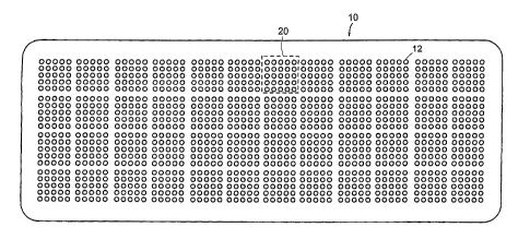
[0005] The sample wells 12 may be grouped into sub-arrays such as by
controlling the
spacing between the wells. For example, Figure 2 shows a chip 10 in which the
sample
wells 12 are grouped into a 4 by 12 array of 5-well by 5-well sub-arrays 20.
In another
embodiment, the sub-arrays 20 may be 8-wells by 8-wells or any other
convenient
number. The chip 10 in Fig. 2 is 1" x 3" to correspond to a standard
microscope slide. The
sample wells 12 in a sub-array 20 may be laid out in a square or rectangular
grid
arrangement as shown in Fig. 2, or the rows and/or columns of sample wells may
be offset
as shown in Fig. 1.
-1-
CA 02559171 2006-09-08
WO 2005/089945 PCT/US2005/008248
[0006] The sample chip 10 typically may be from 0.1 mm to more than 10 mm
thick; for
example, around 0.3 to 1.52 mm thick, and commonly 0.5 mm. Typical volumes of
the
through-hole sample wells 12 could be from 0.1 picoliter to 1 microliter, with
common
volumes in the range of 0.2-100 nanoliters, for example, about 35 nanoliters.
Capillary
action or surface tension of the liquid samples may be used to load the sample
wells 12.
For typical chip dimensions, capillary forces are strong enough to hold
liquids in place.
Chips loaded with sample solutions can be waved around in the air, and even
centrifuged
at moderate speeds without displacing samples.
[0007] To enhance the drawing power of the sample wells 12, the target area of
the
receptacle, interior walls 42, may have a hydrophilic surface that attracts a
sample fluid. Tt
is often desirable that the surfaces be bio-compatible and not irreversibly
bind
biomolecules such as proteins and nucleic acids, although binding may be
useful for some
processes such as purification and/or archiving of samples. Alternatively, the
sample wells
12 may contain a porous hydrophilic material that attracts a sample fluid. To
prevent
cross-contamination (crosstalk), the exterior planar surfaces 14 of chip 10
and a layer of
material 40 around the openings of sample wells 12 may be of a hydrophobic
material
such as a monolayer of octadecyltrichlorosilane (OTS). Thus, each sample well
12 has an
interior hydrophilic region bounded at either end by a hydrophobic region.
[0008] The through-hole design of the sample wells 12 avoids problems of
trapped air
inherent in other microplate structures. This approach together with
hydrophobic and
hydrophilic patterning enable self-metered loading of the sample wells 12. The
self-
loading functionality helps in the manufacture of arrays with pre-loaded
reagents, and also
in that the arrays will fill themselves when contacted with an aqueous sample
material.
[0009] It has been suggested that such nanoliter chips can be utilized for
massively
parallel assays such as Polymerase Chain Reaction (PCR) and Enzyme-Linked
Immunosorbent Assay (ELISA) analysis. However, one problem with such
applications of
so nanoliter chips is the complex time-consuming preparation and processing of
the chip that
is required. Before the samples are introduced, each sample well must be pre-
formatted
with the necessary probes, reagents, etc., which will be referred to generally
as reagents.
-2-
CA 02559171 2006-09-08
WO 2005/089945 PCT/US2005/008248
Such chip preparation will be referred to as formatting. Once the chip is
formatted, the
analyte or specimen must be introduced into each well, which will be referred
to as sample
loading. The term sample will be used to refer generically to both specimens
and reagents.
Transferring of large collections of fluid samples such as libraries of small
molecule drug
candidates, cells, probe molecules (e.g., oligomers), and/or tissue samples
stored in older
style 96- or 384-well plates into more efficient high density arrays of
nanoliter receptacles
can be difficult. As a practical matter, there tend to be two approaches to
formatting and
loading of nanoliter sample chips - bulk transfer and discrete transfer.
io [0010] An example of bulk transfer is dipping a sample chip into a
reservoir of sample
liquid. The sample liquid wicks into the sample wells by capillary action and
all of the
wells fill uniformly with the sample.
[0011] One established method for discrete transfer uses a transfer pin loaded
with the
15 transfer liquid. For example, pins or arrays of pins are typically used to
spot DNA samples
onto glass slides for hybridization analysis. Pins have also been used to
transfer liquids
such as drug candidates between microplates or onto gels (one such gel system
is being
developed by Discovery Partners, San Diego, CA). Many pin types are
commercially
available, of various geometries and delivery volumes. V&P Scientific of San
Diego, CA
2o makes slotted, grooved, cross-hatched, and other novel-geometry pins. The
Stealth Pin by
ArrayIt is capable of delivering hundreds of spots in succession from one
sample uptake,
with delivery volumes of 0.5nL to 2.5nL. Majer Precision Engineering sells
pins having
tapered tips and slots such as the MicroQuil 2000. Techniques for using a one
or more pins
to transfer sample liquid are described in U.S. Patent Application 101227,179,
filed August
25 23, 2002, and incorporated herein by reference.
Summary of the Invention
[0012] Representative embodiments of the present invention include methods and
systems
for providing an interface for storing microfluidic samples in a nanoliter
sample chip. A
so fluid access structure provides a fluid access region to a selected subset
of sample wells
from an array of sample wells. A fluid introduction mechanism introduces a
sample fluid
to the fluid access region so that the sample wells in the selected subset are
populated with
-3-
CA 02559171 2006-09-08
WO 2005/089945 PCT/US2005/008248
the sample fluid without the unselected sample wells being populated with the
sample
fluid.
[0013] In further embodiments, the fluid access structure may be adapted for
positioning
next to a planar surface of the array to provide the fluid access region. The
fluid access
structure may include at least one nnicrofluidic circuit for distributing the
sample fluid to
the fluid access region, which may be fixed to the array or detachable from
the array.
(0014] In another embodiment, the fluid access structure may be adapted to
fold a portion
to of the array to provide the fluid access region. For example, the fluid
access structure may
be adapted to fit into a microplate sample well so as to enable introducing a
sample fluid
within the microplate sample well into the fluid access region.
[0015] In other embodiments, the fluid access structure may include a mask to
create a
15 barrier between the fluid access region and the rest of the array. Or a
printing plate may be
used as the fluid access structure and the fluid introduction mechanism. The
fluid
introduction mechanism may be based on dragging a drop of the sample fluid
over the
fluid access region. Or the fluid introduction mechanism may be adapted for
dispensing a
focused drop of the sample fluid into the fluid access region, such as by
spraying. In
2o various embodiments, a sponge or a pipette may be used for the fluid
introduction
mechanism.
[0016] In another embodiment, a membrane is used as the fluid access structure
and fluid
introduction mechanism. The membrane may include an outer surface having
patterned
25 hydrophobic and hydrophilic regions
[0017] Embodiments also include a leit for storing microfluidic samples. The
lit contains
any of the interfaces described above as well as a chip containing the array
of sample
wells. In such a kit, the interface may further contains a reagent for the
wells in the
so selected subset of sample wells. For example, the reagent may be a dye for
staining the
sample fluid populated into the subset of wells.
-4-
CA 02559171 2006-09-08
WO 2005/089945 PCT/US2005/008248
Brief Description of the Drawings
[0018] Figure 1 shows a detailed cut away view of a typical nanoliter sample
chip
according to the prior art.
[0019] Figuxe 2 shows a top plan view of a chip according to Figure 1 in which
the array
of sample wells is grouped into sub-arrays.
[0020] Figure 3 shows various details of channel geometry for use in a fluid
access
structure.
[0021] Figure 4 shows a cross section of a PDMS loader interface according to
one
embodiment of the present invention.
[0022] Figure 5 shows a PDMS loader interface having a hard plastic over-layer
according
to one embodiment.
[0023] Figure 6 shows an alternative embodiment of a PDMS loader interface
with a hard
plastic over-layer.
[0024] Figure 7 shows an embodiment in which a portion of the sample chip is
folded to
enable a sub-array to fit into a sample well of a microplate array.
[0025] Figure 8 shows a mask-based embodiment of an interface loader.
[0026] Figure 9 shows use of contact printing as an interface loader
mechanism.
[0027] Figure 10 shows an embodiment in which a porous membrane serves as an
interface loader mechanism.
Detailed Description of Specific Embodiments
[0028] Various embodiments of the present invention are directed to providing
an
-5-
CA 02559171 2006-09-08
WO 2005/089945 PCT/US2005/008248
interface for storing microfluidic samples in an array of through-hole sample
wells. A
fluid access structure provides a fluid access region to a selected subset of
sample wells. A
fluid introduction mechanism introduces a sample fluid to the fluid access
region so that
the sample wells in the selected subset are populated with the sample fluid
without the
unselected sample wells being populated with the sample fluid.
[0029] A variety of factors affect how specific embodiments are realized.
Among these is
the need for uniformity - the specific process should approach the uniformity
of batch
loading techniques, with minimal fluidics errors (e.g., less than 1% of the
selected sample
io wells fail to properly load the sample fluid). Also, dead volume (unused
sample fluid left
in the loading interface) should be minimized to the extent possible; in
efficient
embodiments, dead volume may be less than 10/0 of the total sample fluid
volume. In
addition, cross-contamination (cross-talk) needs to be avoided between the
selected
sample wells and the unselected sample wells.
[0030] Other factors that influence specific embodiments include specific
details of the
intended application. For example, whether manual loading or robotic loading
will be used
to provide sample fluid to the fluid introduction mechanism, the sample source
structure
(e.g., 384-well microplate), and compatibility with other handling procedures
such as use
of perfluorinated liquids. Also, the amount of space between adjacent sub-
arrays affects
susceptibility to cross-talk.
[0031] After the sample fluid has been loaded into the wells in the subset
(sub-array), the
loader interface containing the fluid access structure and the fluid
introduction mechanism
may be removed, for example by peeling or prying it off the surface of the
sample chip. In
one embodiment, the sample chip and loader interface come packaged together as
a kit in
which the loader interface is pre-affixed to the sample chip ensuring proper
alignment
between the two. In some specific embodiments, it may be useful to provide
reagents in a
dry form on the walls of the interface loader structures. Structures
associated with a given
so sub-array may have the same reagent or different reagents. The reagents may
be
encapsulated in a gel or wax such as polyethylene glycol (PEG). For example, a
fluorescent dye may be coated on the interior walls of a loader interface so
that when a
-6-
CA 02559171 2006-09-08
WO 2005/089945 PCT/US2005/008248
biochemical sample such as nucleic acids, cells, or proteins are added to a
given sub-array,
they are stained with the dye.
[0032] In one specific embodiment, the fluid access structure is adapted for
positioning
next to a planar surface of the sample chip to provide the fluid access
region, for example,
by providing at least one microfluidic circuit for distributing the sample
fluid to the fluid
access region. Such a microfluidic circuit may be based on microfluidic
channels in the
fluid access structure such that the channels overlay and connect the openings
of the
subset of sample wells in the fluid access region. The fluid introduction
mechanism may
to be a port or reservoir that supplies sample fluid to the channels. For
example, a pipette or
micro-syringe may provide sample fluid to a fluid introduction mechanism such
as a
docking port that receives the sample fluid. The docking port connects with
the access
structure channels that form the fluid access region. The sample fluid in the
channels then
is populated into the selected subset of sample wells in the sample chip. In
various
15 embodiments, there may be one docking port per channel, or a plurality of
docking ports
per channel.
[0033] The microfluidic channels, while open on the bottom side that faces the
sample
chip, may be either closed or open on top. Channels that are open on the top
have the
2o advantage of being easier to load by hand or with a robotic dispensing
station having
ordinary precision, since a droplet need only contact the microfluidic circuit
fluid access
structure at any position on the structure. Open-top structures are typically
easily produced
from rigid materials such as steel, titanium, glass or silicon but these rigid
structures may
be expensive as in the case of silicon, or of insufficient flatness and
flexibility to provide
25 intimate contact with the underlying array as in the case of steel. A
closed-top structure
may be easier to manufacture from elastomeric materials, but may require the
use of ports
and docleing of dispensers to those ports as well as regulation of the
pressure applied by
the dispensers. The fluid access structure may be produced from various
materials,
including without limitation metal, plastic, and glass. In one specific
embodiment, silicon
so was used to fabricate the fluid access structure and was found to be easy
to handle, with
good rigidity, but also relatively fragile, easily breakable, and expensive to
produce. One
way to benefit from the rigidity and open top design of hard materials with
the intimate
CA 02559171 2006-09-08
WO 2005/089945 PCT/US2005/008248
fluidic contact of soft or elastomeric materials is to coat a structure
produced with a hard
material such as steel with a soft material such as PDMS.
[0034] Another embodiment may be based on metal such as stainless steel. Steel
is easy to
handle, inexpensive, and possesses excellent rigidity and strength. Steel also
is
hydrophilic, which helps hold the sample fluid in the channels. To avoid cross-
talk, a steel
fluid access structure may include a hydrophobic monolayer surface coating,
such as of
octadecyItrichlorosilane (OTS). To promote good wetting properties and
biocompatibility
of the inside walls of a microfluidic circuit, these may be selectively coated
with a
io hydrophilic material. The hydrophilic material may, without limitation, be
a deposition of
hydrophilic and preferably biocompatible wax such as polyethylene glycol
(PEG), or a
covalently linked coating such as a silane bearing PEG moieties.
[0035] The channels in a steel fluid access structure can be produced by
various different
15 methods such as etching or Electrical Discharge Machining (EDM). EDM uses
high-
energy electric current to melt the base metal for burr-free machining. Wire
EDM can
produce intricate patterns and complex shapes with great precision and minimal
variation.
[0036] Figure 3A shows some examples of various channel shapes for use in a
fluid access
zo structure. The chip sample wells 12 are the small holes seen in Figure 3A.
Among the
channel shapes are a serpentine geometry 31, an irrigation row geometry 32,
and a spiral
geometry 33. There may be a fluid introduction mechanism such as a docking
port and
sample reservoir connected to a point in a given geometry. Then, the sample
fluid is
delivered from the fluid introduction mechanism to the microfluidic channels)
of the fluid
z5 access structure. As the sample fluid travels down the channel over the
opening of a
sample well, it is wicked into the well by capillary action to fill a volume
of the sample
well with the sample fluid.
[0037] Depending on the specific channel shape, and other factors such as the
geometry of
so the sample chip, the width of the fluid access structure channels needs to
be properly
dimensioned to be neither too narrow nor too wide. Fig. 3B and 3C show cross-
sectional
views of two different channels. Figure 3B shows a sample loader interface
that is 500 ~.m
_g_
CA 02559171 2006-09-08
WO 2005/089945 PCT/US2005/008248
thick having a 140 pm wide channel with perpendicular walls. Figure 3C shows a
sample
loader interface that is 300 ~,m thick having hourglass-shaped channel walls
that are 320
p.m thick at the center and 450 ~.m thick at the surface. In one specific
embodiment, the
width of the channels may be the same as the diameter of the sample well
openings. In
another embodiment, the channels are narrower than the diameter of the sample
well
openings. In some geometries, thinner channels may be preferred as providing
better
sample transfer characteristics, and channels that are too wide may have
problems filling
spontaneously with sample fluid from a pipette, or may not transfer sample
fluid
efficiently to an adjacent sample chip. In some embodiments, the fluid access
structure is
io the same thickness as the sample chip, so that there is a 1:1 aspect ratio
between the
sample wells and the microcircuit channels, e.g., both the fluid access
structure and the
sample chip rnay be 300 ~.rn thick. Also the thicker the fluid access
structure is, the greater
the undesirable dead volume of untransferred sample f1W d may be. Thicker
fluid access
structures may also be harder to load with sample fluid.
[0038] It is important to obtain good planar surface contact between the
sample chip and
the fluid access structure. Poor contact may result in inconsistent loading
and other
problems. It rnay be more or less difficult to fabricate some materials in the
desired
geometries and dimensions with the necessary flatness and rigidity. Moreover,
some
2o materials may be more prone to being deformed when handled. Some materials
may have
issues with burrs and other fabrication irregularities that may interfere with
proper
operation.
[0039] One means to enhance contact is to apply pressure to press the sample
chip and the
fluid access structure together, for example by clamping_ In some embodiments,
magnetic
materials may assist in forming proper surface contact between the sample chip
and the
fluid access structure. Gaskets may also be useful for connecting the chip and
the fluid
access structure. For example, an elastomeric polymer such as
Polydimethylsiloxane
(PDMS) may be used as a gasket in some embodiments. In other embodiments, a
so sandwiched layer of PDMS usefully connects the planar surface of the sample
chip and the
fluid access structure.
-9-
CA 02559171 2006-09-08
WO 2005/089945 PCT/US2005/008248
[0040] In another embodiment, the sample loader interface itself may be based
on a
elastomeric material such as PDMS. That is, the channels of the fluid access
structure and
the sample receiving port of the fluid introduction mechanism may be cast in
PDMS.
PDMS is naturally soft and tacky, and it can cast fine features in the range
of 10-50 ~,m.
[0041] Figure 4 shows a cross section of a PDMS loader interface 40 having a
serpentine
geometry 31 as seen in Fig. 3A. Fig. 4A shows a cross-section of the fluid
introduction
interface which includes a docking port 41 into which a pipette or
microsyringe containing
the sample fluid may be inserted. At the bottom of the docking port 41 is a
sample
1o reservoir 42 which holds a volume of sample fluid for delivery into the
microfluidic
channels of the fluid access structure. Figure 4B shows a cross-section
through a
microfluidic channel 43 which overlays the openings of the sample wells in the
serpentine
geometry 31 shown in Fig. 3A. Thus, sample fluid from a pipette or
microsyringe in the
docking port 41 is delivered via the sample reservoir 42 to the microfluidic
channel 43. As
~5 the sample fluid travels down the channel 43 and passes over the opening of
a sample
well, it is wicked into the sample well by capillary action and the sample
well is populated
with a volume of the sample fluid. If the sample fluid is provided with too
much pressure,
some fluid may escape the reservoir 42 or channel 43 and cause cross-
contamination
(cross-talk).
[0042] A PDMS loader interface can conveniently be produced by casting polymer
resin
on a mold mask having the desired features and geometry. For example, a
prototype
interface can be produced in PDMS resin by using stereolithography to convert
three-
dirnensional CAD data into a series of very thin slices. A laser-generated
ultraviolet light
beam traces each layer onto the surface of the liquid polymer, forming and
hardening each
layer until the complete, full-size prototype is formed. Another technique for
forming a
polymer-based loader interface may use ultraviolet lithography to develop an
SU-8 photo
resist structure. It may be useful to experimentally vary the ratio of resin
base to
developer, as well as the settling and curing times and temperatures in order
to remove a
so cast interface from its mold without damage. In general, slower curing at
lower
temperature may work better, as higher temperature curing may cause the molded
interface to be too brittle. Access ports for the fluid introduction mechanism
can be
-10-
CA 02559171 2006-09-08
WO 2005/089945 PCT/US2005/008248
molded in, or added after molding by boring, laser machining, punching, or
drilling a hot
needle.
[0043] Although the channels of the loader interface need to be hydrophilic in
order to
properly transport and deliver the sample fluid, PDMS is naturally hydrophobic
and it
needs special treatment to become hydrophilic. It is known in the art to treat
PDMS with
plasma gas to change it from hydrophobic to hydrophilic. One drawback of
plasma
treatment is that it has been known to degrade over time to return back to its
natural state.
Another treatment approach is to deposit a hydrophilic coating on the channel
surfaces,
1o such as from a solution of polyethylene glycol (PEG). Another possibility
is a combined
treatment with plasma and PEG. By coating the interior surfaces as with PEG,
and then
allowing the other surfaces to revert to hydrophobicity or treating these
surfaces to render
them hydrophobic, a selectively coated elastomer structure results which may
be optimal
in both ease of loading and prevention of sample crosstalk.
[0044] In some applications, the soft resiliency of PDMS can cause problems
with the
fluid introduction mechanism, specifically, the docking ports may be difficult
to use. One
solution is to overlay the main PDMS structure with a layer of hard material
such as hard
plastic. Figure 5 shows such an embodiment in Which a hard plastic over-layer
50 lies on
2o top of a PDMS loader interface 40 and sample chip 10. The over-layer 50
includes an
oversize docking port 51 which by virtue of its larger size and harder plastic
material may
act more effectively to receive the end of a pipette or microsyringe
delivering the sample
fluid.
[0045] Figure 6 shows a further embodiment in which the hard plastic over-
layer 50 wraps
around the sides of the PDMS loader interface 40 and sample chip 10. This
configuration
can provide added stability and rigidity to the entire structure and help
maintain proper
registration (alignment) between the PDMS loader interface 40 and the sample
chip 10.
so [0046] Microfluidic circuits may also be used with other non-through-hole
rnicroarrays
including nucleic acid hybridization or protein arrays on glass slides.
Microfluidic circuit-
based fluid access structures may be very effective and may avoid many sample
transfer
-11-
CA 02559171 2006-09-08
WO 2005/089945 PCT/US2005/008248
problems such as smearing and blotching of sample fluid across the surface of
the sample
chip in and around the fluid access region. But microcircuits may wastefully
retain some
of the sample fluid in an unused dead volume.
s [0047] Another embodiment may be based on a three-dimensional structure
having sub-
arrays of sample wells to avoid such dead volume problems. A structure may be
adapted
to allow simultaneous access to the benefits of a high-density nanoliter array
format, and
the automated liquid-handling advantages of commercial microtiter plates.
Unlike the two-
dimensional planar nanoliter sample chip shown in Fig. 1, such embodiments are
three-
io dimensional with sub-arrays of sample wells connected to each other by a
structure that is
above the plane of the sample wells to facilitate mating with a microtiter
plate.
[0048] One difficulty in manufacturing such a microtiter-compatible loader
interface is
that techniques for producing the through-hole nanoliter sample wells require
the substrate
15 to be planar. One approach would be to micromold from a suitable polymer a
three-
dirnensionaI structure compatible with a standard size microtiter plate, the
micromolding
creating the desired through-hole nanoliter sample well geometry at the
correct locations
that will be mated with the microtiter plate. Alternatively, an embodiment
could be made
of multiple components that require assembly in order to generate the required
structure
2o for mating with a microtiter plate.
[0049] In another specific embodiment, a planar material such as a metal can
be etched
using conventional photochemical fabrication methods. Then two additional
folding steps
may be used to produce the required three-dimensional structure. With proper
design of
25 the initial planar part, the final fabricated structure can be made to
match with a microtiter
plate so that sub-arrays of sample wells fit inside the wells of the
microtiter plate. Such an
embodiment has the advantage of no assembly steps, together with the
reliability and
precision of photochemical etching, and the ease of forming thin sheet metal.
ao [0050) Figure 7A shows the initial etched planar piece of such a foldable
loader interface
70. The structure arms in Fig. 7A will ultimately become the fluid
introduction mechanism
71 for introducing the sample fluid in the microtiter plate wells to the fluid
access regions
-12-
CA 02559171 2006-09-08
WO 2005/089945 PCT/US2005/008248
72 that are the nodes in Fig. 7A. The fluid access regions 72 shown in Fig. 7A
each have a
5x5 sub-array of 25 through-hole nanoliter sample wells 12 for holding the
sample fluid
from the fluid access regions that are the microtiter plate wells. The number
of sample
wells in each sub-array can be easily changed changing the size of the node.
If the sample
wells are etched at a higher density, 1000 or more sample wells per node is
possible. In the
interface 70 shown in Fig. 7A, there are 96 nodes (though 384 would be equally
easy to
manufacture). The work piece shown in Fig. 7A is the interface 70 after
photochemical
etching, but before forming. The outside frame could be removed before the
forming
operations, or it could be left attached and used to handle the final part.
[0051] The interface 70 shown in Fig. 7A can be finished by using two forming
dies that
are designed so that they each act on only one direction of the woxk piece.
The first
forming operation would then bend the all of the material in one direction -
for example,
all rows - and leave the material connections on the columns undisturbed. An
example of
a portion of the resulting work piece is shown in close-up in Fig. 7B. The
final forming
operation would be orthogonal to the first to then shape all of the columns. A
portion of
the final formed interface 70 would be as shown in the close-up in Fig. 7C.
The final
formed interface 70 structure can then match the top of a standard 96-well
microtiter
sample plate. This allows the nanoliter-size sample wells in the sub-arrays of
each fluid
2o access region 72 to be inserted and withdrawn numerous times into the wells
of a
microtiter plate (as well as various other liquid receptacles) in order to
perform various
steps in one or more assay operations.
[0052] To use such a three-dimensional loader interface, reagents can be pre-
formatted
into the sample wells of the unformed planar work piece, for example, using
pin transfer
technology. Alternatively, the interface 70 may first be formed into its final
shape, and
then inverted to allow reagents to be transferred into the sample wells by pin
transfer. The
transferred reagents may be fixed onto the walls of the sample wells by
drying, and then
released upon dipping the interface 70 into a microplate with sample fluid in
its wells. In
so the specific case of PCR, thermal cycling would follow. Wash operations may
also be
performed by dipping the assembly into a trough or a microplate as for an
ELISA. After
performing analytical reactions, the plate may be imaged with a laser scanner
or high
-13-
CA 02559171 2006-09-08
WO 2005/089945 PCT/US2005/008248
resolution CCD-based system in any available readout mode.
[0053] There are also a variety of other approaches to provide a sample loader
interface to
a sample chip. Figure 8 shows an embodiment in which the fluid access
structure and fluid
introduction mechanism are integrated together into a mask overlay. A
resilient material
such as PDMS or silicone divides the surface of the sample chip by creating
fluid barriers
between sub-arrays. In a mask-type application, it may b a useful to place the
sample chip
onto a hydrophobic surface to prevent the sample fluid from spreading across
the bottom
of the chip. Alternatively or in addition, various embodiments may employ a
mask on the
1o top of the sample chip and a similar corresponding mask. on the bottom of
the sample chip
to avoid cross-talk. Chips intended for use with sub-array masks may also have
ridges and
other surface features such as spacing arrangements to aid with registration
of the mask
with the sample chip.
[0054] It may also be useful to blot the surface of the ch>Ep after adding
sample fluid to one
of the sub-arrays. For example, a serpentine loader circuit such as shown in
Fig. 3A may
be laid over the sub-array filled using the mask in order to blot up excess
sample fluid.
Mask-based embodiments may have difficulties with blotching of the sample
fluid leading
to cross-talk. The mask is typically removed from the array after blotting and
prior to use.
[0055] Masking performance may also be improved by using a centrifuge loading
technique. In addition or alternatively, sample fluid may be introduced into a
masked sub-
array by a variety of means including without limitation use of a swab, brush,
pad, or
sponge.
[0056] Figure 9 shows another embodiment in which the sample fluid is
transferred to a
selected sub-array of sample wells by printing. As shown in Fig. 9A, a
hydrophilic island
91 in a background of hydrophobic areas on a printing plate 90 is loaded with
sample fluid
92, for example by use of a pipette. The printing plate 90 is then pressed
down into contact
so with the openings of a selected set of sample wells 12 in a sub-array on
sample chip 10.
Sample liquid is then wicked by capillary action into the= selected sample
wells 12 and the
printing plate 90 is lifted off of the sample chip 10. As pith mask-based
embodiments, it
-14-
CA 02559171 2006-09-08
WO 2005/089945 PCT/US2005/008248
may then be useful to blot the surface of the sub-array, for example with a
serpentine
circuit interface, to remove any excess sample liquid from the surface of the
sub-array. In
some printing-based embodiments, it may be difficult to prevent spreading of
the printed
sample fluid which could lead to cross-talk. Other potential problems include
difficulties
aligning the printing plate 90 with the sample chip 10, the mufti-step nature
of the printing
process, and general messiness in the process.
[0057] Transferring sample fluid by dragging a hanging drop across the surface
openings
of selected sample wells may be useful either in combination with various of
the above
yo embodiments, or on its own. A pipetter, capillary tube, microsyringe,
cannula, pin, or the
like may be used to dispense and drag droplets across selected sub-arrays.
This may be
aided by use of a liquid handling station such as a reformatter,
BioMekTM(marketed by
Beckman Coulter of Fullerton, CA), or other commercial system. For example, a
sample
chip may be positioned beneath an array of hanging drops in a jig that
confines the
is movement of the sample chip within a defined region in a plane, such as a
4.5 mm square.
The sample chip is then moved beneath the hanging drops to distribute sample
fluid into
the selected sample wells. Transferring sample fluid to a nanoliter sample
chip by hanging
drops is described in U.S. Patent Application 09/850,123, filed May 7, 2001,
and
incorporated herein by reference.
[0058] Other non-contact techniques for transferring sample fluid to selected
sample wells
may be useful either in combination with various of the above embodiments, or
on its
own. For example, focused non-contact drop dispensing (drop spraying) may be
used to
direct sample liquid into sample wells. The hanging droplet may be dragged to
a dedicated
or unused area of the array or sub-array to facilitate removal of excess
sample. A non-
contact dispensing system is available from LabCyte of Sunnyvale, CA.
[0059] Figure 10 shows an embodiment in which a porous membrane serves as an
interface loader mechanism. In the embodiment shown, microporous membrane 100
has
so internal unidirectional pores having hydrophilic surfaces. The outer
surfaces 101 of the
membrane are patterned to be generally hydrophobic with hydrophilic areas that
correspond to the openings of the selected sample wells 12 in the sub-array on
sample chip
-15-
CA 02559171 2006-09-08
WO 2005/089945 PCT/US2005/008248
10.
[0060] Such a porous membrane 100 may be attached to the sample chip 10 by a
variety of
different means, for example, by a wax. The specific attachment mechanism
should
prevent cross-talk of sample fluid beyond the sub-array defined by the
membrane 100,
while allowing for easy removal of the membrane after sample fluid has been
added to the
sample wells 12 in the sub-array. In addition or alternatively, the membrane
100 can be
placed in a flexible frame that fits over the sample chip 10 to ensure proper
alignment with
the sub-array sample wells 12 into which sample fluid is to be dispensed.
[0061] As shown in Fig. 10A, membrane 100 is laid on top of the sample chip 10
such that
the hydrophobic surface 40 of the chip is in contact with the patterned
hydrophobic outer
surface 101 of the membrane. Sample fluid is dispensed onto the top of the
membrane 100
and wicked into the interior pores of the membrane by capillary action. As
additional
sample fluid is dispensed on top of the membrane, the liquid moves through the
interior
pores of the membrane and cannot pass through the hydrophobic regions of the
outer
surface 101 of the membrane (which additionally lies against corresponding
portions of
the hydrophobic surface 40 of the sample chip 10). But the sample fluid can
and does pass
through the hydrophilic portions of the outer surface 101, which are patterned
to
2o correspond to the openings of the selected sample wells 12 in the sub-
array. As the sample
fluid starts to emerge from hydrophilic regions in the bottom of the membrane
100, the
liquid comes into contact with and wets the hydrophilic surface of the inside
walls of the
sample wells 12. This causes the sample fluid to be drawn out of the membrane
100 by
capillary action and into the interior volumes of the sample wells 12 until
they are filled.
[0062] After sufficient time, the membrane 100 can be peeled away from the
sample chip
10 as shown in Fig. lOB such that the shear force breaks the fluid bridge
between the
sample fluid remaining in the membrane 100 and the sample fluid in the sample
wells 12.
The membrane 100 can then be discarded and the sample chip 10 is ready for
use.
so
[0063] The total volume of sample fluid dispensed onto the top of the membrane
100
should be controlled in order to avoid wetting of the outer surface 40 of the
sample chip
-16-
CA 02559171 2006-09-08
WO 2005/089945 PCT/US2005/008248
10. If the volume of sample fluid that is dispensed exceeds the combined
volume of the
membrane 100 and the selected sample wells 12, then the outer surface 40 of
the sample
chip 10 will most likely wet. Dispensing less than this critical volume
ensures that the
excess fluid remains within the membrane 100 as it is removed from the sample
chip 10.
Furthermore, the shear force applied to the liquid bridge as the membrane 100
is peeled
off minimizes the possibility of chip surface wetting.
[0064] Assuming that the dispensing area of the membrane 100 is fixed by the
number of
sample wells 12 to be addressed in the selected sub-array, dead volumes can be
minimized
io by controlling the thickness of the membrane 100. For example, a 300 q,m2
8x8 sub-array
of 64 sample wells having individual storage volumes of 25 nanoliters channels
has a total
combined volume of 1.6 microliters. If the membrane is 250 ~,m thick, then
approximately
3 microliters of sample fluid needs to be loaded into the membrane in order to
deliver 1.6
microliters to the sub-array. This means approximately 50% of the sample fluid
is wasted
15 in dead volume (1.4 microliters).
[0065] Membrane-based interface loaders accommodate different automatic or
hand-
dispensing mechanisms including pipettes or syringes with cannula. The
membrane can be
partitioned in various ways to ensure that sample fluid passes only into a
given selected
2o sub-array of sample wells. For example, a large number of unidirectional
pores may
connect the upper and lower surfaces of the membrane so that sample fluid is
transferred
substantially perpendicularly to these bounding surfaces, ensuring that sample
fluid goes
only to sample wells directly beneath the dispenser.
25 [0066] Alternatively, the membrane may use blocking of pores in a pattern
that is the
negative of the sample fluid distribution pattern applied to the sample chip.
For example,
all the pores in the membrane could be blocked by a hydrophobic epoxy except
for a small
area into which the sample fluid is dispensed. This embodiment does not
necessarily
require unidirectional pores.
[0067] There are several membrane attributes that would be desirable. These
include:
~ High porosity to ensure transfer to all the sample wells of the sub-array
-17-
CA 02559171 2006-09-08
WO 2005/089945 PCT/US2005/008248
~ Thick and durable enough to be applied and removed easily
~ Blotters should not tear when wet and should absorb so that excess sample
fluid is
contained and does not cross into another sub-array.
~ Unidirectional pores to ensure directional flow of sample fluid from one
side of the
membrane to the other and into the sample wells of the sub-array.
~ Patterns of hydrophobic and hydrophobic surface coatings to facilitate the
movement of sample fluid through the membrane into the sample wells of the sub-
array.
~ Segmentation of the membrane to ensure sample fluid applied to the upper
surface
io of the membrane flows through to a selected subset of underlying sample
wells.
[0068] One specific embodiment uses track-etched polyester or polycarbonate.
Such an
embodiment may have internal pores of a defined size range and density, but
membrane
porosity may be relatively low (5-20%). Such a membrane may be relatively
thin, for
15 example, 10-20 p.m, and therefore, may be difficult to handle.
[0069] Another specific embodiment uses cast membranes-mixtures of cellulose
esters
(cellulose nitrate and cellulose acetate) which are formed into a fibrous
network similar to
paper. These membranes have an open cell structure with high porosity (70-80%)
and
2o have a broad pore size distribution (e.g., 0.22-5.0 p.m) which may enhance
fluid passage
and distribution to the selected sample wells. These membranes tend to be
thicker than
track-etched (100-200 p,m), which could improve handling characteristics.
[0070] Another embodiment uses an AnoporeTM-aluminum oxide membrane with a
25 relatively high porosity (40-50%) having a honeycomb structure that ensures
proper
distribution across the sub-array. In this membrane, the pore sizes (20-200
nanometers)
may be much smaller than the openings of the sample wells.
[0071] Yet another embodiment uses a membrane made of paper or glass
microfiber. Such
so materials come in different grades with different speeds of filtration.
Paper filters also
come strengthened with resin to enhance durability.
-18-
CA 02559171 2006-09-08
WO 2005/089945 PCT/US2005/008248
[0072] An additional benefit of a membrane loader interface is that it is well-
suited for
blotting away from the surface of the sample chip any excess sample fluid. But
this
blotting action should be controlled to prevent the membrane material from
pulling sample
fluid back out of the loaded sample wells in the sub-array when the membrane
is removed.
In other embodiments, the membrane may be used as a blotting mechanism to
remove
excess sample fluid from the surface of the sample chip after the sample wells
in the
selected sub-array have been loaded by another mechanism, for example, by a
microfluidic circuit arrangement.
[0073]Although various exemplary embodiments of the invention have been
disclosed, it
should be apparent to those skilled in the art that various changes and
modifications can be
made which will achieve some of the advantages of the invention without
departing frolr3
the true scope of the invention.
-19-