Note: Descriptions are shown in the official language in which they were submitted.
CA 02559801 2006-04-13
WO 2005/033681 PCT/US2004/032084
Optical Reader For
Diffraction Grating-Based Encoded
Optical Identification Elements
Cross References to Related Applications
This application claims the benefit of US Provisional Patent Applications,
Serial No. 60/410,541 (CyVera Docket No. CV-0026PR), filed Oct. 1, 2003,
Serial
No. 60/512,302 (CyVera Docket No. CV-0046PR), filed Oct. 17, 2003; Serial No.
60/513,053 (CyVera Docket No. CV-0047PR), filed Oct. 19, 2003; Serial No.
60/546,435 (CyVera Docket No. CV-0053PR), filed Feb. 19, 2004; Serial No.
60/610,829 (CyVera Docket No. CV-0088PR), filed Sept. 17, 2004 ; and is a
continuation-in-part of US Patent Application, Serial No.lO/661,234 (CiDRA
Docket
No. CV-0038A), which is a continuation-in-part of US Patent Application,
Serial No.
10/645,689 (CyVera Docket No. CC-0638), which claimed the benefit of US
provisional applications, Serial No. 60/405,087 (CyVera Docket No. CV-OOOSPR/
Prior CC-0429PR) filed Aug. 20, 2002 and Serial No. 60/410,541 (CyVera Docket
No. CV-0012PR/Prior CC-0543 PR), filed Sept. 12, 2002; and is a continuation-
in-
part of US Patent Application, Serial No. 10/661,234 (CyVera Docket No. CV-
0042),
which is a continuation-in-part of US Patent Application, Serial No 60/405,087
(CyVera Docket No. CC-0638), which claimed the benefit of US provisional
applications Serial No. 601405,087 (CyVera Docket No. CV-OOOSPR/ Prior CC-
0429PR) filed Aug. 20, 2002 and Serial No. 60/410,541 (CyVera Docket No. CV-
0012PR/Prior CC-0543 PR), filed Sept. 12, 2002; and a continuation-in-part of
US
Patent Application, Serial No. 10/661,234 (CyVera Docket No. CV-0042), which
is a
continuation-in-part of US Patent Application, Serial No. 60/405,087 (CyVera
Docket
No. CC-0638), which claimed the benefit of US provisional applications, Serial
No.
60/405,087 (CyVera Docket No. CV-OOOSPR/ Prior CC-0429PR) filed Aug. 20, 2002
-1-
CA 02559801 2006-04-13
WO 2005/033681 PCT/US2004/032084
and Serial No. 60/410,541 (CyVera Docket No. CV-0012PR/Prior CC-0543 PR),
filed
Sept. 12, 2002; all of which are incorporated herein by reference in their
entirety.
The following cases contain subject matter related to that disclosed herein
and
are incorporated herein by reference in their entirety: U.S. Patent
Application Serial
No. 10/661,234 (Docket No. CC-0038A), filed September 12, 2003, entitled
"Diffraction Grating-Based Optical Identification Element"; U.S. Patent
Application
Serial No. 10/661,031 (Docket No. CV-0039A) filed September 12, 2003, entitled
"Diffraction Grating-Based Encoded Micro-particles for Multiplexed
Experiments";
U.S. Patent Application Serial No. 10/661,082 (Docket No. CV-0040), filed
September 12, 2003, entitled "Method and Apparatus for Labeling Using
Diffraction
Grating-Based Encoded Optical Identification Elements"; IJ.S. Patent
Application
Serial No. 10/661,115 (Docket No. CC-0041), filed September 12, 2003, entitled
"Assay Stick"; U.S. Patent Application Serial No. 10/661,836 (Docket No. CV-
0042),
1 S filed September 12, 2003, entitled "Method and Apparatus for Aligning
Microbeads
in order to Interrogate the Same"; U.S. Patent Application Serial No.
10/661,254
(Docket No. CV-0043), filed September 12, 2003, entitled "Chemical Synthesis
Using
Diffraction Grating-based Encoded Optical Elements"; U.S. Patent Application
Serial
No. 10/661,116 (Docket No. CV-0044), filed September 12, 2003, entitled
"Method
of Manufacturing of a Diffraction grating-based identification Element"; and
U.S.
Patent Application Serial No. 10/763,995 (Docket No. CV-0054), filed January
22,
2004, entitled, "Hybrid Random Bead/Chip Based Microarray"; and U.S.
Provisional
Patent Application, Serial No. 60/555,449 (Docket No. CV-0072PR), filed March
22,
2004, entitled, "Diffraction Grating-Based Encoded Micro-particles for
Multiplexed
Experiments".
-2_
CA 02559801 2006-04-13
WO 2005/033681 PCT/US2004/032084
Technical Field
This invention relates to optical readers of optical identification elements,
and
more particularly to an optical readers for diffraction grating-based encoded
optical
identification elements.
Background Art
A common class of experiments, known as a multiplexed assay or multiplexed
bio-chemical experiment, comprises mixing (or reacting) a labeled target
analyte or
sample (which may have known or unknown properties or sequences) with a set of
"probe" or reference substances (which also may have known or unknown
properties
or sequences). Multiplexing allows many properties of the target analyte to be
probed
or evaluated simultaneously (i.e., in parallel). For example, in a gene
expression
assay, the "target" analyte, usually an unknown sequence of DNA, is labeled
with a
fluorescent molecule to form the labeled analyte. One known type of assay is a
"bead-
based" assay where the probe molecules are attached to beads or particles.
For example, in a known DNA/genomic bead-based assay, each probe consists
of known DNA sequences of a predetermined length, which are attached to a
labeled
(or encoded) bead or particle. When a labeled "target" analyte (in this case,
a DNA
sequence) is mixed with the probes, segments of the labeled target analyte
will
selectively bind to complementary segments of the DNA sequence of the known
probe. The known probes are then spatially separated and examined for
fluorescence.
The beads that fluoresce indicate that the DNA sequence strands of the target
analyte
have attached or hybridized to the complementary DNA on that bead. The DNA
sequences in the target analyte can then be determined by knowing the
complementary DNA (or cDNA) sequence of each known probe to which the labeled
target is attached. In addition, the level of fluorescence is indicative of
how many of
the target molecules hybridized (or attached) to the probe molecules for a
given bead.
As is known, a similar bead-based assay may be performed with any set of know
and
unknown molecules / analyte / ligand.
-3-
CA 02559801 2006-04-13
WO 2005/033681 PCT/US2004/032084
In such bead-based assays, the probes are allowed to rnix without any specific
spatial position, which is often called the "random bead assay" approach. In
addition,
the probes axe attached to a bead so they are free to move (usually in a
liquid
medium). Further, this approach requires that each bead or probe be
individually
identifiable or encoded. In addition, a bead based assay has the known
advantage that
the analyte reaction can be performed in a liquid/solution by conventional wet-
chemistry techniques, which gives the probes a better opportunity to interact
with the
analyte than other assay techniques, such as a known planar rnicroarray assay
format.
There are many bead/substrate types that can be used for tagging or otherwise
uniquely identifying individual beads with attached probes. Known methods
include
using polystyrene latex spheres that are colored or fluorescent labeled. Other
methods
include using small plastic particles with a conventional bar code applied, or
a small
container having a solid support material and a radio-frequency (RF) tag. Such
existing beads/substrates used for uniquely identifying the probes, however,
may be
large in size, have a limited number of identifiable codes, and/or made of a
material
not suitable to harsh environmental conditions, such as, harsh temperature,
pressure,
chemical, nuclear and/or electromagnetic environments.
Therefore, it would be desirable to provide encoded beads, particles or
substrates for use in bead-based assays that are very small, capable of
providing a
large number of unique codes (e.g., greater than 1 million codes), and/or have
codes
which are resistant to harsh environments and to provide a reader for reading
the code
and/or the fluorescent label attached to the beads.
Also, there are many industries and applications where it is desirable to
uniquely label or identify items, such as large or small objects, plants,
and/or animals
for sorting, tracking, identification, verification, authentication, or for
other purposes.
Existing technologies, such as bar codes, electronic microchips/transponders,
radio-
frequency identification (RFID), and fluorescence (or other optical
techniques), are
often inadequate. For example, existing technologies may be too large for
certain
applications, may not provide enough different codes, cannot be made flexible
or
-4-
CA 02559801 2006-04-13
WO 2005/033681 PCT/US2004/032084
bendable, or cannot withstand harsh environments, such as, harsh temperature,
pressure, chemical, nuclear and/or electromagnetic environments.
Therefore, it would be desirable to obtain a labeling technique and/or encoded
substrate for labeling items that provides the capability of providing many
codes (e.g.,
greater than 1 million codes), that can be made very small (depending on the
application) and/or that can withstand harsh environments and to provide a
reader for
reading the code and/or the fluorescent label attached to the beads.
Summary of the Invention
Objects of the present invention include provision of a reader for an optical
identification elements where the elements may have a large number of distinct
codes,
may be made very small (depending on the application) and/or can withstand
harsh
environments.
According to the present invention, an optical reader for reading microbeads,
comprises said reader capable of receiving at least one microbead disposed
therein,
each microbead having at least one code disposed therein, said microbead
having at
least one diffraction grating disposed therein, said grating having at least
one
refractive index pitch superimposed at a common location, said grating
providing an
output optical signal indicative of said code when illuminated by an input
light signal;
a source light providing said input light signal incident at a location where
said
microbeads are located when loaded; and a reader which reads said output
optical
signal and provides a code signal indicative of said code.
The present invention provides a reader for reading codes and/or fluorescence
signals from an encoded optical identification elements capable of having many
different optically readable codes.
The reader of the present invention optimizes fluorescent measurements when
microbeads having a cylindrical shape are used, while minimizing sensitivity
to beam
positioning and/or bead misalignment.
-5-
CA 02559801 2006-04-13
WO 2005/033681 PCT/US2004/032084
In addition, the invention can easily identify a bead and the code therein
along
a scan having many beads along a row and compensates for uneven, jagged,
andlor
inconsistent surface geometries for the end effects of the beads, as well as
when beads
densely packed end-to-end.
Further, because the code is projected and read in the "far field" or Fourier
plane, the reader of the present invention does not require expensive imaging
and
magnifying optics to create a high resolution magnified image of the bead to
read the
code. This is different from prior readers which actually image the bead
itself to
determine the code, e.g., for small particles that have bar codes printed on
them.
The elements may be very small "microbeads" (or microelements or
microparticles or encoded particles) for small applications (about 1-1000
microns), or
larger "macroelements" for larger applications (e.g., 1-1000 mm or much
larger). The
elements may also be referred to as encoded particles or encoded threads.
Also, the
element may be embedded within or part of a larger substrate or object.
The element has a substrate containing an optically readable composite
diffraction grating having a resultant refractive index variation made up of
one.or
more collocated refractive index periods (or spacings or pitches A) that make-
up a
predetermined number of bits. The microbead allows for a high number of
uniquely
identifiable codes (e.g., thousands, millions, billions, or more). The codes
may be
digital binary codes and are readable by the present invention.
The element may be made of a glass material, such as silica or other glasses,
or may be made of plastic or polymer, or any other material capable of having
a
diffraction grating disposed therein. Also, the element may be cylindrical in
shape or
any other geometry, provided the design parameters are met. For certain
applications,
a cylindrical shape is optimal. The gratings (or codes) are embedded inside
(including
on or near the surface) of the substrate and may be permanent non-removable
codes
that can operate in harsh environments (chemical, temperature, nuclear,
electromagnetic, etc.).
-6-
CA 02559801 2006-04-13
WO 2005/033681 PCT/US2004/032084
The present invention reads the code in the element as well as any
fluorescence that may exist on the microbeads. In addition, the invention may
use the
same laser to both interrogate the code and read a fluorescent signal from the
bead,
without interference between the two, thereby saving cost and time.
The present invention interrogates the beads on a planar surface, e.g., a
groove
plate. The invention may act as a "virtual cytometer", which provides a series
of code
and fluorescence data from a series of beads, similar to a flow cytometer~
however,
with in the present invention the beads are disposed on a planar substrate _
The beads
may be aligned by other than grooves if desired. Alternatively, the surface
need not be
planar, e.g., it may have a cylindrical or other non-planar shape, such as
that described
in pending US patent application CV-0082PR and CV-0086PR, which are
incorporated herein by reference in their entirety. Also, the reader may be
used with a
classical flow cytometer configuration if desired, where beads are flowed by
the
reader head in a fluid stream.
In addition to reading the bead code and/or fluorescence, the reader can
determine the precise location of each bead read in the bead cell, and can
then return
to any given bead for further review and/or analysis if desired. This feature
also
allows the reader to be used as a bead "mapper", i.e., to identify or map the
exact
location of each bead on a planar surface. Also, the reader could use
fluorescent
"tracer" beads having a predetermined fluorescent signal, different from the
other
beads, which would allow the reader to map the locations of all the beads
based on the
location of the tracer beads. Further, once the location of the beads in a
cell are
mapped, the bead cell can be used in another reader or scanner for review
and/or
analysis. Other techniques may also be used to orient the reader to a
predetermined
calibration or standard cell location from which all the beads may be mapped
if
desired.
The foregoing and other objects, features and advantages ofthe present
invention will become more apparent in light of the following detailed
description of
exemplary embodiments thereof.
CA 02559801 2006-04-13
WO 2005/033681 PCT/US2004/032084
Brief Description of the Drawings
Fig. 1 is a schematic drawing of an optical reader system, in accordance with
the present invention.
Fig. 2 is a block diagram of the overall architecture of the optical reader,
in
accordance with the present invention.
Fig. 3 is a block diagram of the opto-mechanical architecture for the optical
reader architecture, in accordance with the present invention.
Fig. 4 is an optical schematic of a laser block assembly, in accordance with
the
present invention.
Fig. 4a is an optical schematic of an alternative laser block assembly, in
accordance with the present invention.
Fig. 5 is an optical schematic of mode matcher optics, in accordance with the
present invention.
Figs. 5a and Sb are diagrams of various excitation beam shapes on beads, in
accordance with the present invention.
Fig. 6 is an optical schematic of code pickup, fluorescence pick-up and vision
pick-up, in accordance with the present invention.
Fig. 6A is an more detailed optical schematic of code pickup optics of Fig. 6,
in accordance with the present invention.
Fig. 7 is an optical schematic of a photo-multiplier tube (PMT) assembly, in
accordance with the present invention.
Fig. 8 is a front perspective view of an optical reader, in accordance with
the
present invention.
Fig. 9 is a top and front perspective view of the optical reader of Fig. 8, in
accordance with the present invention.
Fig. 10 is a back and top perspective view of the optical reader of Fig. 8, in
accordance with the present invention.
-g_
CA 02559801 2006-04-13
WO 2005/033681 PCT/US2004/032084
Fig. 11 is a perspective view of a slide holder and slide with grooves, in
accordance with the present invention.
Fig. 12 is a perspective view of a laser block assembly of the optical reader
of
Fig. 8, in accordance with the present invention.
Fig. 13 is a side cross-sectional perspective view of the laser block assembly
of Fig. 12, in accordance with the present invention.
Fig. 14 is a perspective view of a turning mirror assembly of the optical
reader
of Fig. 8, in accordance with the present invention.
Fig. 15 is a side cross-sectional perspective view of the turning mirror
assembly of Fig. 14, in accordance with the present invention.
Fig. 16 is a perspective view of a fluorescent detection and light
illumination
assembly and additional optics of the optical reader of Fig. 8, in accordance
with the
present invention.
Fig. 17 is a rotated perspective view of a portion the fluorescent detection
and
light illumination assembly of Fig. 16, in accordance with the present
invention.
Fig. 18 is a cross-sectional perspective view of the fluorescent detection and
light illumination assembly of Fig. 17, in accordance with the present
invention.
Fig. 19 is a perspective view of a photo-multiplier tube (PMT) assembly of the
optical reader of Fig. 8, in accordance with the present invention.
Fig. 20 is a side cross-sectional perspective view of the photo-multiplier
tube
(PMT) assembly of Fig. 19, in accordance with the present invention.
Fig. 20A is a front cross-sectional perspective view of the photo-multiplier
tube (PMT) assembly of Fig. 19, in accordance with the present invention.
Fig. 21 is a perspective view of a beam sputter and edge detection assembly of
the optical reader of Fig. 8, in accordance with the present invention.
Fig. 22 is a rotated cross-sectional perspective view of the beam splitter and
edge detection assembly of Fig. 22, in accordance with the present invention _
Fig. 23 is a side view of an optical identification element, in accordance
with
the present invention.
-9-
CA 02559801 2006-04-13
WO 2005/033681 PCT/US2004/032084
Fig. 24 is a top level optical schematic for reading a code in an optical
identification element, in accordance with the present invention.
Fig. 25 is an optical schematic for reading a code in an optical
identification
element, in accordance with the present invention.
Fig. 26 is an image of a code on a CCD camera ftom an optical identification
element, in accordance with the present invention.
Fig. 27 is a graph showing an digital representation of bits in a code in an
optical identification element, in accordance with the present invention.
Fig. 28 illustrations (a)-(c) show images of digital codes on a CCD carnera,
in
accordance with the present invention.
Fig. 29 illustrations (a)-(d) show graphs of different refractive index
pitches
and a summation graph, in accordance with the present invention.
Fig. 30 illustrations (a)-(b) are graphs of reflection and transmission
wavelength spectrum for an optical identification element, in accordance with
the
present invention.
Fig. 31 is side view of a blazed grating for an optical identification
element, in
accordance with the present invention.
Fig. 32 is a side view of an optical identification element having a coating,
in
accordance with the present invention.
Fig. 33 is a side view of an optical identification element having a grating
across an entire dimension, in accordance with the present invention.
Fig. 34, illustrations (a)-(c), are perspective views of alternative
embodiments
for an optical identification element, in accordance with the present
invention.
Fig. 35, illustrations (a)-(b), are perspective views of an optical
identification
element having multiple grating locations, in accordance with the present
invcntion.
Fig. 36, is a perspective view of an alternative embodiment for an optical
identification element, in accordance with the present invention.
- 10-
CA 02559801 2006-04-13
WO 2005/033681 PCT/US2004/032084
Fig. 37 is a view an optical identification element having a plurality of
gratings located rotationally around the optical identification element, in
accordance
with the present invention.
Fig. 38 illustrations (a)-(e) show various geometries of an optical
identification element that may have holes therein, in accordance with the
present
invention.
Fig. 39 illustrations (a)-(c) show various geometries of an optical
identification element that may have teeth thereon, in accordance with the
present
invention.
Fig. 40 illustrations (a)-(c) show various geometries of an optical
identification element, in accordance with the present invention.
Fig. 41 is a side view an optical identification element having a reflective
coating thereon, in accordance with the present invention.
Fig. 42 illustrations (a)-(b) are side views of an optical identification
element
polarized along an electric or magnetic field, in accordance with the present
invention.
Fig. 43 shows a bit format for a code in an optical identification element, in
accordance with the present invention.
Figs. 44 & 45 show the use of a lens as an imaging and Fourier transform
device, in accordance with the present invention.
Figs. 46-51 show various graphs relating to fluorescence level as it related
to
excitation beam position on the bead, in accordance with the present
invention.
Fig. 52 is a block diagram of an alternative architecture embodiments of a
bead reader or mapper, in accordance with the present invention.
Figs. 53-56 are optical diagrams of an alternative embodiments of a bead
reader or mapper, in accordance with the present invention.
Figs. 57 and 58 show alternatives for a bead cell, in accordance with the
present invention.
Figs. 59-61 show optical images of a bead being scanned for a code, in
accordance with the present invention.
-11-
CA 02559801 2006-04-13
WO 2005/033681 PCT/US2004/032084
Figs. 62-65 show graphs and drawings relating to bead code reading
tolerances, in accordance with the present invention.
Fig. 66 -67 shows two graphs of optical power at detectors used to locate the
bead and code window, in accordance with the present invention.
S Fig. 68 shows a sample assay process chart which could use the reader, in
accordance with the present invention.
Figs. 69-71 show dynamic sample dynamic range data and reader throughput,
in accordance with the present invention.
Best Mode for Carrying Out the Invention
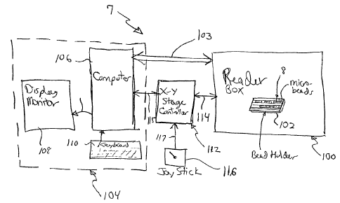
Referring to Fig. 1, an optical reader system 7 for diffraction grating based
encoded optical identification elements (such as microbeads), comprises a
reader box
100, which accepts a bead cell (or holder or cuvette or chamber) 102 that
holds and
aligns the microbeads 8 which have embedded codes therein. The reader box 100
interfaces along lines 103 with a known computer system 104 having a computer
106,
a display monitor 108, and a keyboard. In addition, the reader box 100
interfaces
along lines 114 with an stage position controller 112 and the controller 112
interfaces
along a line 115 with the computer system 104 and a manual control device (or
joy
stick) 116 along a line 117.
The microbeads 8 are similar to or the same as those described in pending US
Patent Application Serial No. 10/661,234 (CyVera Docket No. CV-0038A),
entitled
Diffraction Grating Based Optical Identification Element, filed Sept. 12,
2003, which
is incorporated herein by reference in its entirety, discussed more
hereinafter.
The bead cell 102 is similar to or the same as that described in pending US
Patent Application Serial No. 10/661,836 (CyVera Docket No. CV-0042), entitled
"Method and Apparatus for Aligning Microbeads in order to Interrogate the
same",
filed Sept. 12, 2003, as well as pending US Patent Applications, Serial Nos.
(CyVera
Docket Nos. CV-0054, CV-0082PR, CV-0086PR), which are all incorporated herein
by reference in its entirety, discussed more hereinafter.
- 12-
CA 02559801 2006-04-13
WO 2005/033681 PCT/US2004/032084
Referring to Fig. 2, the reader box 100 comprises the bead cell 102, certain
opto-mechanical elements 120 including a code camera, a edge trigger diode
which
measures a portion of the light reflected off the beads and provides signal
indicative
thereof to electronics discussed hereinafter, a green laser and red laser (for
fluorescence excitation, and code reading), 2 photo-multiplier tubes to detect
2
fluorescent signals from the beads, a laser power diode to detect and/or
calibrate laser
power, an alignment/imaging light to illuminate the bead holder and/or beads,
an
alignment/imaging vision camera to view an image of the bead holder and/or
beads,
laser control on/off shutter, stage mechanics to position the bead holder in
the desired
position for reading the beads, and various optics to cause the
excitation/read and
imaging optical signals to illuminate the beads and to allow the fluorescent
optical
signals, imaging optical signals, and code related optical signals to be read
by the
appropriate devices, as described herein.
In addition, the microbead reader system 7 includes various electronics 122 to
provide any needed interfacing/buffering between the PC and the external
devices and
to perform the various functions described herein, including a junction box
(optional)
for interfacing between the computer and the optomechanical parts, an edge
trigger
circuit which receives the signal from the edge trigger photodiode and
provides a
signal to the computer 104 indicative of when the incident light is incident
on an axial
end edge of a bead, laser control electronics to control the on/off solenoid
shutters 155
which control light from the green and red lasers, and photo-multiplier (PMT)
control
electronics to control the PMT's, e.g., to set the amount of gain on the PMTS.
Referring to Fig. 3, a block diagram of the opto-mechanical hardware 120
(Fig. 2) is shown. In particular, there are two excitation lasers, a green
laser 152, e.g.,
a diode pumped frequency doubled Nd:YAG laser that provides an output
wavelength
of about 532 nm (green) and has a beam waist of about O.Smm; and a red laser
150,
e.g., a red Helium Neon (HeNe) laser that provides an output wavelength of
about
633nm (red) and has a beam waist of about 0.3mm. Other beam sizes may be used
if
desired, provided it meets the performance/functions described herein for a
given
- 13-
CA 02559801 2006-04-13
WO 2005/033681 PCT/US2004/032084
application. The output signals are processed through optics 156,154,
respectively,
and passed to a polarization combiner 158 that combines both laser beams from
the
two lasers 150,152 into a single beam. Alternatively, the combiner 158 may be
a
wavelength combiner; however in that case, the laser power cannot be adjusted
by
polarization control. The single beam is then provided to mode matching optics
160
which creates a beam of the desired cross-sectional geometry (e.g.,
elliptical) to
illuminate the beads. The beam is also passed through various routing mirrors
162
(discussed hereinafter) which routes the beam to the desired location on the
bead
holder (or cuvette) 102. The bead holder is positioned in the desired position
to read a
given bead, by the mechanical X-Y translation stage 112. The beads provide two
optical signals, the first is a diffracted code optical signal, similar to
that discussed in
the aforementioned patent applications, which is passed to code pick-up optics
164
which routes the optical code signal to a code camera (or CCD camera) 168. The
second optical signal provided from the beads is a fluorescence signal, which
is
passed to fluorescence pickup optics and passed along a multimode optical
fiber 169,
e.g., Thor M2OL01, to PMT Receiver Module 170 which directs light from two
different wavelength fluorescent signals and provides each to a known
photodetector,
e.g., photomultiplier tubes (PMTS) discussed more hereinafter. Any
photodetector
having sufficient sensitivity may be used if desired. The PMTS provide a
signal to the
computer indicative of the fluorescence signal from the beads 8. Also, the
system may
have an alignment or imaging system 167 having an imaging camera for viewing
the
beads in the cell 102 or for alignment or other purposes (discussed
hereinafter).
Referring to Fig. 4, the laser block assembly comprises the lasers 150,152,
optics 154,156 and polarization beam combiner 158, are shown. In particular,
the
green laser 152, e.g., a 532 nm laser LCM-T-1 lccs, by Power Technology,
provides a
polarized optical laser signal to an on off Shutter 201. When the shutter 201
is
allowing light to pass, the light 203 is passed to a'/2 wave plate 200, e.g.,
CVI with a
D=l Omm, which may be rotated to adjust the power of the green laser 152. If
the laser
light provided by one or both of the lasers 150,152 is not polarized, optional
- 14-
CA 02559801 2006-04-13
WO 2005/033681 PCT/US2004/032084
polarizers 155,157 may be used to polarize the desired light and then passed
to the 1/2
wave plate. The wave plate 200 then provides polarization adjusted light to a
focusing lens 202, e.g., ~150mm PCX, D=25mm Edmond Indust. Optics, which
provides a converging or focussed beam 203 to a 532nm optical source filter
then to a
turning mirror 204. The distance between the green laser 152 and the wave
plate 200
is about 25mm. The distance between the lens 202 to the doublet lens 218 is
about
115 mm.
The mirror 204 may be adjustable about one or more pivot points to ensure
that the beam 203 is incident on the correct location. The green beam 203
converges
at a predetermined focal point Fee" 220. The distance between the lens 202 and
the
polarizing cube 158 may be adjusted t~ place a focal point Fgreen 220 for the
green
beam 203 at the desired focal location F~een. The mirror 204 directs the beam
203
onto the polarization combiner 158 (or cube).
The red laser 150, e.g., 633mn JDSU 1.5 mWatt laser, provides a polarized
optical laser light 213 to an on/off shutter 211. When the shutter 211 is
allowing light
to pass, the light 213 is passed to a %Z wave plate 210 (same as the waveplate
200)
which may be used to adjust the power of the red laser 150. The wave plate 210
then
provides polarization adjusted light to a focusing lens 212, e.g., ~75mm PCX
D=25mm lens from Edmond Indust. Optics, which provides a converging or
focussed
beam 213 to the polarization combiner 158 (or cube). The red beam 213
converges at
a predetermined focal point Frea 221 which is also an adjustable focal point
location
set at or near to the same location as the focal point Fg~en 220 for the green
beam 203.
The distance between the lens 212 and the polarizing cube 158 may be adjusted
to
place a red laser focal point Frea 221 for the red beam 213 at the desired
location. The
lens 212 is mounted to a Thor SPTl mount. The distance between the red laser
150
and the wave plate 210 is about 25mm. The distance between the lens 212 to the
doublet lens 218 is about 40 mm.
The shutters 201,211 are controlled such that when the green laser is
illuminating a given bead (for either code or fluorescence reading) the red
laser is not
- 15-
CA 02559801 2006-04-13
WO 2005/033681 PCT/US2004/032084
also illuminating that bead at the same time. The two lasers 150,152 may
illuminate
the same bead at the same time if desired, provided the fluorescent dyes used
with the
beads 8 are spectrally separated by a large enough wavelength space to allow
the
separate dyes to be detected.
The polarization beam combiner 158 combines the two beams 203,213 based
on their polarization and provides a combined beam 216, which is provided to a
doublet focusing lens 218, e.g., a 65 mm focal length doublet lens, which
works with
the focusing lenses 202, 212 to focus the combined beam 216 at a desired focal
point
220 as a focused beam 219. The beam combiner 158 provides the light beam 216
as a
circular beam and has a distance of about 610 rnm +/- 10 mm to the bead 8 (not
shown). The polarizing cube beam combiner 158 is mounted to a Thor Mount C4W.
Referring to Fig. 4a, alternatively, the laser block assembly 159 may comprise
an alternative configuration as shown. In particular, the green laser 152
provides the
light beams 304 to lens 300, e.g., a -50 mm F.L. lens Thor LD 1357, and then
to a
lens 302, e.g., a 50 mm FL lens Thor LB 1844, and then to a flip mirror 310.
When
the flip mirror 310 is in the up position, the light 304 passes to a lens 312
and to a
mirror 314 as a beam 306 to a lens 316 and to a turning mirror 318. The light
306 is
reflected off the turning mirror 318 and provided to a lens 319 and to a prism
315,
e.g., a lOmm, 45 degree prism Edmond Ind. Optics NT32-325, which redirects the
light 306 to a turning mirror 321 as the light beam 306. The lenses 316,319
are
cylindrical lenses, e.g., Edmond Ind. Optics, NT46-017. The light beam 306 is
used
for reading the code in the beads 8 as discussed herein and in the pending US
Patent
Applications referenced herein. The lenses 300,302 are used to accommodate or
compensate for beam tolerances in the green laser 152. When the flip mirror
310 is in
the down position, the light 304 reflects off the mirror 310 downward as a
light 308
which is incident on a beam combiner, e.g., Chromatic (or wavelength) Beam
Combiner Edmund Industries Optics, R47-265.
The red laser 150, e.g., a 635 nm Laser Sanyo DL-4148-21, provides a red
laser beam 324 to a lens 323, e.g., a 3.3 mm FL Lens Kodak A414TM. The light
324
- 16-
CA 02559801 2006-04-13
WO 2005/033681 PCT/US2004/032084
then passes through lenses 320,322, which may be the same type as the lenses
300,302, and are used to accommodate or compensate for beam tolerances in the
red
laser 150. The light 324 is incident on a compensating glass optic 332, e.g.,
Edmond
Ind. Optics, R47-265, which removes any astigmatism in the beam 324 that may
be
introduced by the chromatic beam combiner 334. The green light 308 and the red
light 324 are combined by the chromatic beam combiner 334 which provides a
combined beam 326 to a lens 328, e.g., a 25 mm FL lens Thor AC127-025. The
light
326 then passes to a turning mirror 330 and to a lens 336, e.g., a 75 mm FL
lens
Edmond Ind. Optics NT32-325. All the mirrors used in Fig. 4a are Edmond Ind.
Optics R43-790. The beam combiner 334 is also used to allow the red and green
beams to share the same path, even though they may not both be traveling along
that
path at the same time.
The shutters 303,323 are controlled such that when the green laser is
illuminating a given bead (for either code or fluorescence reading) the red
laser is not
1 S also illuminating that bead at the same time. The two lasers 150,152 may
illuminate
the same bead at the same time if desired, provided the fluorescent dyes used
with the
beads 8 are spectrally separated by a large enough wavelength space to allow
the
separate dyes to be detected.
Referring to Fig. 5, two side views of the combined beam 219 (from Fig. 4) is
shown as it would appear for light being incident on the end view (top portion
of Fig.
S) and side view (bottom portion of Fig. 5) of a bead 8. The combined beam 219
starting at the focal points Fg~een 220, Fred 221, passes through a first
cylindrical lens
222 and a second cylindrical lens 224 which creates a focused beam 228 to a
redirecting mirror 230 which is provided to the bead 8, having an elliptical
bead spot
geometry, with an end view 232 and a side view 234, designed to optimize the
ability
to read the bead code and the fluorescence with the same beam shape and
minimal
optical scatter. Such beam geometry is also discussed herein as well as in the
aforementioned patent application (CyVera Docket No. CV-0038A). The
cylindrical
lenses 222,224 may be a ~150mm cylindrical lens, 25 mm round; Edmunds E46-019.
- 17-
CA 02559801 2006-04-13
WO 2005/033681 PCT/US2004/032084
The focal point 221 lies along a virtual red point source plane 235 and the
green focal
point 220 lies along a virtual green point source plane 237. Also, the bead 8
is located
at the focal point of the beam 219, and lies in the image plane of the lens
system. The
distance from the virtual point source planes 235,237 to the first lens 222 is
about 235
mm, the distance from the virtual point source planes 235,237 to the second
lens 224
is about 415 mm, and the distance from the virtual point source planes 235,237
to the
bead 8 is about 650 mm. The two lenses 222,224 allow the beam 228
size/geometry to
be controlled independently in two different orthogonal optical axes. In
addition,
redirecting or routing or turning mirrors 234,236 may be placed between the
cylindrical lenses 222 to provide the desired beam path for the desired
mechanical
layout for the reader system 7 (also discussed hereinafter).
Referring to Figs. 5A & 5B, a single beam shape or multiple different beam
shapes may be used to read the code and fluorescence. In particular, in Fig.
5A, the
beam 228 has a spot geometry 240 on a top view of the bead 8 as an elliptical
shape,
which is used for both reading the code and reading the fluorescence of the
bead 8.
Wb= 15 microns for a 65 micron diameter bead (about 23% of the bead diameter
D),
and Lb= 200 microns for a 450 microns long bead (about 40% of the bead length
L).
One problem with this approach is that, for fluorescence measurement,
fluorescence
from an adjacent bead may bleed or cross over to the current bead being read,
thereby
providing inaccurate bead fluorescence readings for the bead.
Referring to Fig. 5B, we have found that the beam spot size and shape on the
bead 8 may be optimized to provide improved fluorescence and code measurements
by using a different shape beam for the code beam than that used for the
fluorescence
beam. In particular, we have found that for reading the code, an elliptical
beam shape
242 having a width Wb (1/e2 full width of beam) that is about the same as the
diameter D of the bead 8 and a beam length Lb that is about 45% of the bead
length L
provides good code read signals. The beam length Lb should not be so long as
to
cause the beam to scatter light off the edge of the bead being read into the
code
reading optics/camera; and do not want the beam length Lb too short or the
beam
- 18-
CA 02559801 2006-04-13
WO 2005/033681 PCT/US2004/032084
width Wb too narrow such that the bits cannot be resolved. The factors that
affect this
are as discussed in the aforementioned pending US patent application (Docket
No.
CV-0038A), which is incorporated herein by reference in its entirety.
Regarding fluorescence, we have found having a beam width Wb about equal
to the bead diameter D, provides the maximum amount of tolerance to variations
and
inaccuracies between the beam and bead position for reading the fluorescence
(i.e.,
transverse to the longitudinal axis of the bead), as discussed more
hereinafter. Also,
we have found that the beam length Lb should be about less than about 14 % of
the
bead length L to minimize bead edge effects and thus optimize reading
fluorescence
along the length of the bead 8, as discussed more hereinafter. Accordingly,
the beams
244, 246 may be circular, or elliptical provided the desired performance is
obtained.
For the red laser diode source discussed herein the red beam is not circular
and thus
the beam at the bead is not circular; however this could be corrected
optically if
desired. The beam shapes for fluorescence reading is described more
hereinafter.
Referring to Fig. 6, the combined excitation beam 228 is provided to the
routing mirror 230, e.g., 1"D x 3mmT ES 45-604, and directed to the bead 8
which
provides a transmitted beam 240 and a diffracted or reflected beam 242 from
the bead
code, as discussed in the aforementioned patent applications. The reflected
beam 242
is provided to a mirror 244, e.g,. 1"D x 3mmT ES 45-604, which provides the
light to
a bandpass filter 246, e.g., 532 nm BP filter ES NT47-136 (1" Diam), which is
adjacent to pair of lenses 247,249, e.g., each a ~100mm and each 25mm diam ES
32-
428. The bandpass filter 246 is designed to pass only the wavelength of light
associated with the excitation/source set for reading the code. This
substantially
eliminates the amount of optical noises/signal associated with other non-code
reading
wavelengths; thereby allowing a clean optical signal to pass to the code
camera 168.
The bandpass filter 246 provides filtered light 248 to a beamsplitter 250,
e.g., ES 43-
817 25mmxlmm R=25%, which reflects about 25% of the light along a path 252 to
the edge trigger photodiode 254, e.g., Sharp BS120 Digikey 425-1001-5-ND. The
diode 254 provides an electrical signal on a line 255 to the computer
indicative of the
- 19-
CA 02559801 2006-04-13
WO 2005/033681 PCT/US2004/032084
intensity of the light. The remainder of the input light 248 passes straight
through the
beamsplitter 250 as a beam 256 which creates a bead code image at a
predetermined
focal point 258. The lens pair around the bandpass filter 246 transfers the
image of the
reflected beam at the bead 8 to the bead code image point 258 as well as on
the edge
pick-up diode 254. The light 256 is provided to a video lens 260, e.g.,
Computar
V 1213 f =12.5, which provides a focused optical signal on the code camera
168, e.g.,
Lumera LU-OSOM. The video lens 260 is used as a Fourier lens to project the
Fourier
transform of the bead code from the point 258 onto the code camera 262. The
code
camera 262 provides a digital signal on a line 264 to the computer indicative
of the
bead code image at the point 258.
Referring to Fig. 6A, the BP filter 246 can be anywhere in the code path as
indicated by the numerals 261,263,265,267, provided it does not significantly
deteriorate wavefront performance of the optical system or degrade the lens
performance. The two ~100mm lenses 247,249 are for transferring the image from
the bead 8 to the intermediate point 258. Thus, the distance from the lens 249
to the
virtual image point 258 is 100mm and the distance from the bead 8 to the lens
247 is
about 100mm (equal to the focal length of the lenses 247, 249). Also, the
focal lengths
of the two lenses 247,249 need not be the same, provided appropriate distance
compensation is performed, and also depending on the application and
performance
specifications. Also, the distance from the point 258 to the video lens 260 is
about
l2.Smm and the distance from the video lens to the image plane on the camera
(and
the Fourier Plane) 269, is about l2.Smm (equal to the focal length of the
video lens
260). Technically, the lenses 247,249 should be separated by 2*f in order to
yield a
Fourier Transform at the image plane 269 of the code camera 168 (a typical 4f
system). However, this configuration does not cause the beam waist to change
substantially, thereby not significantly altering the performance of the
Fourier
transform. It should be understood that in Fig. 6A, the light travels from
left to right,
with connects with the prior optical drawing of Fig. 5. However, in the actual
-20-
CA 02559801 2006-04-13
WO 2005/033681 PCT/US2004/032084
hardware shown in the hardware Fig. 6, the bead 8 would be on the right side
and the
light would travel from right to left.
Referring to Fig. 6, the excitation beam 228 also excites fluorescent
molecules
attached to the bead 8, which provide a fluorescent optical signal 268 to a
fluorescence pick-up head 166, having a collimator, which directs the
fluorescent
optical signal into an optical fiber, e.g., a multimode optical fiber, which
is provided
to PMT optics, discussed hereinafter.
More specifically, referring to Fig. 6B, the fluorescent signal is provided to
a
collection objective lens 280, e.g., Lightpath (Geltech) 350220, F=l lmm
asphere
NA=0.25, which provides light to a long wavelength pass filter 282, e.g,. 0.5"
diam.
filter glass made by Schott Part No. 0G-570, to prevent excitation light at
532 nm
from getting into the fiber and causing the cladding to fluoresce. If the
fiber is made
of all glass, the filter is likely not needed. °The collection angle Oc
for light to enter the
fiber is set to about 30 degrees based on a predetermined numerical aperture
(NA).
Other values for the collection angle 8c may be used depending on the amount
of
stray light and the required detection performance. The light then passes to a
fiber
focusing assembly 284, e.g., Thor M15L01, which focuses the fluorescent light
268
into the end of the fiber 169. The collimator assembly 166 that may be used is
a Thor
F220-SMA-A Collimator.
In addition, when it is desired to view a visible image of the beads in the
bead
holder (e.g., for alignment, bead counting, or other purposes), a white LED
270, e.g,.
Lumex SSL-LX5093XUWC, is illuminated which provides a white light illumination
signal 272 up through the bottom of the bead holder and beads to illuminate
the beads
8. The LED 270 is mounted to a PMT shutter (discussed hereinafter) which
allows it
to flip out of the way when fluorescence is being detected. The illumination
image
signal 272 is provided to a mirror 274 which reflects the light 272 through a
first lens
279, e.g., Infinity 0.75x lens, and a second lens, e.g., Infinity 2x lens, and
then onto an
imaging/ vision camera 276, e.g., Lumera LU-OSOC. The vision camera 276
provides
-21-
CA 02559801 2006-04-13
WO 2005/033681 PCT/US2004/032084
an electrical signal on a line 278 to the computer indicative of the image
seen by the
imaging camera 276.
It should be understood that the alignment camera 276 may be on the same
side of the bead 8 (or bead holder 102) as the fluorescent pick-up 269.
Alternatively,
the location of the alignment camera 276 and fluorescent pick-up 269 may be
swapped, such that the alignment camera 276 is beneath the bead 8 and the pick-
up
269 is above the bead 8. It should be understood that one can swap the
incident beam
228 and the reflected beam 242 and the associated optics.
When the bead 8 is not present, the transmitted beam 240 may be incident on a
laser power diode 243, e.g., Hamamatsu 52307-16R, which provides an electrical
signal on a line 241 proportional to the power of the incident beam 228. This
may be
used for laser power calibration or other system calibration or test purposes.
This light
beam 228 may also be used for edge trigger information, as discussed
hereafter.
Referring to Fig. 7, the light from the fluorescent pick-up head 166 is
provided
along the fiber 169 e.g., Thor M20L01 multimode fiber, to a PMT receiver
module
170, which .includes a collimator assembly 281, e.g., Thor F230SMA-A, and a
focusing lens 282, e.g., f--100mm, 25mm diam. ES 32-482, which provides light
485
to a dichroic beam sputter 284, e.g., Omega 630 DLRP XF2021, 21x29mm, lmm
thick. The distance from the collimator assembly 281 to the beam splitter 284
is about
1 to 2 inches. The beam sputter 284 reflects light 286 of a first wavelength
(e.g., green
pumped Cy3 fluorescent light), and passes light 288 of a second wavelength
(e.g., red
pumped Cy5 fluorescent light). The light 286 is passed through an optical
aperture,
e.g., 12.5 mm Aperture Thor SM1A5, and then through an optical filter, e.g.,
Omega
3RD-570LP-610SP, 25 mm diam, about 3mm thick, that passes light of the first
wavelength (e.g., green pumped Cy3 fluorescent light), to a photomultiplier
tube
(PMT) 292, e.g., Hamamatsu H5783-20. The PMT 292 detects the intensity of the
incident fluorescent light and provides an output electrical signal on a line
293 to the
computer indicative of the intensity of the fluorescence signal incident on
the PMT
292.
-22-
CA 02559801 2006-04-13
WO 2005/033681 PCT/US2004/032084
Similarly, the light 288 passes through an optical aperture, e.g., 12.5 mm
Aperture Thor SM1A5, and then through a filter glass RG645, 1" diam, lmm thick
and then through an optical filter, e.g., Omega 695AF55, XF3076, 25 mm diam,
about
3mm thick, that passes light of the second wavelength (e.g., red pumped Cy5
fluorescent light), to a second photomultiplier tube (PMT) 296, e.g.,
Hamamatsu
H5783-20. The PMT 296 detects the intensity of the incident fluorescent light
and
provides an output electrical signal on a line 293 to the computer indicative
of the
intensity of the fluorescence signal incident on the PMT 296.
It should be understood that fluorescent molecules that are excited by the 532
nm (green) laser produce a fluorescent signal having a wavelength of about 570
nm
(orange color), and fluorescent molecules that are excited by the 633 nm (red)
laser
produce a fluorescent signal having a wavelength of about 670 nm (deep red
color).
Accordingly, the fluorescent signal on the line 286 will have an orange color
and the
light 288 will be deep red.
Referring to Figs. 8-22, show various perspective and cutaway views of the
present invention. It also shows the path of the light beams from various
views.
Referring to Figs. 8-10, perspective views of one embodiment of the present
invention, which shows numerous parts having the same numerals as in other
Figs.
herein, and also shows, a green laser power supply and control 402, red laser
power
supply and control 406, a frame or housing 410, and a main circuit board 410.
Fig. 12
is a physical drawing of one embodiment of Fig. 4 laser block assembly.
The parts used for the present invention are known parts and may be
substituted for other parts that provide the same function as that described
herein,
unless stated otherwise.
For example, as discussed herein, the code camera may be a USB 2.0 camera,
comprising a Luminera Monochromatic camera; part no. LU-OSOM, coupled to a
Computar 12.5 mm focal length TV lens. The camera provides a USB 2.0
(universal
serial bus) serial data stream indicative of the image seen by the camera.
Alternatively, the camera may be a standard CCD camara, or a CCD linear array,
part
-23-
CA 02559801 2006-04-13
WO 2005/033681 PCT/US2004/032084
No. CCD 111 made by Fairchild Imaging Corp., or other camera capable of
providing
a digital or analog signal indicative of the image seen, having sufficient
resolution to
identify the bits in the code in the beads 8. In that case, a "frame grabber"
and A/D
converter may be needed within the computer to properly condition the code
signal
S for processing. In addition, the camera accepts a trigger signal to command
the
camera to capture or save or transmit the image seen by the camera. The image
or
vision camera may be a Luminera LU-OSOC, USB 2.0 color camera. The X-Y
translation stage may be a Ludl X-Y precision stage driver/controller, having
motor
drives, position feedback and limit signals. Any other x-y stage may be used
if
desired, provided the stage can be positioned with sufficient accuracy to
accurately
read the beads 8.
The adjustable focus lenses described herein allow the setting of the spot
size
and focal point for the green and red laser light. One embodiment of the
system
described herein has three shutters that are controlled by the computer, one
for each
laser and one to prevent light from getting to the PMTs. This shutter also
holds the
white light source discussed herein for the bead Imaging System.
Referring to Fig. 23, a diffraction grating-based optical identification
element
8 (or encoded element or coded element) comprises a known optical substrate
10,
having an optical diffraction grating 12 disposed (or written, impressed,
embedded,
imprinted, etched, grown, deposited or otherwise formed) in the volume of or
on a
surface of a substrate 10. The grating 12 is a periodic or aperiodic variation
in the
effective refractive index and/or effective optical absorption of at least a
portion of the
substrate 10.
The optical identification element described herein is the same as that
described in Copending Patent Application Serial No. (CiDRA Docket No. CC-
0648A), filed contemporaneously herewith, which is incorporated herein by
reference
in its entirety.
In particular, the substrate 10 has an inner region 20 where the grating 12 is
located. The inner region 20 may be photosensitive to allow the writing or
impressing
-24-
CA 02559801 2006-04-13
WO 2005/033681 PCT/US2004/032084
of the grating 12. The substrate 10 has an outer region 18 which does not have
the
grating 12 therein.
The grating 12 is a combination of one or more individual spatial periodic
sinusoidal variations (or components) in the refractive index that are
collocated at
substantially the same location on the substrate 10 along the length of the
grating
region 20, each having a spatial period (or pitch) A. The resultant
combination of
these individual pitches is the grating 12, comprising spatial periods (Al-An)
each
representing a bit in the code. Thus, the grating 12 represents a unique
optically
readable code, made up of bits, where a bit corresponds to a unique pitch A
within the
grating 12. Accordingly, for a digital binary (0-1) code, the code is
determined by
which spatial periods (Al-An) exist (or do not exist) in a given composite
grating 12.
The code or bits may also be determined by additional parameters (or
additional
degrees of multiplexing), and other numerical bases for the code may be used,
as
discussed herein and/or in the aforementioned patent application.
The grating 12 may also be referred to herein as a composite or collocated
grating. Also, the grating 12 may be referred to as a "hologram", as the
grating 12
transforms, translates, or filters an input optical signal to a predetermined
desired
optical output pattern or signal.
The substrate 10 has an outer diameter D1 and comprises silica glass (Si02)
having the appropriate chemical composition to allow the grating 12 to be
disposed
therein or thereon. Other materials for the optical substrate 10 may be used
if desired.
For example, the substrate 10 may be made of any glass, e.g., silica,
phosphate glass,
borosilicate glass, or other glasses, or made of glass and a polymer, or
solely a
polymer. For high temperature or harsh chemical applications, the optical
substrate
10 made of a glass material is desirable. If a flexible substrate is needed,
plastic,
rubber or polymer-based substrate may be used. The optical substrate 10 may be
any
material capable of having the grating 12 disposed in the grating region 20
and that
allows light to pass through it to allow the code to be optically read.
-25-
CA 02559801 2006-04-13
WO 2005/033681 PCT/US2004/032084
The optical substrate 10 with the grating 12 has a length L and an outer
diameter D1, and the inner region 20 diameter D. The length L can range from
very
small "microbeads" (or microelements, micro-particles, or encoded particles),
about
1-1000 microns or smaller, to larger "macroelements" for larger applications
(about
1.0 - 1000 mm or greater). In addition, the outer dimension D1 can range from
small
(less than 1000 microns) to large (1.0 -1000 mm and greater). Other dimensions
and
lengths for the substrate 10 and the grating 12 may be used.
The optical substrate 10 with the grating 12 has a length L and an outer
diameter Dl, and the inner region 20 diameter D. The length L can range from
very
small (about 1-1000 microns or smaller) to large (about 1.0 - 1000 mm or
greater). In
addition, the outer dimension D1 can range from small (less than 1000 microns)
to
large (1.0 - 1000 mm and greater). Other dimensions and lengths for the
substrate 10
and the grating 12 may be used. Also, the element may be embedded within or
part of
a larger substrate or object. The element may also be in the form of a thread
or fiber to
be weaved into a material.
Some non-limiting examples of microbeads discussed herein are about 28
microns diameter and about 250 microns long, and about 65 microns diameter and
about 400 microns long. Other lengths may be used as discussed herein.
The grating 12 may have a length Lg of about the length L of the substrate 10.
Alternatively, the length Lg of the grating 12 may be shorter than the total
length L of
the substrate 10.
The outer region 18 is made of pure silica (Si02) and has a refractive index
n2
of about 1.458 (at a wavelength of about 1553 nm), and the inner grating
region 20 of
the substrate 10 has dopants, such as germanium andlor boron, to provide a
refractive
index n1 of about 1.453, which is less than that of outer region 18 by about
0.005.
Other indices of refraction nl,n2 for the grating region 20 and the outer
region 18,
respectively, may be used, if desired, provided the grating 12 can be
impressed in the
desired grating region 20. For example, the grating region 20 may have an
index of
-26-
CA 02559801 2006-04-13
WO 2005/033681 PCT/US2004/032084
refraction that is larger than that of the outer region 18 or grating region
20 may have
the same index of refraction as the outer region 18 if desired.
Referring to Fig. 24, an incident light 24 of a wavelength ~,, e.g., 532 nm
from
a known frequency doubled Nd:YAG laser or 632nm from a known Helium-Neon
laser, is incident on the grating 12 in the substrate 10. Any other input
wavelength ~,
can be used if desired provided ~, is within the optical transmission range of
the
substrate (discussed more herein and/or in the aforementioned patent
application). A
portion of the input light 24 passes straight through the grating 12, as
indicated by a
line 25. The remainder of the input light 24 is reflected by the grating 12,
as indicated
by a line 27 and provided to a detector 29. The output light 27 may be a
plurality of
beams, each having the same wavelength ~, as the input wavelength ~, and each
having
a different output angle indicative of the pitches (Al-An) existing in the
grating 12.
Alternatively, the input light 24 may be a plurality of wavelengths and the
output light
27 may have a plurality of wavelengths indicative of the pitches (A1-An)
existing in
the grating 12. Alternatively, the output light may be a combination of
wavelengths
and output angles. The above techniques are discussed in more detail herein
and/or in
the aforementioned patent application.
The detector 29 has the necessary optics, electronics, software and/or
firmware
to perform the functions described herein. In particular, the detector reads
the optical
signal 27 diffracted or reflected from the grating 12 and determines the code
based on
the pitches present or the optical pattern, as discussed more herein or in the
aforementioned patent application. An output signal indicative of the code is
provided
on a line 31.
Referring to Fig. 25, The reflected light 27, comprises a plurality of beams
26-
36 that pass through a lens 37, which provides focused light beams 46-56,
respectively, which are imaged onto a CCD camera 60. The lens 37 and the
camera
60, and any other necessary electronics or optics for performing the functions
described herein, make up the reader 29. Instead of or in addition to the lens
37, other
imaging optics may be used to provide the desired characteristics of the
optical
- 27 -
CA 02559801 2006-04-13
WO 2005/033681 PCT/US2004/032084
image/signal onto the camera 60 (e.g., spots, lines, circles, ovals, etc.),
depending on
the shape of the substrate 10 and input optical signals. Also, instead of a
CCD camera
other devices may be used to read/capture the output light.
Referring to Fig. 26, the image on the CCD camera 60 is a series of
illuminated stripes indicating ones and zeros of a digital pattern or code of
the grating
12 in the element 8. Referring to Fig. 27, lines 68 on a graph 70 are
indicative of a
digitized version of the image of Fig. 26 as indicated in spatial periods (A1-
An).
Each of the individual spatial periods (A1-An) in the grating 12 is slightly
different, thus producing an array of N unique diffraction conditions (or
diffraction
angles) discussed more hereinafter. When the element 8 is illuminated from the
side,
in the region of the grating 12, at an appropriate input angle, e.g., about 30
degrees,
with a single input wavelength ~, (monochromatic) source, the diffracted (or
reflected)
beams 26-36 are generated. Other input angles 8i may be used if desired,
depending
on various design parameters as discussed herein and/or in the aforementioned
patent
application, and provided that a known diffraction equation (Eq. 1 below) is
satisfied:
sin(~; ) + sin(~a ) = m~, / ~cA Eq. 1
where Eq. 1 is diffraction (or reflection or scatter) relationship between
input
wavelength ~., input incident angle 8i, output incident angle 00, and the
spatial period
A of the grating 12. Further, m is the "order" of the reflection being
observed, and n is
the refractive index of the substrate 10. The value of m=1 or first order
reflection is
acceptable for illustrative purposes. Eq. 1 applies to light incident on outer
surfaces of
the substrate 10 which are parallel to the longitudinal axis of the grating
(or the k$
vector). Because the angles 6i,0o are defined outside the substrate 10 and
because the
effective refractive index of the substrate 10 is substantially a common
value, the
value of n in Eq. 1 cancels out of this equation.
Thus, for a given input wavelength 7~, grating spacing A, and incident angle
of
the input light 8i, the angle 00 of the reflected output light may be
determined.
Solving Eq. 1 for 8o and plugging in m=1, gives:
-28-
CA 02559801 2006-04-13
WO 2005/033681 PCT/US2004/032084
0 0 = sih 1 (alA - sin(8 i)) Eq. 2
For example, for an input wavelength ~, = 532 nm, a grating spacing A= 0.532
microns (or 532 nm), and an input angle of incidence 8i =30 degrees, the
output angle
of reflection will be 00 = 30 degrees. Alternatively, for an input wavelength
~, = 632
S nm, a grating spacing A = 0.532 microns (or 532 nm), and an input angle 8i
of 30
degrees, the output angle of reflection 0o will be at 43.47 degrees, or for an
input
angle 8i = 37 degrees, the output angle of reflection will be 00 = 37 degrees.
Any
input angle that satisfies the design requirements discussed herein and/or in
the
aforementioned patent application may be used.
In addition, to have sufficient optical output power and signal to noise
ratio,
the output light 27 should fall within an acceptable portion of the Bragg
envelope (or
normalized reflection efficiency envelope) curve 200, as indicated by points
204,206,
also defined as a Bragg envelope angle 8B, as also discussed herein and/or in
the
aforementioned patent application. The curve 200 may be defined as:
I (ki, ko) ~ ~KD~2 sin c2 (ki - ko)D E . 3
2 ~ q
where K = 2~8n/7~, where, 8n is the local refractive index modulation
amplitude of the
grating and 7~ is the input wavelength, sinc(x) = sin(x)/x, and the vectors k;
_
2~ccos(0;)/~, and ko= 2~cos (60)/x, are the projections of the incident light
and the
output (or reflected) light, respectively, onto the line 203 normal to the
axial direction
of the grating 12 (or the grating vector k$), D is the thickness or depth of
the grating
12 as measured along the line 203 (normal to the axial direction of the
grating 12).
Qther substrate shapes than a cylinder may be used and will exhibit a similar
peaked
characteristic of the Bragg envelope. We have found that a value for 8n of
about 10'~
in the grating region of the substrate is acceptable; however; other values
may be used
if desired.
Rewriting Eq. 3 gives the reflection efficiency profile of the Bragg envelope
as:
-29-
CA 02559801 2006-04-13
WO 2005/033681 PCT/US2004/032084
I(ki, ko) ~ ~2~ ~ ~ ~ D~ZCSin(x)12 Eq. 4
Jx
where: x =(ki-ko)Dl2 = (~Dla,) *(cos9 i - cos A o)
Thus, when the input angle 0i is equal to the output (or reflected) angle 80
(i.e., 8i = 60), the reflection efficiency I (Eqs. 3 & 4) is maximized, which
is at the
center or peak of the Bragg envelope. When 8i = Oo, the input light angle is
referred
to as the Bragg angle as is known. The efficiency decreases for other input
and output
angles (i.e., Ai ~ 60), as defined by Eqs. 3 & 4. Thus, for maximum reflection
efficiency and thus output light power, for a given grating pitch A and input
wavelength, the angle Ai of the input light 24 should be set so that the angle
Ao of the
reflected output light equals the input angle Oi.
Also, as the thickness or diameter D of the grating decreases, the width of
the
sin(x)/x function (and thus the width of the Bragg envelope) increases and,
the
coefficient to or amplitude of the since (or (sin(x)/x) ~ function (and thus
the efficiency
level across the Bragg envelope) also increases, and vice versa. Further, as
the
wavelength ~, increases, the half width of the Bragg envelope as well as the
efficiency
level across the Bragg envelope both decrease. Thus, there is a trade-off
between the
brightness of an individual bit and the number of bits available under the
Bragg
envelope. Ideally, 8n should be made as large as possible to maximize the
brightness,
which allows D to be made smaller.
From Eq. 3 and 4, the half angle of the Bragg envelope 6B is defined as:
__
~zl~ sin(~ ~ ) ~ Eq. 5
where ~ is a reflection efficiency factor which is the value for x in the
sinc2(x)
function where the value of sinc2(x) has decreased to a predetermined value
from the
maximum amplitude as indicated by points 204,206 on the curve 200.
We have found that the reflection efficiency is acceptable when r1 < 1.39.
This
value for r1 corresponds to when the amplitude of the reflected beam (i.e.,
from the
- 30 -
CA 02559801 2006-04-13
WO 2005/033681 PCT/US2004/032084
sinc2(x) function of Eqs. 3 & 4) has decayed to about 50% of its peak value.
In
particular, when x = 1.39 = r1, sinc2(x) = 0.5. However, other values for
efficiency
thresholds or factor in the Bragg envelope may be used if desired.
The beams 26-36 are imaged onto the CCD camera 60 to produce the pattern
of light and dark regions 120-132 representing a digital (or binary) code,
where light
=1 and dark = 0 (or vice versa). The digital code may be generated by
selectively
creating individual index variations (or individual gratings) with the desired
spatial
periods Al-An. Other illumination, readout techniques, types of gratings,
geometries,
materials, etc. may be used as discussed in the aforementioned patent
application.
Referring to Fig. 28, illustrations (a)-(c), for the grating 12 in a
cylindrical
substrate 10 having a sample spectral 17 bit code (i.e., 17 different pitches
Al-A17),
the corresponding image on the CCD (Charge Coupled Device) camera 60 is shown
for a digital pattern of 7 bits turned on (10110010001001001); 9 bits turned
on of
(11000101010100111); all 17 bits turned on of (11111111111111111).
For the images in Fig. 28, the length of the substrate 10 was 450 microns, the
outer diameter D1 was 65 microns, the inner diameter D was 14 microns, 8n for
the
grating 12 was about 10~, n1 in portion 20 was about 1.458 (at a wavelength of
about
1550 nm), n2 in portion 18 was about 1.453, the average pitch spacing A for
the
grating 12 was about 0.542 microns, and the spacing between pitches ~A was
about
0.36 % of the adjacent pitches A.
Referring to Fig. 29, illustration (a), the pitch A of an individual grating
is the
axial spatial period of the sinusoidal variation in the refractive index n1 in
the region
20 of the substrate 10 along the axial length of the grating 12 as indicated
by a curve
90 on a graph 91. Referring to Fig. 29, illustration (b), a sample composite
grating 12
comprises three individual gratings that are co-located on the substrate 10,
each
individual grating having slightly different pitches, Al, A2, A3,
respectively, and the
difference (or spacing) DA between each pitch A being about 3.0 % of the
period of
an adjacent pitch A as indicated by a series of curves 92 on a graph 94.
Referring to
-31-
CA 02559801 2006-04-13
WO 2005/033681 PCT/US2004/032084
Fig. 29, illustration (c), three individual gratings, each having slightly
different
pitches, Al, A2, A3, respectively, are shown, the difference ~A between each
pitch A
being about 0.3% of the pitch A of the adjacent pitch as shown by a series of
curves
95 on a graph 97. The individual gratings in Fig. 29, illustrations (b) and
(c) are
shown to all start at 0 for illustration purposes; however, it should be
understood that,
the separate gratings need not all start in phase with each other. Referring
to Fig. 29,
illustration (d), the overlapping of the individual sinusoidal refractive
index variation
pitches A1-An in the grating region 20 of the substrate 10, produces a
combined
resultant refractive index variation in the composite grating 12 shown as a
curve 96 on
a graph 98 representing the combination of the three pitches shown in Fig. 29,
illustration (b). Accordingly, the resultant refractive index variation in the
grating
region 20 of the substrate 10 may not be sinusoidal and is a combination of
the
individual pitches A (or index variation).
The maximum number of resolvable bits N, which is equal to the number of
different grating pitches A (and hence the number of codes), that can be
accurately
read (or resolved) using side-illumination and side-reading of the grating 12
in the
substrate 10, is determined by numerous factors, including: the beam width w
incident
on the substrate (and the corresponding substrate length L and grating length
Lg), the
thickness or diameter D of the grating 12, the wavelength ~, of incident
light, the beam
divergence angle OR, and the width of the Bragg envelope 6B (discussed more in
the
aforementioned patent application), and may be determined by the equation:
_ ~7,QL q
2Dsin(0;) E .6
Referring to 30, illustration (b), the transmission wavelength spectrum of the
transmitted output beam 330 (which is transmitted straight through the grating
12)
will exhibit a series of notches (or dark spots) 696. Alternatively, instead
of detecting
the reflected output light 310, the transmitted light 330 may be detected at
the
detector/reader 308. It should be understood that the optical signal levels
for the
- 32 -
CA 02559801 2006-04-13
WO 2005/033681 PCT/US2004/032084
reflection peaks 695 and transmission notches 696 will depend on the
"strength" of
the grating 12, i.e., the magnitude of the index variation n in the grating
12.
Referring to Fig. 31, instead of or in addition to the pitches A in the
grating 12
being oriented normal to the longitudinal axis, the pitches may be created at
a angle
0g. In that case, when the input light 24 is incident normal to the surface
792, will
produce a reflected output beam 790 having an angle 0o determined by Eq. 1 as
adjusted for the blaze angle 0g. This can provide another level of
multiplexing bits in
the code.
The grating 12 may be impressed in the substrate 10 by any technique for
writing, impressed, embedded, imprinted, or otherwise forming a diffraction
grating
in the volume of or on a surface of a substrate 10. Examples of some known
techniques are described in US Patent No. 4,725,110 and 4,807,950, entitled
"Method
for Impressing Gratings Within Fiber Optics", to Glenn et al; and US Patent
No.
5,388,173, entitled "Method and Apparatus for Forming Aperiodic Gratings in
Optical Fibers", to Glenn, respectively, and US Patent 5,367,588, entitled
"Method of
Fabricating Bragg Gratings Using a Silica Glass Phase Grating Mask and Mask
Used
by Same", to Hill, and US Patents 3,916,182, entitled "Periodic Dielectric
Waveguide
Filter", Dabby et al, and US Patent 3,891,302, entitled "Method of Filtering
Modes in
Optical Waveguides", to Dabby et al, which are all incorporated herein by
reference
to the extent necessary to understand the present invention.
Alternatively, instead of the grating 12 being impressed within the substrate
material, the grating 12 may be partially or totally created by etching or
otherwise
altering the outer surface geometry of the substrate to create a corrugated or
varying
surface geometry of the substrate, such as is described in US Patent
3,891,302,
entitled "Method of Filtering Modes in Optical Waveguides", to Dabby et al,
which is
incorporated herein by reference to the extent necessary to understand the
present
invention, provided the resultant optical refractive profile for the desired
code is
created.
-33-
CA 02559801 2006-04-13
WO 2005/033681 PCT/US2004/032084
Further, alternatively, the grating 12 may be made by depositing dielectric
layers onto the substrate, similar to the way a known thin film filter is
created, so as to
create the desired resultant optical refractive profile for the desired code.
The substrate 10 (and/or the element 8) may have end-view cross-sectional
shapes other than circular, such as square, rectangular, elliptical, clam-
shell, D-
shaped, or other shapes, and may have side-view sectional shapes other than
rectangular, such as circular, square, elliptical, clam-shell, D-shaped, or
other shapes.
Also, 3D geometries other than a cylinder may be used, such as a sphere, a
cube, a
pyramid or any other 3D shape. Alternatively, the substrate 10 may have a
geometry
that is a combination of one or more of the foregoing shapes.
The shape of the element 8 and the size of the incident beam may be made to
minimize any end scatter off the end faces) of the element 8, as is discussed
herein
and/or in the aforementioned patent application. Accordingly, to minimize such
scatter, the incident beam 24 may be oval shaped where the narrow portion of
the oval
is smaller than the diameter D1, and the long portion of the oval is smaller
than the
length L of the element 8. Alternatively, the shape of the end faces may be
rounded or
other shapes or may be coated with an antireflective coating.
It should be understood that the size of any given dimension for the region 20
of the grating 12 may be less than any corresponding dimension of the
substrate 10.
For example, if the grating 12 has dimensions of length Lg, depth Dg, and
width Wg,
and the substrate 12 has different dimensions of length L, depth D, and width
W, the
dimensions of the grating 12 may be less than that of the substrate 12. Thus,
the
grating 12, may be embedded within or part of a much larger substrate 12.
Also, the
element 8 may be embedded or formed in or on a larger object for
identification of the
object.
The dimensions, geometries, materials, and material properties of the
substrate
10 are selected such that the desired optical and material properties are met
for a
given application. The resolution and range for the optical codes are scalable
by
- 34 -
CA 02559801 2006-04-13
WO 2005/033681 PCT/US2004/032084
controlling these parameters as discussed herein and/or in the aforementioned
patent
application.
Referring to Fig. 32, the substrate 10 may have an outer coating 799, such as
a
polymer or other material that may be dissimilar to the material of the
substrate 10,
provided that the coating 799 on at least a portion of the substrate, allows
sufficient
light to pass through the substrate for adequate optical detection of the
code. The
coating 799 may be on any one or more sides of the substrate 10. Also, the
coating
799 may be a material that causes the element 8 to float or sink in certain
fluids
(liquid and/or gas) solutions.
Also, the substrate 10 may be made of a material that is less dense than
certain
fluid (liquids and/or gas) solutions, thereby allowing the elements 8 to float
or be
buoyant or partially buoyant. Also, the substrate may be made of a porous
material,
such as controlled pore glass (CPG) or other porous material, which may also
reduce
the density of the element 8 and may make the element 8 buoyant or partially-
buoyant
in certain fluids.
Also, the grating 12 is axially spatially invariant. As a result, the
substrate 10
with the grating 12 may be axially subdivided or cut into many separate
smaller
substrates and each substrate will contain the same code as the longer
substrate had
before it was cut. The limit on the size of the smaller substrates is based on
design and
~ performance factors discussed herein and/or in.the aforementioned patent
application. .
Referring to Fig. 33, one purpose of the outer region 18 (or region without
the
grating 12) of the substrate 10 is to provide mechanical or structural support
for the
inner grating region 20. Accordingly, the entire substrate 10 may comprise the
grating
12, if desired. Alternatively, the support portion may be completely or
partially
beneath, above, or along one or more sides of the grating region 20, such as
in a
planar geometry, or a D-shaped geometry, or other geometries, as described
herein
and/or in the aforementioned patent application. The non-grating portion 18 of
the
substrate 10 may be used for other purposes as well, such as optical Tensing
effects or
other effects (discussed herein or in the aforementioned patent application).
Also, the
-35-
CA 02559801 2006-04-13
WO 2005/033681 PCT/US2004/032084
end faces of the substrate 10 need not be perpendicular to the sides or
parallel to each
other. However, for applications where the elements 8 are stacked end-to-end,
the
packing density may be optimized if the end faces are perpendicular to the
sides.
Referring to Figs. 34, illustrations (a)-(c), two or more substrates 10,250,
each
having at least one grating therein, may be attached together to form the
element 8,
e.g., by an adhesive, fusing or other attachment techniques. In that case, the
gratings
12,252 may have the same or different codes.
Referring to Figs. 35, illustrations (a) and (b), the substrate 10 may have
multiple regions 80,90 and one or more of these regions may have gratings in
them.
For example, there may be gratings 12,252 side-by-side (illustration (a)), or
there may
be gratings 82-88, spaced end-to-end (illustration (b)) in the substrate 10.
Referring to Fig. 36, the length L of the element 8 may be shorter than its
diameter D, thus, having a geometry such as a plug, puck, wafer, disc or
plate.
Referring to Fig. 37, to facilitate proper alignment of the grating axis with
the
angle 8i of the input beam 24, the substrate 10 may have a plurality of the
gratings 12
having the same codes written therein at numerous different angular or
rotational (or
azimuthal) positions of the substrate 10. In particular, two gratings 550,
552, having
axial grating axes 551, 553, respectively may have a common central (or pivot
or
rotational) point where the two axes 551,553 intersect. The angle Oi of the
incident
light 24 is aligned properly with the grating 550 and is not aligned with the
grating
552, such that output light 555 is reflected off the grating 550 and light 557
passes
through the grating S50 as discussed herein. If the element 8 is rotated as
shown by
the arrows 559, the angle Ai of incident light 24 will become aligned properly
with the
grating 552 and not aligned with the grating 550 such that output light 555 is
reflected
off the grating 552 and light 557 passes through the grating 552. When
multiple
gratings are located in this rotational orientation, the bead may be rotated
as indicated
by a line 559 and there may be many angular positions that will provide
correct (or
optimal) incident input angles Oi to the grating. While this example shows a
circular
cross-section, this technique may be used with any shape cross-section.
-36-
CA 02559801 2006-04-13
WO 2005/033681 PCT/US2004/032084
Referring to Fig. 38, illustrations (a), (b), (c), (d), and (e) the substrate
10 may
have one or more holes located within the substrate 10. In illustration (a),
holes 560
may be located at various points along all or a portion of the length of the
substrate
10. The holes need not pass all the way through the substrate 10. Any number,
size
and spacing for the holes 560 may be used if desired. In illustration (b),
holes 572
may be located very close together to form a honeycomb-like area of all or a
portion
of the cross-section. In illustration (c), one (or more) inner hole 566 may be
located in
the center of the substrate 10 or anywhere inside of where the grating
regions) 20 are
located. The inner hole 566 may be coated with a reflective coating 573 to
reflect light
to facilitate reading of one or more of the gratings 12 and/or to reflect
light diffracted
off one or more of the gratings 12. The incident light 24 may reflect off the
grating 12
in the region 20 and then reflect off the surface 573 to provide output light
577.
Alternatively, the incident light 24 may reflect off the surface 573, then
reflect off the
grating 12 and provide the output_light 575. In that case the grating region
20 may run
axially or circumferentially 571 around the substrate 10. In illustration (d),
the holes
579 may be located circumferentially around the grating region 20 or
transversely
across the substrate 10. In illustration (e), the grating 12 may be located
circumferentially around the outside of the substrate 10, and there may be
holes 574
inside the substrate 10.
- Referring to Fig. 39, illustrations (a), (b), and (c), the substrate 10 may
have
one or more protruding portions or teeth 570, 578,580 extending radially
and/or
circumferentially from the substrate 10. Alternatively, the teeth 570, 578,580
may
have any other desired shape.
Referring to Fig. 40, illustrations (a), (b), (c) a D-shaped substrate, a flat-
sided
substrate and an eye-shaped (or clam-shell or teardrop shaped) substrate 10,
respectively, are shown. Also, the grating region 20 may have end cross-
sectional
shapes other than circular and may have side cross-sectional shapes other than
rectangular, such as any of the geometries described herein for the substrate
10. For
example, the grating region 20 may have a oval cross-sectional shape as shown
by
- 37 -
CA 02559801 2006-04-13
WO 2005/033681 PCT/US2004/032084
dashed lines 581, which may be oriented in a desired direction, consistent
with the
teachings herein. Any other geometries for the substrate 10 or the grating
region 20
may be used if desired, as described herein.
Referring to Fig. 41, at least a portion of a side of the substrate 10 may be
coated with a reflective coating to allow incident light S 10 to be reflected
back to the
same side from which the incident light came, as indicated by reflected light
S 12.
Referring to Fig. 42, illustrations (a) and (b), alternatively, the substrate
10 can
be electrically and/or magnetically polarized, by a dopant or coating, which
may be
used to ease handling and/or alignment or orientation of the substrate 10
and/or the
grating 12, or used for other purposes. Alternatively, the bead may be coated
with
conductive material, e.g., metal coating on the inside of a holy substrate, or
metallic
dopant inside the substrate. In these cases, such materials can cause the
substrate 10 to
align in an electric or magnetic field. Alternatively, the substrate can be
doped with an
element or compound that fluoresces or glows under appropriate illumination,
e.g., a
rare earth dopant, such as Erbium, or other rare earth dopant or fluorescent
or
luminescent molecule. In that case, such fluorescence or luminescence may
aid.in
locating and/or aligning substrates.
Unless otherwise specifically stated herein, the term "microbead" is used
herein as a label and does not restrict any embodiment or application of the
present
invention to certain dimensions, materials .and/or geometries.
Referring to Fig. 43, the codes that are on the beads may be indicative of any
type of desired information such as that described in U.S. Patent Application
Serial
No. 10/661,082 (Docket No. CV-0040), filed September 12, 2003, entitled
"Method
and Apparatus for Labeling Using Diffraction Grating-Based Encoded Optical
Identification Elements". For example, in Fig. 43, the code may be a simple
code or
may be a more complex code having many pieces of information located in the
code.
In addition, the code may have checks within the code to ensure the code is
read
correctly. It can be viewed as a serial digital message, word, or frame
consisting of N
bits.
-38-
CA 02559801 2006-04-13
WO 2005/033681 PCT/US2004/032084
In particular, there may be start and stop bits 869, 871, respectively. The
start
and stop bits may each take up more than one bit location if desired. In
addition, there
may be an error check portion of the message, such as a check sum or CRC
(cyclic
redundancy check) having a predetermined number of bits, and a code section
873
having a predetermined number of bits. The error check portion ensures that
the code
which is obtained from the bead is accurate. Accordingly, having a large
number of
bits in the element 8 allows for greater statistical accuracy in the code
readout and
decreases the likelihood of providing an erroneous code. Accordingly, if a
code
cannot be read without an error, no code will be provided, avoiding an
erroneous
result. Any known techniques for digital error checking for single or mufti-
bit errors
may be used.
The code section 873 may be broken up into one or more groups of bits, for
example, three bit groups 863,865,867, each bit group containing information
about
the bead.itself or the item attached to the bead or how the bead is to be
used, or other
. information. For example, the first bit group 863 may contain information
regarding
"identifying numbers", such as: lot number, quality control number, model
number,
serial number, inventory control number; the second bit group 865 may contain
"type" information, such as: chemical or cell type, experiment type, item
type, animal
type; and the third bit group 867 may contain "date" information, such as:
manufactured date, experiment date, creation date, initial tracking date. Any
other bit
groups, number of bit groups, or size of bit groups may be used if desired.
Also,
additional error or fault checking can be used if desired.
In particular, for a product manufacturing application, the code may have the
serial number, the lot number, date of manufacture, etc. or have other
information that
identifies the item and/or information about the item. For a chemical or assay
application, the code may have information about the chemical attached to the
bead,
the date and/or time of creation of the chemical or experiment, or other
information of
interest.
-39-
CA 02559801 2006-04-13
WO 2005/033681 PCT/US2004/032084
In addition, the digital code may be used as a covert, anti-counterfeit,
and/or
anti-theft type encoding, authentication, or identification code. For example,
the code
may contain an encrypted code that only certain people / entities can read and
understand with the proper decryption. Also, a plurality of beads having
different
codes may be placed in or on a single item and all the codes would to be read
together
or in a certain order for them to obtain the intended tracking, identification
or
authentication information. Alternatively, one of the codes may be a key to de-
encrypt
the codes on the other beads in the same item. Also, the codes may constantly
be
updated, e.g., rolling codes, or any combination of private and/or public key
encryption may be used. Any other use of a bead combination and/or
encryption/decryption techniques may be used if desired.
Referring to Fig. 44, the imaging properties of a known positive lens 402 may
be described according to the following known principles. If an object 404 is
located
a distance so away from the lens 402, i.e., in an "object plane", the lens 402
will form
an image 406 in an "image plane" of the object 404 a distance s; away from the
lens
402. The known relationship between so and s; can be written as follows:
1 1 _1
-+--
so s; _ f
where f is the focal length of the lens 402 and so is greater than the focal
length of the
lens 402. The~size~of the image relative to~the object (or magnification IV>]
has the
known relationship:
~ - s;
sa
where M is the size of the image 406 divided by the size of the object 404.
Accordingly, if the lens 402 is placed a distance f away from the object 404,
the
image 405 is infinitely large at a distance of infinity away from the lens
402, as is
known. For the purposes of this discussion, the lens 402 is presumed to be
infinitely
large, infinitely thin (i.e, a line) as located on a plane parallel to the
plane of the lens,
and with no aberrations.
-40-
CA 02559801 2006-04-13
WO 2005/033681 PCT/US2004/032084
Referring to Fig. 45, the Fourier properties of the lens 402 may be described
based on the following known principles. If the lens 402 is placed a distance
f in front
of an electric field distribution 408, the lens 402 will form an electric
field distribution
410 that corresponds to the Fourier transform of the original electric field
profile 408
at a distance f away from the lens 402 (i.e., at the "Fourier Plane" 411). The
Fourier
Plane image is also known as the "far field" image with a different scale,
e.g., greater
than about 20 Rayleigh ranges away. In particular, for the electric field sine
wave 408
having a predetermined intensity or peak value and a DC offset, resulting
Fourier
transform intensity pattern in the Fourier Plane 411 provided by the lens 402
would be
three delta functions (or points of light) 410, 412, 414, corresponding to the
DC value
at the point 412, the positive frequency value of the sign wave 408 at the
point 410
and the negative value of the frequency of the sign wave 408 at the point 414.
The
intensity of the light at the point 412 corresponds to the DC value of the
sine wave
408, and the intensity of the light at the points 410, 414 corresponds to the
peak value
of the sine wave 408.
Relating the Fourier Plane discussion above to the diffraction grating-based
code in the bead 8 that is read by the reader of the present invention, the
sine wave
408 would correspond to the resultant refractive index variation within the
bead 8
having a single spatial period, an efficiency < 100°f°, and
where a light beam 412 is
incident on the bead at an angle of 0 degrees to the normal of the grating
vector (the
longitudinal axis of the bead 8).
It should be further understood from Figs. 44,45 that if the lens 402 is
placed a
distance s° away from the incident electric field 408, the lens would
provide an image
of the electric field 408 at a distance s; away with a magnification
s°/s; (not shown).
Accordingly, the reader of the present invention obtains an image of the
Fourier transform of the resultant refractive index variation within the bead
8, which
results in lines in the Fourier plane as seen on the CCD camera (or code
camera). As a
result, the reader does not require expensive imaging optics to obtain an
image of the
bead. In contrast, if the code on the bead could only be read by obtaining an
image of
-41-
CA 02559801 2006-04-13
WO 2005/033681 PCT/US2004/032084
the bead, e.g., if the code was simply as series of stripes printed on the
bead, the
reader would need to obtain a magnified image of the bead with sufficient
magnification to allow a camera to read the stripes and thus obtain the code
on the
bead 8.
Referring to Fig. 46, the reader system is designed to minimize position
sensitivity. In particular, referring to Fig. 46, a family of curves
representing the
relative intensity received by a detector from a uniformly fluorescent
cylindrical
surface illuminated by a Gaussian beam, assuming no refraction of the beam
occurs
due to the bead. All Gaussian beam width data has been normalized to the bead
radius and all intensity data has been normalized to the axis of the cylinder.
Fig. 46A
is an expanded look at Fig. 46A in the region of interest around the
normalized signal
intensity of 100%. Fig. 46, is actual data taken by making multiple scans on a
particular bead using different axial beam position relative to the bead. Fig.
46C is a
contour plot of the multiple data sets taken for the data used in Fig. 46B,
using the
following (approximate) beam dimensions: BeamWidth = BeadDia/4 and the
BeamLength = BeadLength/2. Fig. 47 is a plot of a Gaussian beam of width =
bead
radius, superimposed onto the bead at various offset positions. Fig. 48 is a
plot of the
relative intensity received by a detector from a uniformly fluorescent
cylindrical
. surface illuminated by various width Gaussian beams passing through the axis
of the
2,0 cylinder.
Referring to Fig. 46, the family of curves shows the relative intensity seen
by a
detector system as a function of beam position relative to the bead. The
reason for the
shape of the curves is quite simple. For very small beams; as the position of
the beam
moves,from the center of the cylinder (bead) to the edges of the bead, more
surface
area is illuminated, resulting in an increase in signal seen by a detector.
For very
large beams, the entire surface is essentially uniformly illuminated and the
power
essentially goes as the intensity along the Gaussian beam. For the case of the
beam
half width = the radius of the cylinder (bead), the center of the beam
illuminates the
center of the bead while the tails of the beam illuminate the edges of the
bead (large
-42-
CA 02559801 2006-04-13
WO 2005/033681 PCT/US2004/032084
surface area). As the position of the beam moves from the center toward the
edges,
the higher intensity light illuminates more of the surface area of the bead,
compensating for the fact that some portion of the beam is no longer incident
on the
bead and the light emitted from the bead is balanced for a relative large beam
to bead
position offset. These curves show that in order to maximize the offset
position of the
beam to the bead, without significantly changing the amount of light received
by a
detector, the 1!e2 beam half width wants to be approximately equal to the
radius of the
cylinder. Beams smaller than this will yield an increase in signal received at
a
detector as the beam moves from the axis of the cylinder. Beams larger than
this will
yield a signal that decreases as the beam moves from the axis of the cylinder.
It is
obvious to one skilled in the art that increasing the beam width much larger
than the
cylinder diameter will also yield a signal that is substantially insensitive
to position of
the beam from the axis of the cylinder. However this position insensitivity is
at the
expense of relative intensity of the signal, as well as an inability to put
the beads close .
together without incurring cross talk by illuminating adjacent beads.
Fig. 46A is an expanded view of Fig. 46 in the region of interest around the
point where the normalized fluorescence power received by a detector is equal
to 1.
Referring to Fig. 46B, the data sets were taken by scanning a bead multiple
times along the axial length of the bead and varying the transverse position
by 2.5
~20 ~ microns for each successive scan. .Note that this bead is not completely
uniform in
that the left side shows more signal than the right side. Fig. 46C is a
contour plot
incorporating all of the data taken on the bead data shown in Fig. 46B.
Referring to Fig. 47, this family of curves represents the cylindrical shape
of
the fluorescent surface (circle) and a Gaussian beam of half width = the
cylinder
radius located at different positions relative to the axis of the cylinder. To
produce the
data for Figs. 46 and 48, each Gaussian beam is plotted onto the points of the
cylinder
and the intensity of the points is summed.
One main difference between alternative embodiments discussed herein is the
separation of the "code" and "fluorescence" beams. This was done mainly to
obtain
-43-
CA 02559801 2006-04-13
WO 2005/033681 PCT/US2004/032084
better resolution for fluorescence while scanning the beam parallel to the
axis of
symmetry of the bead, without increasing the length of the bead. Using a beam
that is
larger than half of the axial bead length causes a potential issue with
reading the
fluorescence of the bead. There are two issues with this situation, adjacent
beads
with widely differing surface fluorescence values and bead end conditions.
Adjacent
beads with widely differing fluorescence signals can cause the fluorescence of
a
highly fluorescent bead to get into the measurement of an adjacent bead with
less
signal. Bead end condition scatter exists when the beads are saw cut,
resulting in a
surface finish that is somewhat unknown. This can occasionally result in a
bead
whose end faces have considerably more area than would be calculated by ~r2.
Since
the processes downstream put a uniform coating of materials on the surfaces)
of the
beads, the ends can have more brightness than desired, or calculated. Fig. 49
represents a normalized plot of the fluorescence of a bead scanned along the
axis of
the bead, with a beam approximately 1/2 of a bead length and an end surface
roughness factor of 5.
Referring to Fig. 50, the bead 8 is modeled at 225 microns long and the beam
is 128 microns long. The graph is normalized for a beam hitting only the
cylindrical
portion of the bead. From the graph, it is clear to see that there is very
little of
fluorescence signal from the bead that does not have influence of the ends of
the bead.
Furthermore, it is simple to see that if two beads were touching end to end
and one
bead has much more signal than the other, the ends of the bead with a lot of
signal
would influence the signal measured on the bead with very little signal. To
reduce
this effect, the bead could grow longer, the beam could shrink, or a
combination of the
two.
Fig. 50 shows a calculation using the same bead and end surface roughness
factor, but a beam approximately 3.5 times smaller than the previous
convolution, the
situation is greatly improved. Now a significant portion of the bead is free
of the
influence of the ends of the bead, therefore free from the influence of
adjacent beads
as well. To illustrate the effect of bead crosstalk, consider a bead between
two
-44-
CA 02559801 2006-04-13
WO 2005/033681 PCT/US2004/032084
adjacent beads (touching end to end) with three orders of magnitude less
signal than
the beads on either side of it. This (worst case) crosstalk can be modeled
simply by
multiplying the end surface factors of the previous example by 1000. This is
the Fig.
51 plot, where the case of the beam length equal to half the bead length
(dotted line)
and the case where beam length is one seventh the bead length (solid line) are
plotted
on top of one another. The differences between these two graphs illustrate the
desire
to use a fluorescence interrogation beam (exciter) that is 1/7th or less the
axial bead
length in order to have valid fluorescence signal over greater than 1!3'd of
the bead.
Since the beam for reading code is fixed by the spacing and desired resolution
of the codes and we did not wish to change the length of the beads, we decided
it was
best to use different beam diameters for code and fluorescence in our new
system.
The fluorescence pickup works in conjunction with the excitation beam to
produce signals proportional to the fluorescence of the surface of the beads.
The
excitation beam comes in at an angle outside the NA of the collection optics
and
excites a portion of the bead generally at the focus of the collection optics.
In doing
this, it does not substantially illuminate unwanted material outside of our
collection
NA, thus keep our optical signal to noise ratio (OSNR) low (see page 15/16 of
power
point presentation). Furthermore, we focus the light from the collection optic
into a
multimode optical fiber, which provides spatial filtering and NA filtering for
the
~ ~ collected signal. The optical fiber core diameter and~NA are picked such
that the
system will collect light in the most efficient way and make system tolerances
reasonable. For the present reader, the fiber core diameter is 100 micron and
the
fluorescence beam has a diameter of about 28 micron. The fiber NA matches the
collection NA and the lens focusing light into the fiber is the same lens as
the
collection optic. It is reasonable to conceive a system where the lens
focusing light
into the fiber does not match the collection optics and the fiber core
diameter and NA
are different from the collection optics, however as long as the product of
the core
diameter and fiber NA is conserved, the same collection efficiency will be
achieved.
-45-
CA 02559801 2006-04-13
WO 2005/033681 PCT/US2004/032084
Referring to Fig. 52, alternatively, the basic architecture of a alternative
reader
device that can locate and read out the bead codes is shown. Figure 53 shows a
schematic of a bead mapper that is a retrofit to a conventional microscope. In
this case
the groove plate is made reflective so that the code beam after hitting the
bead is
reflected back up into the balance of the readout optics. This allows all the
optics to
be located on one side of the groove plate. Figure 54 shows a solid model of a
reader
that has the laser beam incident from the bottom of the groove plate. Figure
55 shows
details of the optical path for the case where the code laser is injected from
the bottom
of the plate. Two mirrors attached to a conventional microscope objective
redirect the
light scattered from the bead back into the optical path. Using a pair of
mirrors is
advantageous in that the assembly holding both mirrors can tilt independently
of the
objective and will not cause a change in the beam's angular orientation. In
the figure,
the readout laser is incident from the bottom of the goove plate at a
predeterminied
angle of incidence. The angle of incidence is about 29.7 degrees for a 532 nm
readout
beam and a physical grating pitch of about 520 nm. The laser scatters from the
bead
and is directed via two mirrors up through a 4x objective. The objective forms
an
image which is subsequently Fourier transformed onto a CCD camera, as
discussed
herein. Figure 56 shows details of the optics used to Fourier transform the
image of
the bead onto a readout camera. A single spherical lens is used for this
purpose. For a
~ ~ 4x objective, a 60 mm focal length lens can be used. The focal length of
the.lens
determines the extent of the code "stripes" on the camera imager.
Referring to Fig. 11, the beads 8 located on the bead holder or cell 102 may
be
aligned on a microscope slide, e.g., a slide having low fluorescence glass,
and having
grooves that hold the beads in alignment, as discussed in the aforementioned
patent
application. In addition, an upper glass slide may be placed on top of the
grooved
slide to keep any fluid from evaporating from the plate, to minimize optical
scatter
during reading.
The cell (or chamber) 102 for holding the beads may be a single cell or a
sectored cell, such as that described in US Patent Applications, Serial Nos
(CyVera
-46-
CA 02559801 2006-04-13
WO 2005/033681 PCT/US2004/032084
Docket Numbers: CV-0042 PR, CV-0054, CV-0082 PR, CV-0086 PR), which are all
incorporated herein by reference in their entirety. For example, referring to
Fig. 57, a
top view of a sectored cell are shown having 8 sectors. Also, referring to
Fig. 58, a
side view of a bead cell is shown, where beads are loaded into the cell, moved
into
position by pressure waves (or "puffing"), and then flushed out of the cell by
high
velocity fluid moving over the beads, through use of ports to the device.
Alternatively, instead of using a grooved plate to align the beads 8 for
reading
the code, the beads may be aligned using other techniques provided the beads 8
are
aligned property for reading. If the beads 8 have a magnetic or electric
polarization as
discussed herein and in the copending US Patent Application (CyVera Docket No.
CV-0038A) referenced herein, the beads 8 may be aligned using electric and/or
magnetic fields. Also, a convention flow cytometer may also be used to align
the
beads for reading with the reader of the present invention. In that case, the
beads
would flow along a flow tube and the reader would read the code and
fluorescence as
the bead passes by the excitation lasers. In that case, the code laser and
fluorescent
laser may be spatially separated to allow code reading and fluorescent
reading.
It should be understood that the reader need not measure both fluorescence
and codes but may just read bead codes or measure fluorescence. In that case,
the
components discussed herein related to the unused function would not be
needed.
Referring to Fig. 59, shows how the digital code is~generated from the camera
signal. The reader provides incident light that scans along the length of the
beads and
reads the codes using the code camera and optics discussed herein. The codes
and
fluorescence may be determined simultaneously or sequentially. In particular,
the
signal from the camera is shown as a continuous line 300 (scan data from
camera).
Then a series of bit windows 302 are generated based on a start bit 304, being
the first
bit which is always a digital one. Then the peak within each bit window 302 is
determined. If the peak within a given window is above a predetermined
threshold
level 306, then that bit is deemed a digital one, if the peak is below this
threshold, that
bit is deemed a digital zero. For the example in Fig. 59, a code of 41133 is
shown.
-47-
CA 02559801 2006-04-13
WO 2005/033681 PCT/US2004/032084
Figure 59A shows the average signal on the code camera as the plate is
scanned along a groove. Figure 60 shows the typical sequence of images
obtained as
a single bead is scanned along a groove. The peaks in the average signal shown
in
Figure 59A correspond to the code laser scattering off the edge of the beads.
The
leading and trailing edge of the bead both cause bright "flashes" on the code
camera.
These flashes are used to locate the bead. Generally a single groove is
quickly
scanned for location of the beads. Once each bead position is known the stage
can
return to the minimum signal position between beads and read the code. Figure
61
shows a series of beads and their corresponding holographic codes.
Referring to Fig. 62-67, codes are read by passing a beam of light of the
appropriate length, width and wavelength along the axis of the bead at the
appropriate
angle relative to the axis of the bead. This beam is difftacted by a plurality
of gratings
in the core of the bead (along the center of the cylinder), each grating
diffracting the
light at a different angle,~forming a bit within the code. This array of beams
is
ultimately focused (imaged via Fourier transform) onto a CCD array, where the
light
incident on the detector array is interpreted into a code. The rate at which
we can take
an image of a code is a function of the following.
Scan velocity: The rate at which the beam moves past the bead.
Bead Length: The axial length of the bead, with the scan velocity, determine
how long
20~ ~ the beam.will illuminate the.~code in the bead during a scan.
Beam Length: The length of the beam, generally along the axis of the bead and
provided it is smaller than the length of the bead, determines what portion of
the bead
can be read without light scattering onto the code area from the ends of the
bead. The
beam length is further constrained by the physical size of the grating and the
required
code resolution (per patent application CV-0038A, referenced herein).
Bead Dianaeter: The diameter of the bead determines how much light will
reflect off
the ends of the bead, into the diffracted code space.
CC'D Array. Detector array used to interpret codes from the diffracted beams.
-48-
CA 02559801 2006-04-13
WO 2005/033681 PCT/US2004/032084
Pixel Integration Time: The maximum pixel integration time is bounded by the
scan velocity, bead length, beam length and how much "background" light the
system can withstand without interfering with the diffracted bits.
Maximum Pixel Frequency: The fastest rate at which you can clock data out of
each pixel in the array determines the minimum integration time.
Pixel Size: The physical size of the active area on each pixel (assuming the
diffracted code bits are larger than a single pixel) determines how much of
the
bit energy is captured by the array.
Pixel Conversion E~ciency: The efficiency for turning photons into electrons.
Pixel resolution: The desired resolution of the CCD array, pixels per
diffracted
bit.
Array size: will determine how small the diffracted pattern can be focused.
Code Intensity:
Laser Power: Determines how much power can be delivered to the diffraction
1$ gratings.
Beam Width: Determines the maximum intensity that can be delivered to the
diffraction gratings.
Bit Grating E~ciency.' The efficiency at which each bit can be diffracted from
the grating.
Code Magnifrcation: The magnification of the code when it comes into
contact with the CCD array.
Beam to Bead Aligr~naent: Determines the relative position of the beam to the
bead, thus the intensity of each diffracted bit. Includes position and angle
tolerances.
Optics E~ciency: The efficiency of the optical system between the output of
the laser and the CCD array will bound the maximum amount of light
available to read codes.
These parameters must be balanced in order to read codes from the beads.
-49-
CA 02559801 2006-04-13
WO 2005/033681 PCT/US2004/032084
The overall reader performance specification will drive some of the above
parameters, such as scan velocity, bead length and bead width. Some other
parameters are driven by the physical limitations of our present bead
processing
technology, such as the grating efficiency and code resolution. If we use the
same
laser to read codes that is used to interrogate fluorescence, the laser power
is
determined by the fluorescence specification. This only leaves a few
parameters 1e$
to determine the code detection performance. The single largest task is to
figure out
the beam to bead alignment tolerances in order to determine the minimum and
maximum available code power at the CCD array. Based on these inputs, it is a
matter of choosing the CCD array with the appropriate maximum pixel frequency,
pixel size, array size (which, along with the pixel resolution, determines the
code
magnification) and conversion efficiency to meet the code intensity
requirements.
For reading the code, the beam to bead alignment has three main components;
position errors generally orthogonal to the axis of the bead, in-plane angle
errors
(pitch) and out-of plane angle errors (yaw). Position errors are reasonably
straightforward in that a bead to beam offset will result in a code generally
equivalent
to the intensity of the Gaussian beam intensity at the offset position, see
Fig. 62.
Position errors generally along the axis of the bead are not considered since
all
locations along that line are scanned. The angle errors are reasonably
straightforward,
~ ~ if you consider the plane of incidence to .contain the incident beam and a
line
perpendicular to the axis of the bead. Errors about the X axis are generally
non
existent since the bead is circularly symmetric in that dimension and the
system is
setup to compensate for any initial angle error in that dimension. Fig. 63
shows a
bead incident by a beam with no errors. Fig. 64 shows a bead with a beam
having a
relative in-plane (pitch) error and Fig. 65 shows a bead with a beam having a
relative
out-of plane (yaw) error. The system parameters for two different embodiments
of
the reader can be found in Table 1.
-50-
CA 02559801 2006-04-13
WO 2005/033681 PCT/US2004/032084
Table 1. Parameters used for different readers
Parameter Embodiment Embodiment
l 2
Scan Velocity (mm/s 30 150
Bead Length (mm) 0.45 0.225
Bead Diameter (mm) 0.65 0.28
CCD: 2D array, 1D array, l
80 x x 256
272 pixels pixels
Pixel Integration Time 1mS O.SSSmS
Max Pixel Rate 6528000 10000000
(pixels/sec) (readout
limited)
Pixel Size (microns) 7.8 x 7.8 13 x 17
Conversion Efficiency 256bits/micro2
joule/cmz Volts/microjoule/cm
z
Array size (mm) 0.624 x 0.017 x 3.328
2.1216
Code Intensity
Laser Power (mW) 10 20
Beam Width (microns) 15 2g
Grating Efficiency S.OOE-04 3.OOE-OS
Beam to Bead
Alignment:
Axial Position +/- 6 +/- 9
Tolerance (microns)
In Plane angle 0.5 1.5
Tolerance (Deg)
Out of Plane angle 3 2.5
tolerance (Deg)
Optics Efficiency 0_5 p.g
Referring to Fig. 66, if the trigger to find the bead edge uses the edge
trigger
diode 254 discussed herein, there is a large initial peak (about 20% of the
laser beam),
followed by the code window where the code can be read, followed by a smaller
peak
for the back edge of the bead. However if the edges are jagged or random
surface
angles, it may be difficult to identify the edges, especially if the beads are
packed end
to end. In that case, the laser power detector 243 may be used to detect the
edges of
the beads, as shown in Fig. 67. The upper graph shows a single bead and the
lower
graph shows 2 beads end to end. For the lower case, a predetermined rate of
change of
-51-
CA 02559801 2006-04-13
WO 2005/033681 PCT/US2004/032084
voltage dv/dt is checked for and then a zero crossing to identify the edge of
the next
adjacent bead. In both cases, an initial power drop below a predetermined
threshold
allows detection of the leading bead edge.
Referring to Fig. 68 an example of how the present invention would be used in
an assay. First, the beads would be hybridized in solution, e.g., in a tube.
Then, the
beads are transferred to a reader plate (or bead holder or cell 102), and
aligned in
grooves. The bead cell 102 is then placed in the reader scans along each
groove,
triggering when a bead goes through the beam and the reader reads the code on
each
bead and the fluorescence of each bead, and the results are stored on a
database in the
computer. The codes and fluorescence levels may be measured simultaneously or
sequentially. Alternatively, the beads may be in a multi-well plate and
removed into
the cell as discussed in pending US patent applications discussed herein. The
reader
may support > 1200 samples/hr, for < 100 measurementslsample; <80 samples/hr
for
< 1000 measurements/sample; and/or about a 10 minute scan for 5,000
measurements/sample.
Referring to Figs. 69-71, show dynamic sample dynamic range data and reader
throughput for the present invention. Any other specifications may be used
depending
on the application.
Although the invention has been described above as being used with
microbeads, it should be understood by those skilled.in the art that the
reader maybe
used with any size or shape substrate that uses the diffraction grating-based
encoding
techniques as described in US Patent Application (CV-0038A), which is
incorporated
herein by reference in its entirety.
The dimensions and/or geometries for any of the embodiments described
herein are merely for illustrative purposes and, as such, any other dimensions
and/or
geometries may be used if desired, depending on the application, size,
performance,
manufacturing requirements, or other factors, in view of the teachings herein.
It should be understood that, unless stated otherwise herein, any of the
features, characteristics, alternatives or modifications described regarding a
particular
-52-
CA 02559801 2006-04-13
WO 2005/033681 PCT/US2004/032084
embodiment herein may also be applied, used, or incorporated with any other
embodiment described herein. Also, the drawings herein are not drawn to scale.
Although the invention has been described and illustrated with respect to
exemplary embodiments thereof, the foregoing and various other additions and
omissions may be made therein and thereto without departing from the spirit
and
scope of the present invention.
-53-