Note: Descriptions are shown in the official language in which they were submitted.
CA 02560329 2006-09-19
WO 2005/091032 PCT/CA2005/000352
DOUBLE DIFFRACTION GRATING PLANAR LIGHTWAVE CIRCUIT
TECHNICAL FIELD
The present invention relates to a double diffraction grating planar lightwave
circuit, and
in particular to a planar lightwave circuit (PLC) optical triplexer for use in
fiber-to-the-
home (FTTH) optical networks.
BACKGROUND OF THE INVENTION
A triplexer or Voice-Bata-Video (VBV) processor serve) as an optical gateway
froiii air
FTTH optical network into a subscriber's home. A triplexer is an extremely
compact and
low-cost access device capable of receiving two high-speed channels (e.g. 1490
nm for
telephone & Internet, and 1550 nm for video), while simultaneously
transmitting on a
third channel (e.g. 1310 for information out). All these signals are
multiplexed onto a
single optical fiber for simple installation.
Typical triplexer requirements present considerable challenges to conventional
PLC
design techniques. The optical architecture requires that a laser, nominally
1310 nm in
wavelength, is coupled t o a single-mode f fiber for t ransmitting optical s
ignals from the
home. In the other direction on that same fiber, light at wavelengths of
nominally 1490 nm
and 1550 nm from outside the home are captured, demultiplexed and directed to
optical
detectors. The difficulty arises due to the operational passbands at these
wavelengths. At
the 1310 nm channel, a band of 50 nm to 100 nm is expected, which provides a
large
margin within which the laser can operate essentially athermally, whereas
bands of only
10 nm to 20 nm width are required for the detector channels. Furthermore, the
laser diode
operates in a single transverse mode, and the common input/output fiber is a
single mode
fiber; hence, the path followed by the laser channel must be at all points
compatible with
single-mode optics. In other words the laser channel's path must be
reversible. In the prior
art, especially those designs using a single diffractive structure in a PLC,
there is no
practical means o f a ddressing a w fide w avelength r ange (~ 1250 n m t o
1600 n m) with
channels having substantially different passbands.
CA 02560329 2006-09-19
WO 2005/091032 PCT/CA2005/000352
Prior art devices, such as the one disclosed in United States Patent No.
6,493,121 issued
December 10, 2002 to Althaus, and illustrated in Figure 1, achieve the
functionality of the
VDV processor (triplexer 1) using a number of individually crafted thin film
filters (TFF)
2a and 2b, placed in specific locations along a collimated beam path. The TFFs
2a and 2b
are coupled with discrete lasers 3 and photo-detectors 4a and 4b, and packaged
in separate
transistor-outline (TO) cans 6 and then individually assembled into one
component. An
incoming signal with the two incoming channels (1490nm and 1550nm) enter the
triplexer
1 via an optical fiber 7. The first channel is demultiplexed by the first TFF
2a and
directed t o the .first p hoto-detector 4a, a nd the s econd channel i s
demultiplexed b y t he
second TFF 2b and directed to the second photo-detector 4b. The outgoing
channel
(1310nm) is generated in the laser 3 and uuiput the opCical fiber 7 wia 'the
first and second
TFFs 2a and 2b. Unfortunately, the assembly of such a device is extremely
labor
intensive requiring all of the elements to be aligned with very low
tolerances.
Attempts to simplify the housing structure and thereby the assembly process
are disclosed
in United States Patents Nos. 6,731,882 issued May 4, 2004 to Althaus et al,
and
6,757,460 issued June 29, 2004 to Melchoir et al. Further advancements,
illustrated in
Figure 2, involve mounting all of the elements on a semiconductor microbench
ensuring
repeatable and precise alignment. Unfortunately, all of these solutions still
involve the
alignment of TFFs with TO cans. An example of a prior art solution without
TFFs is
disclosed in United States Patent No 6,694,102 issued February 17, 2004 to
Baumann et
al., which discloses a bi-directional multiplexer utilizing a plurality of
Mach-Zehnder
interferometers.
An object of the present invention is to overcome the shortcomings of the
prior art by
providing a planar lightwave circuit triplexer utilizing a dual diffraction
grating
arrangement providing usage over a wide wavelength range with channels of
different
passbands.
SUMMARY OF THE INVENTION
Accordingly, the present invention relates to a planar lightwave circuit
wavelength
division multiplexer/demultiplexer device comprising:
a slab waveguide defining first and second slab regions connected by a gap;
2
CA 02560329 2006-09-19
WO 2005/091032 PCT/CA2005/000352
first and second face to face concave reflective diffraction gratings on
either end of
the slab waveguide;
a first waveguide extending to the first slab region;
a second waveguide extending to the first slab region; and
a third waveguide extending to the second slab region;
wherein the first and second reflective gratings and the ends of the first,
second and third
waveguides are positioned, whereby light of a wavelength in a first range of
wavelengths
will pass between the first and second waveguides via the first grating, arid
whereby light
of a wavelength in a second range of wavelengths, higher or lower than the
first range of
wavelengths, will pass between the first and third waveguides via the first
and the second
grating.
BRIEF DESCRIPTION OF THE DRAWINGS
The invention will be described in greater detail with reference to the
accompanying
drawings which represent preferred embodiments thereof, wherein:
Figure 1 illustrates a conventional thin film filter based triplexes;
Figure 2 illustrates a conventional thin film filter based triplexes utilizing
a semiconductor
substrate;
Figure 3 illustrates a conventional reflective diffraction grating;
Figure 4 illustrates a double diffraction grating arrangement according to the
present
invention with subtractive dispersion;
Figure 5 i llustrates an multiplexerldemultiplexer a tilizing t he d ouble
diffraction grating
arrangement of Fig. 4;
Figure 6 illustrates a triplexes utilizing the double diffraction grating
arrangement of Fig.
4;
Figure 7 illustrates a response of the subtractive triplexes of Figure 4;
3
CA 02560329 2006-09-19
WO 2005/091032 PCT/CA2005/000352
Figure 8 illustrates a double diffraction grating arrangement according to the
present
invention with additive dispersion;
Figure 9 illustrates an triplexes utilizing the additive double diffraction
grating
arrangement of Fig. 8; and
Figure 10 illustrates a response of the additive triplexes of Figure 8.
~ DETAILED DESCRIPTION
A planar waveguide reflective diffraction grating includes an array of facets
arranged in a
regular sequence. The performance of a simple diffraction grating is
illustrated with
reference to Figure 3. An optical beam 11, with a plurality of wavelength
channels ~,1, ~.2,
~,3 ..., enters a diffraction grating 12, with grading pitch A and diffraction
order m, at a
particular angle of incidence 0;". The optical beam is then angularly
dispersed at an angle
9o"t depending upon wavelength and the order, in accordance with the grating
equation:
m~, = A(sin ~jn + sin eottt) (1)
From the grating equation (1), the condition for the formation of a diffracted
order
depends on the wavelength ~,N of the incident light. When considering the
formation of a
spectrum, it is necessary to know how the angle of diffraction 8No"t varies
with the
'incident wavelength 8;". Accordingly, by differentiating the equation (1)
with respect to
eNout~ assuming that the angle of incidence 8;" is fixed, the following
equation is derived:
a ~IVout ~~ - ~~ COS ~Nout ~ (~)
The quantity dBNout~d~. is the change of the diffraction angle ONouc
corresponding to a small
change of wavelength ~,, which is known as the angular dispersion of the
diffraction
grating. The angular dispersion increases as the order m increases, as the
grading pitch A
decreases, and as the diffraction angle 9No"t increases. The lineax dispersion
of a
diffraction grating is the product of this term and the effective focal length
of the system.
4
CA 02560329 2006-09-19
WO 2005/091032 PCT/CA2005/000352
Since light of different wavelengths 7~N are diffracted at different angles
ON°ut, each order
m is drawn out into a spectrum. The number of orders that can be produced by a
given
diffraction grating is limited by the grating pitch A, because 8N°ut
cannot exceed 90°. The
highest order is given by AI~,N. Consequently, a coarse grating (with large A)
produces
many orders while a fine grating may produce only one or two.
For a triplexes the relevant passbands are 100 nm for the laser, and ~ 20 nm
for the
detector channels. Such a device would be impractical to implement with a
single
diffractive structure because the various channels would share a common
physical
dispersion. Assume that a spectrometer slab region has been chosen such that
the smallest
reasonable guiding waveguide widths handle tile 20 nm passbands at the grating
output.
The waveguide width necessary for the 100 nm passband channel would be so wide
as to
support innumerable modes, creating a device with high sensitivity to
fabrication
tolerances if a reversible path is necessary for this channel.
From equation (1) above, the output angle can be isolated, giving:
7y2~.
sin ~0u, = -. _ sin ern (3 )
A
Equation (3) illustrates that the output angle Rout varies directly with
wavelength ~,N,
assuming the input a ngle is constant, which is the case for a single
multiplexed beam
launched from a single waveguide at a first diffraction grating.
The following equation is derived from equation (1) by isolating the input
angle 6;".
nz~,
sin ~ _ -- sin a (4)
in ~ out
Thus, if a second grating is placed at the output of the first grating, and
the order (m~), the
pitch (AZ) and the input/output angles are selected correctly, it is possible
to stabilize the
output angle of the second grating with respect to wavelength, as long as the
variation in
output angle of the first grating (Equation 3) is identical to the variation
in input angle for
the second grating (equation 4).
5
CA 02560329 2006-09-19
WO 2005/091032 PCT/CA2005/000352
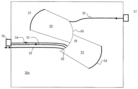
The basic operation of a subtractive double-grating architecture is
illustrated in Figure 4.
Input light of a given range of wavelengths is launched from an edge of a
planar lightwave
circuit (PLC) 20a via an input waveguide 21. The input light arrives at an
input 22 to a
first slab waveguide region 23, which includes a first concave reflective
diffraction grating
24. The first grating 24 focuses the light onto a focal line 26 at a position
that varies with
the wavelength. The focal line 26 (shown here as a Rowland circle, though
other
embodiments are possible) is also the focal line for a second concave
reflective diffraction
grating 27. The light from.the first grating 24, which was focused along the
focal line 26,
passes through a gap 28 into a second slab waveguide 29 and illuminates the
second
grating 27. Light outside the given range of wavelengths does not pass through
the gap
28, and could be collected by additional waveguides extending froru tl-~e
edge~of the chip
20a to the first waveguide region 23, as hereinafter described. The second
grating 27 re-
focuses the light onto an output point 31, where it is captured by an output
waveguide 32
and extracted. The location of the output point 31 and the parameters (order m
and pitch
A) of the second grating 27 are chosen to exactly compensate for the variation
along the
focal line 26 from the first grating 24 due to changes in wavelength.
Consequently the
light from the input waveguide 21 images onto the output point 31 and is
extracted to the
output of the device regardless of wavelength. The device is expected to have
a flat
transmission versus wavelength. In practice the transmission will not be
completely
wavelength independent for various reasons. The focal line 26 of the first
grating 24 can
only approximate the focal Iine of the second grating 27, except in the
special case of flat-
field design. Even still, the illumination of the second grating 27 will vary
as the input
position to the second grating 27 is varied along the focal line 26.
Nonetheless, substantial
flattening of the wavelength dependent transmission is achievable.
With reference to Figure 5, the subtractive double-grating device according to
the present
invention c an a lso be a sed as a Wavelength D ivision
Multiplexer/Demultiplexer, more
specifically as a band drop or band pass-through multiplexer, in which light,
with a
plurality of wavelength channels, is launched via a first port, i.e. the input
waveguide 21,
at the first concave reflective grating 24. The first grating 24 separates one
or more of the
wavelength channels, within a first wavelength range, and focuses them on
individual
output waveguides, e.g. 33 anal 34. The remaining light, i.e. in a second
wavelength range
with higher or lower wavelengths, passes through the gap 28 onto the second
reflective
grating 27, which directs and focuses the light, i.e. within the second
wavelength range,
6
CA 02560329 2006-09-19
WO 2005/091032 PCT/CA2005/000352
onto the waveguide 32, with a passband up to 2, 3, 4 or 5 times wider than the
channels
output the output waveguides 33 and 34. Light, within the wavelength range
which passes
through the gap 28, launched into the first slab waveguide region 23 from
another input
waveguide 41, will couple to a different output waveguide, e.g. waveguide 42.
The same architecture can be used for multiplexing optical wavelength channels
launched
via the waveguide 32 with optical wavelength channels launched via the
waveguides 33
and 34. The wavelength channels from the waveguide 32, within the second
wavelength
range, pass from the second grating 27, through the gap 28, off the fii~st
grating 24, onto
the waveguide 21. The wavelength channels from the waveguides 33 arid 34,
within the
first wavelength range, are directed off the first grating 24 onto the
waveguide 2 i .
With reference to Figure 6, to create a triplexer, the features of Figs. 4 and
5 are
combined. Input light carrying the two (or more) information channels (e.g.
1490 nm and
1550 nin) is launched via the waveguide 21, which becomes an input/output
waveguide
optically coupled to an FTTH optical network. The first concave reflective
grating device
24 disperses the input light into selected wavelengths in a manner convenient
with the 20
to 30 nm passbands, and focuses the dispersed sub-beams onto the ends of the
first and
second output w aveguides 33 and 34, r espectively, w hich lie a long a focal
1 ine 2 6. I f
necessary, additional output waveguides can be added adjacent the first and
second
waveguides 33 and 34 to capture other desired wavelengths. An array of photo-
detectors
36 (e.g. photo-diodes) are placed at the opposite ends of the output
waveguides 33 and 34
for converting the optical signals into electrical signals.
The outgoing signal light wavelength channel (or channels), e.g. at 1310 nm,
traveling in
the opposite direction, originates from a laser source 37 optically coupled to
an edge of
the PLC 20. The required physical dispersion is too high for the laser channel
to be
captured in one waveguide. Instead, the laser light is launched via the
waveguide 32
extending t o t he focal 1 ine 26 i nto t he s econd slab w aveguide region 2
9 a t the s econd
concave reflective grating 27, which focuses the light along the focal line
26, and which
directs t he light through the gap 2 8 t o the first concave reflective g
rating 2 4, w hick i s
shaped to collapse the dispersed radiation into the input/output waveguide 21.
The
physical w avelength d ispersion of the second grating 27 is o pposite t o
that o f t he first
grating 24 ( subtractive d ispersion), thereby reducing, a liminating, or
reversing the n et
7
CA 02560329 2006-09-19
WO 2005/091032 PCT/CA2005/000352
physical dispersion with respect to wavelength for light experiencing both
gratings. Since
the reflective gratings 24 and 27 are aligned, as above, to stabilize the
output angle for
different wavelengths, the path followed by the laser channel is reversible
for any
wavelength in the range of wavelengths, which would travel through the gap 28.
As demonstrated in Fig~ire 7, an extremely flat transmission passband over
100nm wide is
achieved for the ~ 1310 nm laser wavelength based on the use of t wo g ratings
in the
subtractive dispersion configuration. The detector channels at 1490 nm and
1550 nm
respectively encounter only one grating, and they are dispersed into narrow
bands.
In the VDV processor, isolation of close to ~0 dB is sometimes required
between the laser
source at 1310 nm and the receiver channels at 1490 and 1550 nm. In a grating-
based
device the main s ource o f background light arises from s cattering from d
efects o n the
facet profile. The facets themselves are arranged to create phase coherent
interference to
disperse and focus light in a wavelength specific manner. Corner rounding
between the
reflective facet and the non-reflective sidewall will also be periodic, and
therefore
spatially coherent, but with an inappropriate phase, leading to periodic ghost
images with
low intensity. Facet roughness will be spatially incoherent, leading to random
low-level
background light. Thus, if a strong laser signal is incident on a grating and
receiver
channels are also obtained from that grating, the receiver channels will have
a strong
background contributed from the laser, at a level typically 30 dB below the
strength of the
laser. Isolation of ~ 50 dB is closer to the requirement for a practical VDV
processor.
If a second grating is placed at the output of a first grating, and the order
(m~), pitch (Az)
and angles are chosen correctly, it is also possible to vary the output angle
of the second
grating with respect to wavelength by taking advantage of both the change in
wavelength
and the change in input angle to the second grating due to the dispersion of
the first
grating.
Figure 8 illustrates the basic operation of an additive double diffraction
grating
architecture designed to improve the isolation of the laser from the
receivers. An input
signal, comprising a plurality of optical wavelength channels, is launched
from an edge of
a P LC 5 Oa a long a n i nput w aveguide 51 t o a n i nput p ort 5 2 o f a
first s lab waveguide
region 53. The signal is directed to a first concave diffraction grating 54,
which disperses
8
CA 02560329 2006-09-19
WO 2005/091032 PCT/CA2005/000352
the input signal into constituent wavelength channels, and focuses. them along
a focal line
56 with position that varies with the wavelength. The focal line 56 (shown
here as a
Rowland circle, though other embodiments are possible) is also the focal line
for a second
concave diffraction grating 57. The light, which is within a specific
wavelength range,
travels through a gap 58, across a second waveguide region 59 to the second
grating 57.
The second grating 57 disperses the light even further, and re-focuses the
various
wavelength channels at output points 61a, 61b etc along the focal line 56,
where they are
captured by one of the output waveguides 62a, 62b etc, depending upon
wavelength. The
locations of the output points 61a, 61b etc, and the parameters (order m and
pitch A) of
the second grating 57, are chosen to enhance the variation along the focal
line 56 from the
second grating 57 dae to changes ire wavelength, creating an eve? greater
physical
dispersion at the output points 61a, 61b etc. Consequently the light from the
input
waveguide 51 images onto the output points 61 a, 61 b etc and is extracted to
the output of
the device with a dispersion that is greater than achievable with the first or
second grating
54 and 57, respectively, alone. The device is expected to have a narrower
transmission
band versus wavelength as compared with a device using only one of the
gratings.
With reference to Figure 9, minor modifications, e.g. an additional input
waveguide 63,
have been made to the additive double diffraction grating of Fig. 8 to provide
the
functionality of a Triplexer. Laser light at 1310 nm enters from the edge of
the chip SOb
from laser 64 into the input guide 63, which has an end positioned on the
focal line 56,
and propagates through the first slab waveguide region 53 onto the first
concave reflective
grating device 54. The grating 54 multiplexes the input light in a manner
convenient with
the 100 nm passband of the laser channel into the first waveguide 51, acting
as an
input/output waveguide, which also has an end along the focal line 56. The
light exits the
first inputloutput waveguide 51 in the direction to the chip a dge for
transmission to a
FTTH network. The incoming light at 1490 nm and 1550 nm enters the first
input/output
waveguide 51 traveling in the direction opposite to the laser light at 1310
nm. The light at
1490nm and 1550nm propagates through the frst slab waveguide 53 onto the first
concave reflective grating device 54, to be dispersed near the focal line 56.
The required
physical dispersion of the light is designed to b a too low to adequately
distinguish the
detector channels from this first grating device 54. The light propagates
through the gap
58 to the second slab waveguide region 59 onto the second concave reflective
grating 57,
which is structured to enhance the dispersion, so that the 1490 nm and 1550 nm
channels
9
CA 02560329 2006-09-19
WO 2005/091032 PCT/CA2005/000352
are dispersed sufficiently to be received by output waveguides 62a and 62b,
respectively,
the' ends of which also lie on the focal line 56. The two channels with 20nm
to 30nm
passbands exits towards the chip a dge to enter photo-detectors 66a and 66b.
The path
followed by the laser channel is reversible for that particular wavelength
band, i.e. 1260 to
1360 nm. Since the laser radiation at 1310 nm has been extracted immediately
upon
striking the first grating 54, the only radiation at 1310 nm striking the
second grating 57
will arise from scattering off the first grating 54. The intensity is expected
to be ~ 30 dB
below the laser intensity. The radiation at 1310 nm is further attenuated by ~
30 dB upon
striking the second grating 57, as viewed at waveguides 62a or 62b, because
those
waveguides are positioned to capture radiation at 1490 and 1550 nm. Thus ~ 60
dB
isolation of laser radiation from the detector channels should be possible.
Accordingly,
the Additive Dispersion architechire achieves an extremely high level of
isolation.
Similar to the subtractive double diffraction grating architecture a first
range of
wavelengths launched from the input/output waveguide 51 or the input waveguide
63 is
directed along the focal line 56, but stays in the first slab waveguide region
54, while a
second range of wavelengths passes through the gap 5~ to the second grating
57.
Contrary to the subtractive architecture, the range of wavelengths containing
the 1310 nm
channel launched via the input/output waveguide 51 stays in the first slab
waveguide
region 53, while the range of wavelengths including the detector channels 1490
nm and
1550 nm passes through the gap 5~ onto the second grating 57.
As demonstrated in Figure 10, narrow transmission passbands are achieved for
detector
channels whereas the laser channel is quite broad. The detector channels at
1490 nm and
1552 nm respectively encounter two gratings, and they are dispersed into
narrow bands,
i.e. 20nm to 30nm wide. The 1310 nm radiation is extracted following only one
grating,
i.e. with a passband of over 100nm, which improves the isolation of the laser
radiation
from detector channels to a level of over 45 dB in the case shown above. This
level of
isolation is significantly improved from the typical level of 30 dB from a
standard grating,
and is only made possible through the use of the dual-grating additive
dispersion
architecture.