Note: Descriptions are shown in the official language in which they were submitted.
CA 02560701 2006-09-21
WO 2005/099310
PCT/US2005/010051
ROLL-TO-ROLL FABRICATED LIGHT SHEET AND ENCAPSULATED
SEMICONDUCTOR CIRCUIT DEVICES
CROSS-REFERENCE TO RELATED APPLICATIONS
This is a PCT Application of US Patent Applications Serial Numbers 11/029,129
and 11/029,137, both entitled Roll-to-Roll Fabricated Light Sheet and
Encapsulated Semiconductor Circuit Eleinents, which are a Continuation-in-Part
of US Utility Application Serial Number 10/919,830, entitled Light Active
Sheet
And Methods For Making The Same, filed August 17, 2004, which is a US Utility
Application of US Provisional Application Serial Number 60/556,959, filed
March 29, 2004. This application is also a Continuation-in-Part of US Utility
Application Serial Number 10/920,010, entitled Light Active Sheet Material,
filed
August 17, 2004 and US Utility Application Serial Number 10/919,915 entitled
Photo-Radiation Source, filed August 17, 2004.
BACKGROUND OF THE INVENTION
The present invention pertains to a semiconductor roll-to-roll manufacturing
method. The present invention also pertains to an inorganic light emitting
diode
light sheet and methods for manufacturing the same. More particularly, the
present invention pertains to an inorganic light emitting diode light sheet
that can
be used as a photo-radiation source for applications including, but not
limited to,
' general illumination, architectural lighting,, novelty lighting, display
backlighting,
heads-up displays, commercial and roadway signage, monochromatic and full-
color static and video displays, a radiation-source for photo-curable
materials,
patterned light emissive images, and the like. Further, the present invention
pertains more particularly to an inorganic light active sheet that can be used
as a
light-to-energy device for converting photo-radiation to electrical energy for
applications including, but not limited to, solar panels, CCD-type cameras,
photo-
sensors, and the like. Further, the present invention pertains more
particularly, to
methods for mass-producing the inventive light active sheet at relatively low
cost.
CA 02560701 2006-09-21
WO 2005/099310
PCT/US2005/010051
Inorganic light emitting diodes (LED) are based on elements of the periodic
table
of a vast variety. They come out of semiconductor technology, and indeed, a
semiconductor diode such as a silicon diode, or a germanium diode were among
the first semiconductor devices. These were made by doping the silicon or the
germanium with a small amount of impurity to make n-type (excess electrons) or
p-type (excess holes) in the material. LEDs emit light because of the
materials
selected so that the light is emitted in the ultra-violet, visible, or
infrared ranges of
the spectrum. The types of materials used are made from vapor deposition of
materials on semiconductor wafers and cut into dice (a single one is a die).
Typically, the die, or LED dice, are about 12 mil sq. The composition of the
dice
depends on the color, for example some red dice are AlInGaAs and some blue
dice are InGaN. The variations are typically "three-five" variations, so-
called
because they vary based on the third and fifth period of the periodic table to
provide the n- and p-type materials.
The conversion of an LED die into an LED lamp is a costly process, involving
very precise handling and placement of the tiny LED die. The LED dice are most
simply prepared as 3 mm LED lamps. The die is robotically placed in a split
cup
with electrodes on each side. The entire structure is encased in a plastic
lens that
attempts to focus the beam more narrowly. High brightness dice may also be
surface mounted with current-driving and voltage limiting circuits, and
elaborate
heat sink and heat removal schemes. Connection is by soldering or solderless
ultrasonic wire bond methods. The result is a discrete point source of light.
The
LED lamp has a pair of leads, which can then be soldered to a printed circuit
board. The cost of forming the lamp and then soldering the lamp to a printed
circuit board is a relatively expensive process. Accordingly, there is a need
to
reduce the cost of forming alight emitting device based on the LED die.
As an example application of LED lamps, it has recently been shown that
ultraviolet LED lamps can be used to cure photo-polymerizable organic
materials
2
CA 02560701 2006-09-21
WO 2005/099310
PCT/US2005/010051
(see, for example, Loctite 7700 Hand Held LED Light Source, Henkel-Loctite
Corporation, Rocky Hill, CT).
Photo-polymerizable organic materials are well known and are used for
applications such as adhesives, binders and product manufacturing. Photo-
polymerization occurs in monomer and polymer materials by the cross-linking of
polymeric material. Typically, these materials are polymerized using radiation
emitted from sources of light including intensity flood systems, high
intensity
wands, chambers, conveyors and unshielded light sources.
As an example use of photo-polymerizable organic materials, precision optical
bonding and mounting of glass, plastics and fiber optics can be obtained with
photo-polymerizable adhesives. These materials can be used for opto-mechanical
assembly, fiber optic bonding and splicing, lens bonding and the attachment of
ceramic, glass, quartz, metal and plastic components.
Among the drawbacks of the conventional systems that utilize photo-
polymerizable organic materials is the requirement of a high intensity photo-
radiation source. Typically, light sources, such as mercury vapor lamps, have
been used to generate the radiation needed for photo-polymerization. However,
these light sources are an inefficient radiation source because most of the
energy
put in to drive the lamp is wasted as heat. This heat must be removed from the
system, increasing the overall bulk and cost. Also, the lamps have relatively
short
service life-times, typically around 1000 hours, and are very costly to
replace.
The light that is output from these light sources usually covers a much
broader
spectrum than the photo-radiation wavelengths that are needed for photo-
polymerization. Much of the light output is wasted. Also, although the
material
can be formulated to be hardened at other wavelengths, the typical photo-
polymerizable organic material is hardened at one of the peak output
wavelengths
of the mercury vapor lamp, to increase the polymerization efficiency. This
peak
3
CA 02560701 2006-09-21
WO 2005/099310
PCT/US2005/010051
output wavelength is in the UV region of the radiation spectrum. This UV'
radiation is harmful to humans, and additional shielding and protective
precautions such as UV-filtering goggles are needed to protect the operators
of
such equipment.
Figure 66 is a side view of an inorganic LED die available. A conventional
inorganic LED die is available from many manufacturers, typically has a
relatively narrow radiation emission spectrum, is relatively energy efficient,
has a
long service life and is solid-state and durable. The die shown is an example
of an
AlGaAs/AlGaAs red die, obtained from Tyntek Corporation, Taiwan. These dice
have dimensions roughly 12 mil x 12 mil x 8 mil, making them very small point
light sources. As shown in Figure 67, in a conventional LED lamp, this die is
held in a metal cup so that one electrode of the die (e.g., the anode) is in
contact
with the base of the cup. The metal cup is part of an anode lead. The other
electrode of the die (e.g,, the cathode) has a very thin wire soldered or wire
bonded to it, with the other end of the wire soldered or wire bonded to an
anode
lead. The cup, die, wire and portions of the anode and cathode leads are
encased
in a plastic lens with the anode and cathode leads protruding from the lens
base.
These leads are typically solder or wire bonded to a circuit board to
selectively
provide power to the die and cause it to emit light. It is very difficult to
manufacture these conventional lamps due to the very small size of the die,
and
the need to solder or wire bond such a small wire to such a small die
electrode.
Further, the plastic lens material is a poor heat conductor and the cup
provides
little heat sink capacity. As the die heats up its efficiency is reduced,
limiting the
service conditions, power efficiency and light output potential of the lamp.
The
bulkiness of the plastic lens material and the need to solder or wire bond the
lamp
leads to an electrical power source limits emissive source packing density and
the
potential output intensity per surface area.
4
CA 02560701 2006-09-21
WO 2005/099310
PCT/US2005/010051
There is a need for a photo-radiation source that is energy efficient,
generates less
heat, is low cost and that has a narrow spectrum of radiation emission. There
have been attempts to use inorganic light emitting diode lamps (LEDs) as photo-
radiation sources, Usually, these LEDs are so-called high brightness UV
radiation
sources. A typical LED consists of a sub-millimeter sized die of light
emitting
material that is electrically connected to an anode lead and a cathode lead.
The
die is encased within a plastic lens material. However, the processing that
takes
the LED dice and turns it into an LED lamp is tedious and sophisticated,
mostly
due to the very small size of the LED die. It is very difficult to solder or
wire
bond directly to the dice, and so it is common practice to use LED lamps that
are
then solder or wire bonded onto a circuit board. Conventionally, UV LED lamps
have been solder or wire bonded onto a circuit board in a formation to create
a
source of photo-radiation for photo-polymerizable organic materials.
This solution is far from optimum, since the relatively high cost of the LED
lamps
keeps the overall cost of the photo-radiation source high. There is a need for
a
photo-radiation source that can use the LED dice directly, without the need
for the
lamp construction or a direct solder or wire bonded connection between the
anode
and cathode of the die. Such as system would have an efficient die packing
density, enabling a high-intensity photo-radiation source having a narrow
emission band.
Wantanabe et al., published patent application US2004/0195576A1, teaches a
device and method for forming a transparent electrode over the light-emitting
portion of an LED die. This reference is concerned with overcoming the
difficulty of forming an electrode accurately at the light output surface of a
minute
LED device (10 square microns). A conventional LED is 300 square microns.
The reference states that forming a transparent electrode on a semiconductor
device so as not to shield emitted light is already known. The crux of the
Wantanabe invention is to form a transparent electrode directly and
specifically
CA 02560701 2006-09-21
WO 2005/099310
PCT/US2005/010051
over the light output face of a tiny LED device, or an array of such devices,
instead of the conventional bonding or soldering of an opaque wire to connect
the
LED device to a power supply line or lead. To form the transparent electrode
on
such a small device, this reference teaches the use of semiconductor and/or
printed circuit board techniques,
An example of the steps of forming the Wantanabe device consist of.
1) Providing a substrate
2) Forming p-side wiring on the substrate
3) Transferring a light emitting diode onto the substrate so the p side of the
diode
is connected to the wiring
4) Forming an insulation resin layer to cover the substrate, wiring and diode
5) Selectively removing the insulation resin to expose the n-side surfaces of
the
diode
6) Forming n-side wiring on the surface of the insulation resin
7) Forming a transparent electrode connecting the n-side of the diode to the n-
side
wiring
The steps for forming the transparent electrode are:
7a) Forming a resist film to cover the insulation resin and the exposed n-side
surfaces
7b) Selectively removing the resist layer to form an opening portion defining
the
light output surface of the diode and the n-side wiring
7c) Applying an electrode paste to the opening portion and the resist film
7d) Removing the electrode paste from the resist film to leave electrode paste
only
where the opening portion is so that the light output surface of the diode and
the
n-side wiring are connected.
There are variations disclosed to the various steps and materials used, but in
essence, the same cumbersome PCB-type processes are described in each of the
6
CA 02560701 2006-09-21
WO 2005/099310
PCT/US2005/010051
examples. This reference shows that it is known to form a transparent
electrode
using PCB techniques on the light output surface of a diode to reduce the
shielding of light emitted from the diode. But, replacing the conventionally-
used
opaque wire with a transparent electrode film is not new and is in the public
domain (see, Lawrence et al, US Patent 4,495,514).
Oberman, US Patent No. 5,925,897, teaches using a diode powder between
conductive contacts, forming a conductor/emissive layer/conductor device
structure. The diode powder consists of crystal particles 10-100 microns in
size.
The diode powder is formed by heating a mixture of In and Ga in a crucible and
flowing nitrogen gas over the heated mixture. This powder now contains all 11-
type material. The powder is adhered to a glass plate that is coated with an
appropriate contact metal. A p-type dopant is diffused into the powder
crystals to
form a p-region and the p-n diode junction. A top substrate with a transparent
conductive surface is placed on the powder and the entire structure thermally
annealed to enhance the adhesion of the powder to the upper contact, Oberman
states that the conventional LED is typically fabricated by connecting
electrical
contacts to the p and n regions of individual dies, and enclosing the entire
LED
die in a plastic package. Oberman's diode powder is specifically based on an
observation that surfaces, interfaces and dislocations appear to not adversely
affect the light emitting properties of nitrides. This reference says that
the
state-of-the-art nitride LED is grown on a sapphire substrate, and since
sapphire is
non-conducting, both electrical contacts are made from the top of the
structure.
Wickenden etal., US Patent No. 4,335,501, teaches a method for manufacturing a
monolithic LED array. The individual LEDs are formed by cutting isolation
channels through a slice of n-type material. The channels are cut in two
steps, a
first step is cutting a gap into the back of the slice of n-type material and
then this
gap is filled with glass. Then, in a second step the front of the slice is cut
to
complete the channel and the front cut is also filled with glass. Once the
isolation
7
CA 02560701 2006-09-21
WO 2005/099310
PCT/US2005/010051
channels have been formed, the tops of the remaining blocks of n-type material
are doped to become p-type and the n-p junction of each LED formed. Beam
leads are formed connecting the p-regions of the LEDs.
Nath, et al., W092/06144 and US 5, 273, 608, teaches a method for laminating
thin film photovoltaic devices with a protective sheet. The method provides
the
encapsulation of thin-film devices such as flexible solar cells within a top
insulating substrate and a bottom insulating substrate. Nath's description of
the
relevant prior art shows that encapsulating thin film devices between
insulating
sheets is not new. This reference teaches that the use of a heated roller is
undesirable. Nath's invention is to a specific method that heats a whole roll
of
composite material all at once to avoid the use of heated rollers. Nath
teaches a
new method for protecting and encapsulating thin film devices. Encapsulating
thin film devices between insulating sheets is not new, but Nath teaches a
specific
method that avoids the use of heated rollers.
SUMMARY OF THE INVENTION
The present invention is intended to overcome the drawbacks of the prior art.
It is
an object of the present invention to provide methods for manufacturing solid-
state light active devices. It is another object of the present invention to
provide
device structures for solid-state light active devices. It is still another
object of the
present invention to provide a photo-radiation source for the selective
polymerization of photo-radiation-curable organic material. It is yet another
object of the present invention to provide a method of making a light sheet
material. It is yet another object of the present invention to provide a
method of
manufacturing an encapsulated semiconductor circuit using a roll-to-roll
fabrication process.
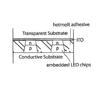
The present invention pertains to a method of making a light active sheet. A
bottom substrate having an electrically conductive surface is provided. A
hotmelt
8
CA 02560701 2006-09-21
WO 2005/099310
PCT/US2005/010051
adhesive sheet is provided. Light active semiconductor elements, such as LED
die, are embedded in the hotmelt adhesive sheet. The LED die each has a top
electrode and a bottom electrode. A top transparent substrate is provided
having a
transparent conductive layer. The hotmelt adhesive sheet with the embedded LED
die is inserted between the electrically conductive surface and the
transparent
conductive layer to form a lamination. The lamination is run through a heated
pressure roller system to melt the hotmelt adhesive sheet and electrically
insulate
and bind the top substrate to the bottom substrate. As the hotmelt sheet is
softened, the LEI) die breakthrough so that the top electrode comes into
electrical
contact with the transparent conductive layer of the top substrate and the
bottom
electrode comes into electrical contact with the electrically conductive
surface of
the bottom substrate. Thus, the p and n sides of each LED die are
automatically
connected to the top conductive layer and the bottom conductive surface. Each
LED die is encapsulated and secured between the substrates in the flexible,
hotmelt adhesive sheet layer. The bottom substrate, the hotmelt adhesive (with
the
embedded LED die) and the top substrate can be provided as rolls of material.
The rolls are brought together in a continuous roll fabrication process,
resulting in
a flexible sheet of lighting material.
This simple device architecture is readily adaptable to a high yield, low
cost, roll-
to-roll fabrication process. Applicants have proven the device architecture
and
method are effective by making many proof-of-concept prototypes. Figure 119
shows photographs of working prototypes constructed in accordance with the
inventive method for manufacturing an inorganic light sheet. Figure 128(a) is
a
photograph showing a step of the proof-of-concept prototype construction, this
photo shows an active layer sheet comprised of LED die embedded in a sheet of
hotmelt adhesive, the LED die being red emitting and yellow emitting. Figure
128(b) is a photograph showing another step of the proof-of-concept prototype
construction, this photo shows the three constituent layers - active layer
sheet
(LED die embedded in a sheet of hotmelt adhesive), a top substrate (ITO coated
9
CA 02560701 2006-09-21
WO 2005/099310
PCT/US2005/010051
PET) arid a bottom substrate (ITO coated PET). Figure 128(c) is a photograph
showing another step of the proof-of-concept prototype construction, this
photo
shows the three constituent layers with the active layer between the
substrates to
form an assembly. Figure 128(d) is a photograph showing another step of the
proof-of-concept prototype construction, this photo shows the assembled
lamination being passed through a heat laminator to activate the hotmelt sheet
by
melting between pressure rollers.
Applicants have discovered that as the hotmelt sheet is softened, the LED dice
breakthrough the adhesive so that the top electrode comes into electrical
contact
with the transparent conductive layer of the top substrate and the bottom
electrode
comes into electrical contact with the electrically conductive surface of the
bottom
substrate. Thus, the p and n sides of each LED die are automatically connected
to
the top conductive layer and the bottom conductive surface. Each LED die is
completely encapsulated within the hotmelt adhesive and the substrates. In
addition, the LED dice are each permanently secured between the substrates in
the
flexible, hotmelt adhesive sheet layer. Figure 128(e) is a photograph showing
the
just constructed proof-of-concept prototype being applied a voltage of a
polarity
and lighting up the yellow LED die. Figure 128(t) is a photograph showing the
just constructed proof-of-concept prototype being applied a voltage of the
opposite polarity and lighting up the red LED die.
In accordance with an aspect of the present invention, a method of making a
light
active sheet is provided. A bottom substrate having an electrically conductive
surface is provided. An electrically insulative adhesive is provided. Light
active
semiconductor elements, such as LED die, are fixed to the electrically
insulative
adhesive. The light active semiconductor elements each have an n-side and a p-
side. A top transparent substrate is provided having a transparent conductive
layer.
CA 02560701 2006-09-21
WO 2005/099310
PCT/US2005/010051
The electrically insulative adhesive having the light active semiconductor
elements fixed thereon is inserted between the electrically conductive surface
and
the transparent conductive layer to form a lamination. The electrically
insulative
adhesive is activated to electrically insulate and bind the top substrate to
the
bottom substrate. The device structure is thus formed so that either the n-
side or
the p-side of the light active semiconductor elements are in electrical
communication with the transparent conductive layer of the top substrate, and
so
that the other of the n-side or the p-side of each the light active
semiconductor
elements are in electrical communication with the electrically conductive
surface
of the bottom substrate to form a light active device. In accordance with the
present invention, p and n sides of each LED die are automatically connected
and
maintained to the respective top and bottom conductor, completely securing
each
LED die between the substrates in a flexible, hotmelt adhesive sheet layer.
The bottom substrate, the electrically insulative adhesive and the top
substrate can
be provided as respective rolls of material. This enables the bottom
substrate, the
electrically ins -ulative adhesive (with the LED die embedded therein) and the
top
substrate together in a continuous roll fabrication process. It is noted that
these
three rolls are all that are necessary for forming the most basic working
device
structure in accordance with the present invention. This simple and
uncomplicated structure is inherently adaptable to a high yield, continuous,
roll-
to-roll fabrication techniques that is not obtainable using prior art
techniques.
In a preferred embodiment, the electrically insulative adhesive comprises a
hotmelt material. The step of activating comprises applying heat and pressure
to
the lamination to soften the hotmelt material. At least one of the heat and
pressure
are provided by rollers. Alternatively, the adhesive may be composed so that
activating it co mprises at least one of solvent action (e.g., silicone
adhesive),
catalytic reaction (e.g., epoxy and hardner) and radiation curing (e.g., UV
curable
polymer adhesive).
11
CA 02560701 2006-09-21
WO 2005/099310
PCT/US2005/010051
The light active semiconductor elements can be light emitting diode die such
as is
readily commercially available from semiconductor foundries. The light active
semiconductor elements may alternatively or additionally be light-to-energy
devices, such as solar cell devices. To make white light, a first portion of
the light
active semiconductor elements emit a first wavelength of radiation and second
portion of the light active semiconductor elements emit a second wavelength of
radiation. Alternatively, yellow light emitting LED die and blue light
emitting
LED die can be provided in proper proportions to create a desired white light
appearance. Diffusers can be included within the adhesive, substrates or as a
coating on the substrates and/or the adhesive to create a more uniform glowing
surface.
The electrically insulative adhesive can be a hotmelt sheet material, such as
that
available from Bemis Associates, Shirley, MA. The light active semiconductor
elements can be pre-embedded into the hotmelt sheet before the step of
inserting
the adhesive sheet between the substrates. In this way, the hotmelt sheet can
have
the semiconductor devices embedded off-line so that multiple embedding lines
can supply a roll-to-roll fabrication line. A predetermined pattern of the
light
active semiconductor elements can be formed embedded in the hotmelt sheet.
The predetermined pattern can be formed by electrostatically attracting a
plurality
of light active semiconductor elements on a transfer member, similar to a
laser
printer electrostatic drum, and transferring the predetermined pattern onto
the
insulative adhesive.
The predetermined pattern of the light active semiconductor elements can be
formed by magnetically attracting a plurality of light active semiconductor
elements on a transfer member, such as an optomagnetically coated drum, and
transferring the predetermined pattern onto the insulative adhesive. The
predetermined pattern of the light active semiconductor elements can be formed
12
CA 02560701 2006-09-21
WO 2005/099310
PCT/US2005/010051
using conventional pick and place machines. Or, an adhesive transfer method,
described in detail herein, can be employed_ In this case, the predetermined
pattern is formed by transferring the semia>nductor elements from a relatively
lower tack adhesive to a relatively higher tack adhesive.
The transparent conductive layer can be forsned by printing a transparent
conductive material, such as ITO particles in a polymer binder, to form
conductive light transmissive connecting lands. Each land is provided for
connecting with a respective light active semiconductor. A relatively higher
conducting line pattern can be formed on at least one of the top substrate and
the
bottom substrate for providing a relatively lcwer path of resistance from a
power
supply source to each light active semiconductor element.
The electrically conductive surface and the electrically conductive pattern
may
comprise a respective x and y wiring grid fox selectively addressing
individual
light active semiconductor elements for forming a display.
Color light can be provided by including LED capable of emitting different
wavelengths of light. For example, a red emitting LED combined with a yellow
emitting LED when driven together and located near each other will be
perceived
by the human eye as generating an orange light. White light can be generated
by
combining yellow and blue LED dice, or red, green and blue dice. A phosphor
can be provided in the lamination. The phosphor is optically stimulated by a
radiation emission of a first wavelength (e.g., blue) from the light active
semiconductor element (e.g., LED die) to emit light of a second wavelength
(e.g.,
yellow).
In accordance with another aspect of the present invention, a method is
provided
for making an electronically active sheet. The electronically active sheet has
a
very thin and highly flexible form factor. It can be manufactured using the
low
13
CA 02560701 2006-09-21
WO 2005/099310
PCT/US2005/010051
cost, high yield continuous roll-to-roll fabrication method described herein.
The
electronically active sheet can be used for making a lighting device, a
display, a
light-to-energy device, a flexible electronic circuit, and many other
electronic
devices. The semiconductor elements can include resistors, transistors,
diodes,
and any other semiconductor element having a top and bottom electrode format.
Other electronic elements can be provided in combination or separately and
employed as components of the fabricated flexible electronic circuit. The
inventive steps for forming the electronically active sheet include providing
a
bottom planar substrate having an electrically conductive surface.
An adhesive is provided and at least one semiconductor element is fixed to the
adhesive. Each semiconductor element has a top conductor and a bottom
conductor, A top substrate is provided having an electrically conductive
pattern
disposed thereon.
The adhesive with semiconductor element fixed thereto is inserted between the
electrically conductive surface and the electrically conductive pattern to
form a
lamination. The adhesive is activated to bind the top substrate to the bottom
substrate so that one of top conductor and bottom conductor of semiconductor
element is automatically brought into and maintained in electrical
communication
with the electrically conductive pattern of the top substrate and so that the
other of
the top conductor and the bottom conductor of each semiconductor element is
automatically brought into and maintained in electrical communication with the
electrically conductive surface of the bottom substrate to form an
electronically
active sheet.
In accordance with another aspect of the present invention, a method is
provided
for making an encapsulated semiconductor device. A bottom substrate is
provided having an electrically conductive surface. An adhesive layer is
provided
on the electrically conductive surface. A predetermined pattern of
semiconductor
elements are fixed to the adhesive. The semiconductor elements each having a
top device conductor and a bottom device conductor. A top substrate having a
CA 02560701 2006-09-21
WO 2005/099310
PCT/US2005/010051
conductive pattern disposed thereon. A lamination is formed comprising the
bottom substrate, the adhesive layer (with the semiconductor elements) and the
top substrate. The lamination is formed so that the adhesive electrically
insulates
and binds the top substrate to the bottom substrate. In so doing, one of the
top
device conductor and bottom device conductor of the semiconductor elements is
in electrical communication with the conductive pattern of the top substrate
and
the other of the top device conductor and bottom device conductor of each
semiconductor element is in electrical communication with the elecArically
conductive layer of the bottom substrate. In this manner, each semiconductor
element is automatically connected to the top and bottom conductors that are
preformed on the top and bottom substrates. There is no need for wirebonding,
solder, lead wires, or other electrical connection elements or steps.
In accordance with another aspect of the present invention, at least one the
semiconductor elements is provided with a middle conductor region between the
top conductor and the bottom conductor. For example, the semiconductor can be
an npn or pnp transistor. The adhesive comprises at least one electrically
conductive portion for making an electrical connection with the middle
conductor
region.
The inventive light active sheet consists of a bottom substrate flexible sheet
having an electrically conductive surface. A top transparent substrate
flexible
sheet has a transparent conductive layer disposed on it. An electrically
insulative
adhesive flexible sheet has light active semiconductor elements fixed to it.
The
light active semiconductor elements each have an n-side and a p-side. The
electrically insulative adhesive sheet having the light active semiconductor
elements fixed to it is inserted between the electrically conductive surface
and the
transparent conductive layer to form a lamination, The adhesive sheet is
activated
so that the electrically insulative adhesive electrically insulates and binds
the top
substrate sheet to the bottom substrate sheet. When the adhesive sheet is
CA 02560701 2006-09-21
WO 2005/099310
PCT/US2005/010051
activated, one of the n-side or the p-side of the light active semiconductor
elements is automatically brought into electrical communication with the
transparent conductive layer of the top substrate sheet_ The other of the n-
side or
the p-side is automatically brought into electrical comtnunication with the
electrically conductive surface of the bottom substrate sheet to form a light
active
device.
Due to the automatic assembly nature of the inventive light sheet, the bottom
substrate, the electrically insulative adhesive and the tc,p substrate can be
provided
as respective rolls of material. The electrically insulative adhesive can have
the
semiconductor elements pre-embedded into it and re-rolled, or the embedding of
the semiconductor elements can be performed in line during the fabrication
process. The adhesive is inserted between the substrates by bringing the
bottom
substrate, the electrically insulative adhesive and the top substrate together
in a
continuous roll fabrication process.
The electrically insulative adhesive preferably comprises a hotmelt material
activatable by applying heat and pressure to the lamination to soften the
hotmelt
material. Alternatively, or additionally, the adhesive may be activatable by
at
least one of solvent action, evaporation, catalytic reaction and radiation
curing.
The light active semiconductor elements can be light emitting diode die, or
other
semiconductor and circuit elements, such as transistors, resistors,
conductors, etc.
They can be connected in an electronic circuit through the inventive hotmelt
lamination method described herein. Further, the light active semiconductor
elements can be light-to-energy devices, such as diodes effective for
converting
sunlight to electrical energy.
In the case of light emitting diodes, a first portion of the light active
semiconductor elements can emit a first wavelength of radiation and a second
16
CA 02560701 2006-09-21
WO 2005/099310
PCT/US2005/010051
portion of the light active semiconductor elements emit a second wavellgth of
radiation. With this construction, the light active sheet can be effective fbr
generating multiple colors and white light.
The electrically insulative adhesive can comprise a hotmelt sheet material,
and the
light active semiconductor elements can be pre-embedded into the hotmelt sheet
before forming the lamination. The light active semiconductor elements can be
formed into a predetermined pattern. The predetermined pattern can be formed
by
electrostatically attracting a plurality of light active semiconductor
elernamts on a
transfer member and transferring the predetermined pattern onto the
insitlative
adhesive. Alternatively, or additionally, the light active semiconductor
elements
can be formed into the predetermined pattern by magnetically attracting the
plurality of light active semiconductor elements on a transfer member and
transferring the predetermined pattern onto the insulative adhesive.
The transparent conductive layer may comprise a transparent conductive
material
formed as conductive light transmissive connecting lands, each land for
connecting with a respective light active semiconductor. A relatively higher
conducting line pattern can be formed on at least one of the top substrate and
the
bottom substrate for providing a relatively lower path of resistance from
power
supply source to each light active semiconductor element.
The electrically conductive surface and the electrically conductive pattern_
can
comprise a respective x and y wiring grid for selectively addressing
individual
light active semiconductor elements for forming a display.
A phosphor can be provided in the lamination. The phosphor is optically
stimulated by a radiation emission of a first wavelength from the light active
semiconductor element to emit light of a second wavelength. With this
17
CA 02560701 2006-09-21
WO 2005/099310
PCT/US2005/010051
construction, white light can be generated using a blue emitting LED and
yellow
emitting phosphors.
In accordance with another aspect of the present invention, an electronically
active sheet comprises a bottom planar substrate having an electrically
conductive
surface. A top substrate having an electrically conductive pattern disposed
thereon is also included. At least one semiconductor element having a top
conductor and a bottom conductor is embedded in an adhesive sheet. The
adhesive sheet is disposed between the electrically conductive surface and the
electrically conductive pattern to form a lamination. The adhesive is
activatable
to bind the top substrate to the bottom substrate so that either the top
conductor or
the bottom conductor of the semiconductor element is automatically brought
into
and maintained in electrical communication with the electrically conductive
pattern of the top substrate. The other of the top conductor and the bottom
conductor of each semiconductor element is also automatically brought into and
maintained in electrical communication with the electrically conductive
surface of
the bottom substrate to form an electronically active sheet.
With this construction, an electronically active sheet is formable using a
high
yield roll-to-roll fabrication method. In this case, the bottom substrate, the
adhesive and the top substrate are all provided as respective rolls of
material. The
bottom substrate, the adhesive and the top substrate are brought together in a
continuous roll fabrication process. The adhesive may comprise a hotmelt sheet
material activatable by applying heat and pressure to the lamination to soften
the
hotmelt material. Alternatively, the adhesive is activatable by at least one
of
solvent action, evaporation, catalytic reaction and radiation curing of the
adhesive.
In any case, the adhesive can be provided as a sheet, and have the
semiconductor
elements pre-embedded into the sheet in a predetermined pattern before forming
the lamination. Or, the adhesive can be printed, coated, or otherwise applied
onto
one of the substrates, and then the semiconductor elements disposed thereon.
18
CA 02560701 2006-09-21
WO 2005/099310
PCT/US2005/010051
The predetermined pattern of the semiconductor elements can be formed by
electrostatically attracting a plurality of the semiconductor elements on a
transfer
member and transferring the predetermined pattern onto the adhesive. The
predetermined pattern of the semiconductor elements can be formed by
magnetically attracting a plurality of the semiconductor elements on a
transfer
member and transferring the predetermined pattern onto the adhesive. The
predetermined pattern of the semiconductor elements can be formed using a pick
and place device.
In accordance with another aspect of the invention, an encapsulated
semiconductor device includes a bottom substrate having an electrically
conductive surface. A top substrate has an electrically conductive pattern
disposed thereon, the conductive pattern can be formed by coating, sputtering,
printing, photolithography or other pattern forming method. A predetermined
pattern of semiconductor elements, each semiconductor element having atop
device conductor and a bottom device conductor is fixed to an adhesive. The
adhesive is disposed between the electrically conductive surface and the
electrically conductive pattern to form a lamination. The adhesive is
activated to
bind the top substrate to the bottom substrate so that either the top
conductor or
the bottom conductor of each semiconductor element is automatically brought
into
and maintained in electrical communication with the electrically conductive
pattern of the top substrate. Also, the other of the top conductor or the
bottom
conductor of each semiconductor element is automatically brought into and
maintained in electrical communication with the electrically conductive
surface of
the bottom substrate to form an electronically active sheet.
In accordance with the present invention, the semiconductor elements includes
a
middle conductor region between the top conductor and the bottom conductor,
for
example, an n-p-n transistor element. The adhesive can comprise at least one
19
CA 02560701 2006-09-21
WO 2005/099310
PCT/US2005/010051
electrically conductive portion for making an electrical connection with the
middle conductor region.
The bottom substrate, the adhesive and the top substrate can be provided as
respective rolls of material and the lamination formed by bringing the bottom
substrate, the electrically insulative adhesive and the top substrate together
in a
continuous roll fabrication process.
The adhesive can be a hotmelt sheet material activatable by applying heat and
pressure to the lamination to soften the hotmelt material. The pattern of
semiconductor elements can be pre-embedded into the hotmelt sheet before
forming the lamination. The predetermined pattern of the semiconductor
elements can formed by electrostatically attracting a plurality of
semiconductor
elements on a transfer member and transferring the predetermined pattern onto
the
adhesive. The predetermined pattern of the semiconductor elements can be
formed by magnetically attracting the plurality of semiconductor elements on a
transfer member and transferring the predetermined pattern onto the adhesive.
The predetermined pattern of the semiconductor elements can be formed using a
pick and place device. The predetermined pattern of the semiconductor elements
can also be formed by transferring the semiconductor elements from a
relatively
lower tack adhesive to a relatively higher tack adhesive.
In accordance with the present invention, substrate sheets are provided with a
precoated transparent conductor film. The p and n sides of each LED die are
automatically connected to the respective top and bottom conductor, completely
securing each LED die between the substrates in a flexible, hotmelt adhesive
sheet
layer. There are no resist films to form, pattern and etch away. The
transparent
electrode is not necessarily formed only on each emissive device using
elaborate
semiconductor patterning and etching techniques.
CA 02560701 2006-09-21
WO 2005/099310
PCT/US2005/010051
In accordance with the present invention, LED die cut from a semiconductor
wafer are utilized as light sources. The die are typically 300 microns square
by
200 microns high. The inventive device includes conventional LED die between
sheets of conductive substrates.
In accordance with the present invention, a conductor/emissive layer/conductor
device structure has an emissive layer made from an array of commercially
available conventional LED die. A thin sheet of light is formed using a
continuous roll-to-roll manufacturing method, and using conventional LED die
that are commercially available from many sources.
In accordance with the inventive system, an unexpected result is obtained
wherein
an LED die array can be pre-embedded into a hotmelt sheet adhesive layer,
forming the active layer of the device. This active layer is disposed between
top
and bottom sheet substrates. When the hotmelt is heated, the entire structure
fuses
together, locking in the LED die between the substrates. There is solid and
flexible adhesive completely surrounding and securing each die, except at the
contact surfaces with the planar electrode, and permanently securing the top
substrate to the bottom substrate.
Apparently the hotmelt material does not wet the surface of the LED die and so
when the hotmelt material is melted, the p surface and the n surface of the
die
become exposed and make electrical contact with the conductive surfaces of the
top and bottom substrates. When the hotmelt adhesive cools and hardens, the
intimate electrical contact between the LED die and the conductive surfaces is
secured, making an extremely thin, easily formed, extremely robust and highly
flexible light sheet device.
The resulting device structure is easily manufactured in a continuous roll-to-
roll
process, there are no resist layers to form, pattern and remove, there is no
doping
21
CA 02560701 2006-09-21
WO 2005/099310
PCT/US2005/010051
in-place of the emissive elements, there are no alignment issues for making
contact with the p and n surfaces of the die. In the inventive system, these p
and n
surfaces automatically make contact with the respective conductive surfaces
when
the hotmelt is in its plastic or softened state and the lamination is placed
between
pressure rollers. Then, when the hotmelt hardens, the entire structure is
fused into
one coherent laminated composite sheet, with each die securely locked in
electrical contact with the planar conductors of the top and bottom
substrates. The
entire device consists of just three sheet layers (the two substrates and the
hotmelt/dice active layer) that can each be prepared off-line and put into
rolls.
The present invention is provided for making sheets of inorganic LED lighting
material. Substrate sheets may be utilized with precoated conductive films, or
the
conductive films can be printed and patterned directly onto the substrates.
One
film is a transparent conductor. The conductive films provide each of a
plurality
of LED die with a direct, face-to-face electrical connection, device-
protecting
resistance, and an optically transparent window for emitting light. In
accordance
with the present invention, when a hotmelt sheet melts under the pressure of a
heated pressure roller, the LED die are squeezed between the substrate sheets
and
the top and/or bottom face of each die breaks through the hotmelt adhesive
sheet
and comes in face-to-face contact with the precoated conductive films. This
enables each die to be automatically connected to the top and bottom
conductor.
In accordance with another aspect of the invention, a method is provided for
forming a sheet of light active material. A first substrate is provided having
a
transparent first conductive layer. A pattern of light active semiconductor
elements are formed. The light active semiconductor elements have an n-side
and
a p-side. Each light active semiconductor element has either of the n-side or
the
p-side in electrical communication with the transparent conductive layer. A
second substrate having a second conductive layer is provided. The second
substrate is secured to the first substrate so that the other of the n-side or
the p-
22
CA 02560701 2006-09-21
WO 2005/099310
PCT/US2005/010051
side of each light active semiconductor element in electrical communication
with
the second conductive layer. Thus, a solid-state sheet of light active
material is
formed.
The transparent first conductive layer may comprise a transparent coating
preformed on the first substrate. The transparent coating can be applied as a
conductive ink or conductive adhesive.
The pattern of light active semiconductor elements can be formed by
electrostatically attracting the light active semiconductor elements to a
transfer
member. Then, transferring the attracted light active semiconductor elements
from
the transfer member to the first substrate. The transfer member may include an
opto-electric coating effective for holding a patterned electrostatic charge.
The
patterned electrostatic charge is effective for electrostatically attracting
the light
active semiconductor elements and forming the pattern of light active
semiconductor elements. The optical patterning of the opto-electric coating
can be
done, for example, using a scanned laser beam and an LED light source, similar
to
the process used by laser or LED printers. Thus, the transfer member may
comprise a drum.
An adhesive pattern can be formed on the first substrate for adhering the
pattern
of light active semiconductor elements to the first substrate. Alternatively,
or
additionally, an adhesive pattern can also be formed on the first substrate
for
adhering the second substrate to the first substrate.
A pattern of light active semiconductor elements can be formed by forming a
first
pattern of first light active semiconductor elements and forming a second
pattern
of second light active semiconductor elements. The first light active
semiconductor elements emit light having a first color and the second light
active
semiconductor elements emit light having a second color. Alternatively, the
first
23
CA 02560701 2006-09-21
WO 2005/099310
PCT/US2005/010051
light active semiconductor elements emit light and the second light active
semiconductor elements convert light to electrical energy.
The first conductive layer may be formed as a grid of x-electrodes, and the
second
conductive layer formed as a grid of y-electrodes, so that each respective
light
active semiconductor element is addressable for forming a sheet of light
active
material capable of functioning as a pixelated display component.
The pattern of light active semiconductor elements can be formed by forming a
first pattern of first color light emitting semiconductor elements, forming a
second
pattern of second color light emitting semiconductor elements and forming a
third
pattern of third color light emitting semiconductor element. The first
conductive
layer may be formed as a grid of x-electrodes, and the second conductive layer
formed as a grid of y-electrodes, so that each respective light active
semiconductor is addressable for forming a sheet of light active material
capable
of functioning as a full-color pixelated display component.
In accordance with another aspect of the invention, a method is provided for
forming a light-emitting device. A first substrate is provided. A first
conductive
surface is formed on the first substrate. A pattern of LED dice is formed on
the
conductive pattern. Each LED die has an anode and a cathode side. A second
substrate is provided. A second conductive surface is formed on the second
substrate. The first substrate is fixed to the second substrate so that either
of the
anode and the cathode side of the LED die is in electrical communication with
the
first conductive surface, and the other of the anode and the cathode side of
the
LED dice is in electrical communication with the second conductive surface.
The first conductive surface may be formed as a conductive pattern comprised
of
at least one of a conductive coating, a conductive ink and a conductive
adhesive.
At least one of the first and the second conductive surface is a transparent
24
CA 02560701 2006-09-21
WO 2005/099310
PCT/US2005/010051
conductor. At least one of the first and the second conductive surface is
preformed on the respective first and second substrate. The first conductive
surface can be formed using a printing method. The printing method may
comprise at least one of an inkjet printing method, a laser printing method, a
silk-
screen printing method, a gravure printing method and a donor transfer sheet
printing method.
An adhesive layer may be formed between the top substrate and the bottom
substrate. The adhesive layer may comprise at least one of a conductive
adhesive,
a semi-conductive adhesive, an insulative adhesive, a conductive polymer, a
semi-
conductive polymer, and an insulative polymer. A function-enhancing layer can
be formed between the top substrate layer and the bottom substrate layer. The
function-enhancing layer includes at least one of a re-emitter, a light-
scatterer, an
adhesive, and a conductor.
The pattern of LED dice can be formed by electrostatically attracting the LED
dice to a transfer member, and then transferring the attracted LED dice from
the
transfer member to the first conductive surface. The transfer member may
include
an opto-electric coating effective for holding a patterned electrostatic
charge, the
patterned electrostatic charge being effective for electrostatically
attracting and
forming the pattern of LED dice.
The the opto-electric coating can be patterned using at least one of a scanned
laser
beam and an LED light source. The transfer member may be a drum, a flat planar
member, or other shape.
hi accordance with another aspect of the invention, a method is provided for
forming a light-to-energy device. A first substrate is provided. A first
conductive
surface is formed on the first substrate. A pattern of semiconductor elements
is
formed on the conductive pattern. Each semiconductor element comprises a
charge donor side and a charge acceptor side. A second substrate is provided.
A
CA 02560701 2006-09-21
WO 2005/099310
PCT/US2005/010051
second conductive surface is formed_ on the second substrate. The first
substrate is
fixed to the second substrate so that either of the charge donor and the
charge
acceptor side of the semiconductor elements is in electrical communication
with
the first conductive surface and the other of the charge donor and the charge
acceptor side of the semiconductor elements is in electrical communication
with
the second conductive surface.
The first conductive surface is formed as a conductive pattern comprised of at
least one of a conductive coating, a conductive ink and a conductive adhesive.
At
least one of the first and the second conductive surface is a transparent
conductor.
At least one of the first and the second conductive surface is prefonned on
the
respective first and second substrate_ The first conductive surface may be
formed
using a printing method. The printing method may comprise at least one of an
inkjet printing method, a laser printing method, a silk-screen printing
method, a
gravure printing method and a donor transfer sheet printing method.
An adhesive layer can be formed between the top substrate and the bottom
substrate. The adhesive layer may comprise at least one of a conductive
adhesive,
a semi-conductive adhesive, an insulative adhesive, a conductive polymer, a
semi-
conductive polymer, and an insulative polymer. A function-enhancing layer can
be formed between the top substrate layer and the bottom substrate layer,
wherein
the function-enhancing layer includes at least one of a re-emitter, a light-
scatterer,
an adhesive, and a conductor.
The pattern of LED dice can be formed by electrostatically attracting the LED
dice to a transfer member, and then transferring the attracted LED dice from
the
transfer member to the first conductive surface. The transfer member may
include
an opto-electric coating effective for holding a patterned electrostatic
charge, the
patterned electrostatic charge being effective for electrostatically
attracting and
forming the pattern of LED dice. The opto-electric coating can be patterned
using
26
CA 02560701 2006-09-21
WO 2005/099310
PCT/US2005/010051
at least one of a scanned laser beam and an LED light source. The transfer
member may be shaped as a drum, a flat planar member, or other shape.
In accordance with another aspect of the invention, device structures are
provided
for sheets of light active material. A first substrate has a transparent first
conductive layer. A pattern of light active semiconductor elements fixed to
the
first substrate. The light active semiconductor elements have an n-side and a
p-
side. Each light active semiconductor element has either of the n-side or the
p-
side in electrical communication with the transparent conductive layer. A
second
substrate has a second conductive layer. An adhesive secures the second
substrate
to the first substrate so that the other of the n-side or the p-side of each
light
active semiconductor element is in electrical communication with the second
conductive layer. Thus, a solid-state light active device is formed.
The transparent first conductive layer may comprise a transparent coating
preformed on the first substrate. The transparent coating can be a conductive
ink
or conductive adhesive. An adhesive pattern may be formed on the first
substrate
for adhering the pattern of light active semiconductor elements to the first
substrate. Alternatively, or additionally, an adhesive pattern may be formed
on
the first substrate for adhering the second substrate to the first substrate.
The pattern of light active semiconductor elements may comprise a first
pattern of
first light active semiconductor elements and a second pattern of second light
active semiconductor elements. The first light active semiconductor elements
may emit light having a first color and the second light active semiconductor
elements emit light having a second color. Alternatively, the first light
active
semiconductor elements may emit light and the second light active
semiconductor
elements convert light to electrical energy.
27
CA 02560701 2006-09-21
WO 2005/099310
PCT/US2005/010051
The first conductive layer may be formed as a grid of x-electrodes, and the
second
conductive layer formed as a grid of y-electrodes. Each respective light
active
semiconductor element is disposed at the respective intersections of the x and
y
grid and are thus addressable for forming a sheet of light active material
capable
of functioning as a pixelated display component.
The pattern of light active semiconductor elements may comprise a first
pattern of
first color light emitting semiconductor elements, a second pattern of second
color
light emitting semiconductor elements and a third pattern of third color light
emitting semiconductor element. The first conductive layer may be formed as a
grid of x-electrodes, and the second conductive layer being formed as a grid
of y-
electrodes. The respective first, second and third color light emitting
elements
may be disposed at the intersections of the x and y grid so that each
respective
light active semiconductor is addressable. Thus, a sheet of light active
material is
formed capable of functioning as a full-color pixelated display component.
In accordance with another aspect of the invention, a light-emitting device
comprises a first substrate. A first conductive surface is formed on the first
substrate. A pattern of LED dice is formed on the conductive pattern. Each LED
die has an anode and a cathode side. A second substrate has a second
conductive
surface formed on it. An adhesive fixes the first substrate to the second
substrate
so that either of the anode and the cathode side of the LED die is in
electrical
communication with the first conductive surface, and the other of the anode
and
the cathode side of the LED dice is in electrical communication with the
second
conductive surface.
The first conductive surface can be formed as a conductive pattern comprised
of
at least one of a conductive coating, a conductive ink and a conductive
adhesive.
At least one of the first and the second conductive surface is a transparent
conductor. At least one of the first and the second conductive surface can be
28
CA 02560701 2006-09-21
WO 2005/099310
PCT/US2005/010051
preformed on the respective first and second substrate. The first conductive
surface can be formed using a printing method.
The printing method may comprise at least one of an inkjet printing method, a
laser printing method, a silk-screen printing method, a gravure printing
method
and a donor transfer sheet printing method.
The adhesive layer is provided between the top substrate and the bottom
substrate.
The adhesive layer can comprise at least one of a conductive adhesive, a semi-
conductive adhesive, an insulative adhesive, a conductive polymer, a semi-
conductive polymer, and an insulative polymer. A function-enhancing layer can
be formed between the top substrate layer and the bottom substrate layer. The
function-enhancing layer may include at least one of a re-emitter, a light-
scatterer,
an adhesive, and a conductor.
In accordance with another aspect of the invention, a light-to-energy device
comprises a first substrate. A first conductive surface is formed on the first
substrate. A pattern of semiconductor elements is formed on the conductive
pattern. Each semiconductor element includes a charge donor layer side and a
charge acceptor side. A second substrate is provided having a second
conductive
surface formed on it. An adhesive fixes the first substrate to the second
substrate
so that either of the charge donor and the charge acceptor side of the
semiconductor elements is in electrical communication with the first
conductive
surface, and the other of the charge donor and the chaxge acceptor side of the
semiconductor elements is in electrical communication with the second
conductive surface.
The first conductive surface may be formed as a conductive pattern comprised
of
at least one of a conductive coating, a conductive ink and a conductive
adhesive.
At least one of the first and the second conductive surface is a transparent
conductor. At least one of the first and the second conductive surface may be
29
CA 02560701 2006-09-21
WO 2005/099310
PCT/US2005/010051
preformed on the respective first and second substrate. The adhesive may
comprise at least one of the top substrate and the bottom substrate. The
adhesive
layer may comprise at least one of a conductive adhesive, a semi-conductive
adhesive, an insulative adhesive, a conductive polymer, a semi-conductive
polymer, and an insulative polymer.
In accordance with another aspect of the present invention, the photo-
radiation
source includes a first electrode with a second electrode disposed adjacent to
the
first electrode, and defining a gap therebetween. A photo-radiation emission
layer
is disposed in the gap. The photo-radiation emission layer includes a charge-
transport matrix material and an emissive particulate dispersed within the
charge-
transport matrix material. The emissive particulate receives electrical energy
through the charge-transport matrix material applied as a voltage to the first
electrode and the second electrode photo-radiation. The emissive particulate
generates photo-radiation in response to the applied voltage. This photo-
radiation
is effective for the selective polymerization of photo-radiation curable
organic
material.
The charge-transport matrix material may be an ionic transport material, such
as a
fluid electrolyte or a solid electrolyte, including a solid polymer
electrolyte (SPE).
The solid polymer electrolyte may be a polymer electrolyte including at least
one
of a polyethylene glycol, a polyethylene oxide, and a polyethylene sulfide.
Alternatively or additionally, the charge-transport matrix material may be an
intrinsically conductive polymer. The intrinsically conductive polymer may
include aromatic repeat units in a polymer backbone. The intrinsically
conductive
polymer may be, for example, a polythiophene.
In accordance with another aspect of the present invention, a photo-radiation
source is provided for the selective polymerization of photo-radiation-curable
organic material. A plurality of light emitting diode dice generate a photo-
CA 02560701 2006-09-21
WO 2005/099310
PCT/US2005/010051
radiation spectrum effective for the selective polymerization of photo-
radiation-
curable organic material. Each die has an anode and a cathode. A first
electrode
is in contact with each anode of the respective light emitting diode dice. A
second
electrode is in contact with each cathode of the respective light emitting
diode
dice. At least one of the first electrode and the second electrode comprises a
transparent conductor. The plurality of dice are permanently fixed in a
formation
by being squeezed between the first electrode and the second electrode without
the use of solder or wire bonding. The plurality of dice are permanently fixed
in a
formation by being adhered to at least one of the first electrode and the
second
electrode using a conductive adhesive, for example, the conductive adhesive
can
be a metallic/polymeric paste, an intrinsically conductive polymer, or other
suitable material. The intrinsically conductive polymer may comprise a benzene
derivative. The intrinsically conductive polymer may comprise a polythiophene.
In accordance with this embodiment of the invention, ultra-high die packing
density is obtained without the need for solder or wire bonding each
individual
die.
In accordance with the present invention, a method of making a photo-radiation
source is provided. A first planar conductor is provided and a formation of
light
emitting dice formed on the first planar conductor. Each die has a cathode and
an
anode. One of the cathode and anode of each die is in contact with the first
planar
conductor. A second planar conductor is disposed on top of the formation of
light
emitting dice, so that the second planar conductor is in contact with the
other of
the cathode and anode of each die. The first planar conductor is bound to the
second planar conductor to permanently maintain the formation of light
emitting
dice. In accordance with the present invention, the formation is maintained,
and
the electrical contact with the conductors is obtained, without the use of
solder or
wire bonding for making an electrical and mechanical contact between the dice
and either of the first planar conductor and the second planar conductor.
31
CA 02560701 2006-09-21
WO 2005/099310
PCT/US2005/010051
In accordance with the present invention, a method of making a light active
sheet
is provided characterized by the steps of embedding light active semiconductor
elements into an electrically insulative material. The light active
semiconductor
elements each having an n-side electrode and a p-side electrode. A bottom
electrically conductive surface is provided in contact with one of the n-side
electrode and the p-side electrode. A top conductive layer is provided in
contact
with the other of the n-side electrode and the p-side electrode so that one of
then-
side or the p-side of the light active semiconductor elements is in electrical
communication with the top conductive layer and so that the other of the n-
side or
the p-side of each said light active semiconductor element is in electrical
communication with the bottom electrically conductive surface. The
electrically
insulative material may comprise a hotmelt material, and further comprising
the
step of applying heat and pressure to the lamination to soften the hotmelt
material
and embed the light active semiconductor elements. The light active
semiconductor elements can be light emitting diode die, light-to-energy
devices,
or a combination of semiconductor electrical circuit elements and other
circuit
elements and devices. A first portion of the light active semiconductor
elements
may emit a first wavelength of radiation and second portion of the light
active
semiconductor elements emit a second wavelength of radiation. A phosphor can
be provided in the electrically insulative material, said phosphor being
optically
stimulated by a radiation emission of a first wavelength from the light active
semiconductor element to emit light of a second wavelength.
In accordance with another aspect of the present invention, a light active
device is
provided characterized by light active semiconductor elements embedded into an
electrically insulative material. The light active semiconductor elements each
having an n-side electrode and a p-side electrode. A bottom electrically
conductive surface is provided in contact with one of the n-side electrode and
the
p-side electrode. A top conductive layer is provided in contact with the other
of
the n-side electrode and the p-side electrode. One of the n-side or the p-side
of
the light active semiconductor elements is in electrical communication with
the
32
CA 02560701 2013-08-23
top conductive layer and the other of the n-side or the p-side of each said
light
active semiconductor element is in electrical communication with the bottom
electrically conductive surface.
In accordance with an aspect of the present invention there is provided a
method
of making a light active sheet, comprising by the steps of: providing a bottom
substrate having an electrically conductive surface; providing an electrically
insulative adhesive; fixing light active semiconductor elements to the
electrically
insulative adhesive, said light active semiconductor elements each having an n-
side and a p-side; providing a top transparent substrate having a transparent
conductive layer disposed thereon;inserting the electrically insulative
adhesive
having the light active semiconductor elements fixed thereon between the
electrically conductive surface and the transparent conductive layer to form a
lamination; and activating the electrically insulative adhesive to
electrically
insulate and bind the top substrate to the bottom substrate so that one of
said n-
side or said p-side of the light active semiconductor elements is in
electrical
communication with the transparent conductive layer of the top substrate and
so
that the other of said n-side or said p-side of each said light active
semiconductor
element is in electrical communication with the electrically conductive
surface of
the bottom substrate to form a light active device.
In accordance with a further aspect of the present invention there is provided
a
method of making an electronically active sheet, the method comprising by the
steps of providing a bottom planar substrate having an electrically conductive
surface; providing an adhesive; fixing at least one semiconductor element to
the
adhesive, said semiconductor element having a top conductor and a bottom
conductor; providing a top substrate having an electrically conductive pattern
disposed thereon; inserting the adhesive with said semiconductor element fixed
thereto between the electrically conductive surface and the electrically
conductive
pattern to form a lamination; and activating the adhesive to bind the top
substrate
to the bottom substrate so that one of said top conductor and said bottom
conductor of said semiconductor element is automatically brought into and
maintained in electrical communication with the electrically conductive
pattern of
the top substrate and so that the other of said top conductor and said bottom
conductor of each said semiconductor element is automatically brought into and
33
CA 02560701 2014-11-26
maintained in electrical communication with the electrically conductive
surface of
the bottom substrate to form an electronically active sheet.
In accordance with a further aspect of the present invention there is provided
a
method of making an encapsulated semiconductor device, the method comprising
the steps of: providing a bottom substrate having an electrically conductive
surface; providing an adhesive layer on the electrically conductive surface;
fixing
a predetermined pattern of semiconductor elements to the adhesive, said
semiconductor elements each having a top device conductor and a bottom device
conductor; and providing a top substrate having a conductive pattern disposed
thereon to form a lamination so that the need for metallic insulates and binds
the
top substrate to the bottom substrate so that one of said top device conductor
and
bottom device conductor of the semiconductor elements is in electrical
communication with the conductive pattern of the top substrate and so that the
other of said top device conductor and bottom device conductor of each said
semiconductor element is in electrical communication with the electrically
conductive layer of the bottom substrate.
In accordance with a further aspect of the present invention there is provided
a
light active sheet, comprising: a bottom substrate flexible sheet having an
electrically conductive surface; a top transparent substrate flexible sheet
having a
transparent conductive layer disposed thereon; an electrically insulative
adhesive
flexible sheet; and light active semicondudor elements fixed to the
electrically
insulative adhesive sheet, said light active semiconductor elements each
having an
n-side and a p-side, the electrically insulative adhesive sheet having the
light
active semiconductor elements fixed thereon being inserted between the
electrically conductive surface and the transparent conductive layer to form a
lamination and activated so that the electrically insulative adhesive
electrically
insulates and binds the top substrate sheet to the bottom substrate sheet so
that one
of said n-side or said p-side of the light active semiconductor elements is in
electrical communication with the transparent conductive layer of the top
substtate sheet and so that the other of said n-side or said p-side of each
said light
active semiconductor element is in electrical communication with the
electrically _
conductive surface of the bottom substrate sheet to form a light active
device.
33a
CA 02560701 2014-11-26
In accordance with a further aspect of the present invention there is provided
a
electronically active sheet, comprising: a bottom planar substrate having an
electrically conductive surface; a top substrate having an electrically
conductive
pattern disposed thereon; at least one semiconductor element, each said
semiconductor element having atop conductor and a bottom conductor; and an
adhesive having said at least one semicondudor element fixed thereto and
disposed between the electrically conductive surface and the electrically
conductive pattern to form a lamination, the adhesive being activatable to
bind the
top substrate to the bottom substrate so that one of said top conductor and
said
bottom conductor of said semiconductor element is automatically brought into
and maintained in electrical communication with the electrically conductive
pattern of the top substrate and so that the other of said top conductor and
said
bottom conductor of each said semiconductor element is automatically brought
into and maintained in electrical communication with the electrically
conductive
surface of the bottom substrate to form an electronically active sheet.
In accordance with a further aspect of the present invention there is provided
an
encapsulated semiconductor device, comprising: a bottom substrate having an
electrically conductive surface; a top substrate having an electrically
conductive
pattern disposed thereon; a predetermined pattern of semiconductor elements,
each said semiconductor or elements having a top device conductor and a bottom
device conductor; and an adhesive having said pattern of semiconductor
elements
fixed thereto and disposed between the electrically conductive surface and the
electrically conductive pattern to form a lamination, the adhesive being
activatable to bind the top substrate to the bottom substrate so that one of
said top
conductor and said bottom conductor of each said semiconductor element is
automatically brought into and maintained in electrical communication with the
electrically conductive pattern of the top substrate and so that the other of
said top
conductor and said bottom conductor of each said semiconductor element is
automatically brought into and maintained in electrical communication with the
electrically conductive surface of the bottom substrate to form an
electronically
active sheet.
33b
CA 02560701 2014-11-26
In accordance with a further aspect of the present invention there is provided
a
method for forming a sheet of light active material, said method comprising
the
steps of: providing a first substrate having a transparent first conductive
layer;
forming a pattern of light active semiconductor elements, the light active
semiconductor elements having an n-side and a p-side, each said light active
semiconductor element having either of said n-side or said p-side in
electrical
communication with the transparent conductive layer; providing a second
substrate having a second conductive layer; and securing the second substrate
to
the first substrate, the other of said n-side or said p-side of each said
light active
semiconductor element in electrical communication with the second conductive
layer to form a light active device.
In accordance with a further aspect of the present invention there is provided
a
method for forming a light-emitting device, said method comprising the steps
of:
providing a first substrate; forming a first conductive surface on the first
substrate;
forming a pattern of LED chips on the conductive pattern, each LED chip having
an anode and a cathode side; providing a second substrate; forming a second
conductive surface on the second substrate; and fixing the first substrate to
the
second substrate so that either of the anode and the cathode side of the LED
chip
is in electrical communication with the first conductive surface and the other
of
the anode and the cathode side of the LED chips is in electrical communication
with the second conductive surface.
In accordance with a further aspect of the present invention there is provided
a
method for forming a light-to-energy device, said method comprising the steps
of:
providing a first substrate; forming a first conductive surface on the first
substrate;
forming a pattern of semiconductor elements on the conductive pattern, each
semiconductor element comprising a charge donor layer side and a charge
acceptor side; providing a second substrate; forming a second conductive
surface
on the second substrate; and fixing the first substrate to the second
substrate so
= that either of the charge donor and the charge acceptor side of the
semiconductor
elements is in electrical communication with the first conductive surface and
the
other of the charge donor and the charge acceptor side of the semiconductor
elements is in electrical communication with the second conductive surface.
33c
CA 02560701 2014-11-26
In accordance with a further aspect of the present invention there is provided
a
sheet of light active material, said sheet comprising: a first substrate
having a
transparent first conductive layer; a pattern of light active semiconductor
elements, the light active semiconductor elements having an n-side and a p-
side,
each said light active semiconductor element having either of said n-side or
said
p-side in electrical communication with the transparent conductive layer; a
second
substrate having a second conductive layer; and an adhesive securing the
second
substrate to the first substrate so that the other of said n-side or said p-
side of each
said light active semiconductor element in electrical communication with the
second conductive layer to form a light active device.
In accordance with a further aspect of the present invention there is provided
a
light-emitting device, said device comprising: a first substrate; a first
conductive
surface on the first substrate; a pattern of LED chips on the conductive
pattern,
each LED chip having an anode and a cathode side; a second substrate; a second
conductive surface on the second substrate; and an adhesive for fixing the
first
substrate to the second substrate so that either of the anode and the cathode
side of
the LED chip is in electrical communication with the first conductive surface
and
the other of the anode and the cathode side of the LED chips is in electrical
communication with the second conductive surface.
In accordance with a further aspect of the present invention there is provided
a
light-to-energy device, said device comprising: a first substrate; a
transparent first
conductive surface on the first substrate; a pattern of semiconductor elements
on
the conductive pattern, each semiconductor element comprising a charge donor
layer side and a charge acceptor side; providing a second substrate; a second
conductive surface on the second substrate; and an adhesive fixing the first
substrate to the second substrate so that either of the charge donor and the
charge
acceptor side of the semiconductor elements is in electrical communication
with
the first conductive surface and the other of the charge donor and the charge
acceptor side of the semiconductor elements is in electrical communication
with
the second conductive surface.
33d
CA 02560701 2013-08-23
In accordance with a further aspect of the present invention there is provided
a
method of making a light active sheet, wherein the method comprises the steps
of:
embedding light active semiconductor elements into an electrically insulative
material, said light active semiconductor elements each having an n-side
electrode
and a p-side electrode; providing a bottom electrically conductive surface in
contact with one of the n-side electrode and the p-side electrode; and
providing a
top conductive layer in contact with the other of the n-side electrode and the
p-
side electrode so that one of said n-side or said p-side of the light active
semiconductor elements is in electrical communication with the top conductive
layer and so that the other of said n-side or said p-side of each said light
active
semiconductor element is in electrical communication with the bottom
electrically
conductive surface.
In accordance with a further aspect of the present invention there is provided
a
light active device, said device comprising: light active semiconductor
elements
embedded into an electrically insulative material, said light active
semiconductor
elements each having an n-side electrode and a p-side electrode; a bottom
electrically conductive surface in contact with one of the n-side electrode
and the
p-side electrode; and a top conductive layer in contact with the other of the
n-side
electrode and the p-side electrode so that one of said n-side or said p-side
of the
light active semiconductor elements is in electrical communication with the
top
conductive layer and so that the other of said n-side or said p-side of each
said
light active semiconductor element is in electrical communication with the
bottom
electrically conductive surface.
BRIEF DESCRIPTION OF THE DRAWINGS
Figure 1 illustrates the inventive method for manufacturing a patterned light
active sheet;
Figure 2 illustrates another inventive method for manufacturing a light active
sheet;
Figure 3 illustrates another inventive method for manufacturing a light active
sheet having two or more different types of light active semiconductor
elements;
33e
CA 02560701 2013-08-23
Figure 4 is a cross-sectional view of an inventive light active sheet having a
conductive adhesive for fixing the substrates and/or the light active
semiconductor
elements in place;
Figure 5 is a cross-sectional view of an inventive light active sheet having
two
different types of light active semiconductor elements oriented to be driven
with
opposite polarity electrical energy;
Figure 6 is a cross-sectional view of an inventive light active sheet having
additives included between the substrates to improve the desired light active
sheet
properties;
Figure 7 is a cross-sectional view of an inventive light active sheet having
the
light active semiconductor elements disposed within a solid-state electrolyte;
33f
CA 02560701 2006-09-21
WO 2005/099310
PCT/US2005/010051
Figure 8 is a cross-section view of an inventive light active sheet having the
light
active semiconductor elements disposed within a solid-state charge transport
carrier;
Figure 9 is a cross-section view of an inventive light active sheet having an
insulator material disposed between the top and bottom substrates;
Figure 10 is a cross-sectional view of the inventive light active sheet having
an
RGB semiconductor element pattern for forming a full-color light emissive
display;
Figure 11 is a cross-sectional view of the inventive light active sheet having
a
transparent substrate with a convex lens system;
Figure 12 is a cross-sectional view of the inventive light active sheet having
a
transparent substrate with a concave lens system;
Figure 13 is an exploded view of the inventive light active sheet having a
melt
adhesive mesh;
Figure 14 is a schematic view of a method of manufacturing a light active
sheet
utilizing the melt adhesive mesh;
Figure 15 is an exploded view of the inventive light active sheet comprising a
substrate having position-facilitating die dimples;
Figure 16 is a cross-sectional view of the inventive light active sheet
showing the
position-facilitating die dimples;
34
CA 02560701 2006-09-21
WO 2005/099310
PCT/US2005/010051
Figure 17 is an exploded view of the light active sheet having adhesive
droplets
for fixing the semiconductor elements (dice) to the substrate and/or for
adhering
the top substrate to the bottom substrate;
Figure 18 is an exploded view of the light active sheet having an electrical
resistance-reducing conductive grid pattern;
Figure 19 is a schematic view of an inventive method of naanufacturing a light
active sheet wherein a hole-and-sprocket system is employed to ensure
registration of the constituent parts of the inventive light sheet during the
manufacturing process;
Figure 20 is an isolated view of an inventive semiconductor element (e.g., LED
die) having a magnetically-attractive element to facilitate die orientation
and
transfer;
Figure 21 illustrates the use of a magnetic drum and electrostatic charge
source
for orienting and transferring a pattern of semiconductor elements onto a
substrate;
Figure 22 illustrates the use of an electrostatic drum and magnetic attraction
source for orienting and transferring a pattern of semiconductor elements onto
a
substrate;
Figure 23 illustrates an inventive light active sheet thermoformed into a
three-
dimensional article;
Figure 24(a) illustrates an inventive light active sheet fabricated into a
lampshade
form-factor having a voltage conditioner for conditioning available electrical
current;
CA 02560701 2006-09-21
WO 2005/099310
PCT/US2005/010051
Figure 24(b) illustrates an inventive light active sheet fabricated into a
light-bulb
form-factor having a voltage conditioner for conditioning available electrical
current;
Figure 25 is a cross-sectional view of an inventive light sheet employed in
the
light bulb form factor show in Figure 24;
Figure 26(a) illustrates an inventive light sheet configured as a heads-up-
display
(HUD) installed as an element of a vehicle windshield;
Figure 26(b) is a block diagram showing a driving circuit for an inventive
HUE)
with a collision avoidance system;
Figure 27 is an exploded view of an inventive light sheet utilized as a thin,
bright,
flexible, energy efficient backlight component for an LCD display system;
Figure 28 schematically illustrates an embodiment of the inventive photo-
radiation source showing a semiconductor particulate randomly dispersed within
a
conductive carrier matrix;
Figure 29 illustrates an embodiment of the inventive photo-radiation source
showing the
semiconductor particulate aligned between electrodes;
Figure 30 illustrates an embodiment of the inventive photo-radiation source
showing
semiconductor particulate and other performance enhancing particulate randomly
dispersed within the conductive carrier matrix material;
36
CA 02560701 2006-09-21
WO 2005/099310
PCT/US2005/010051
Figure 31 illustrates an embodiment of the inventive photo-radiation source
showing different species of organic light active particulate dispersed within
a
carrier matrix material;
Figure 32 schematically illustrates the cross-section of an embodiment of the
inventive photo-radiation source;
Figure 33 illustrates a step in an embodiment of the inventive method of
making a
photo-radiation source, showing the step of the addition of an emissive
particulate/matrix mixture onto a bottom substrate with bottom electrode;
Figure 34 illustrates a step in the inventive method of making a photo-
radiation
source, showing the step of uniformly spreading the emissive
particulate/matrix
mixture onto the bottom electrode;
Figure 35 illustrates a step in the inventive method of making a photo-
radiation
source, showing the addition of a transparent top substrate with transparent
top
electrode over the emissive particulate/matrix mixture;
Figure 36 illustrates a step in the inventive method of making a photo-
radiation
source, showing the step of photo-curing the matrix to form a solid-state
emissive
particulate/hardened matrix on the bottom substrate;
Figure 37 illustrates a step in the inventive method of making a photo-
radiation
source, showing the step of trimming the solid-state photo-radiation source
sheet;
Figure 38 illustrates the completed solid-state photo-radiation source sheet;
Figure 39 illustrates the completed solid-state photo-radiation source sheet
being
driven with a driving voltage to light up;
37
CA 02560701 2006-09-21
WO 2005/099310
PCT/US2005/010051
Figure 40 illustrates an embodiment of the inventive light sheet being cut,
stamped or otherwise shaped into a desired configuration;
Figure 41 illustrates a cut configuration of the inventive light sheet mounted
on a
backing board;
Figure 42 illustrates the cut configuration of the inventive light sheet
lighting up
when voltage is applied;
Figure 43 illustrates the cut configuration of the inventive light sheet
employed
for light emissive signage;
Figure 44 shows an example of a roll-to-roll manufacturing process utilizing
the
inventive photo-radiation source for curing a photo-polymerizable organic
material disposed between two continuous sheets of top and bottom substrates;
Figure 45 shows an example of a conveyor continuous processing system
utilizing
a curing booth having the inventive photo-radiation source;
Figure 46 shows an example of a light-pipe photo-polymerization system having
an embodiment of the inventive photo-radiation source;
Figure 47 shows an example of a three-dimensional scanned curing system having
an embodiment of the inventive photo-radiation source;
Figure 48 illustrates a conventional inorganic light emitting diode die;
38
CA 02560701 2006-09-21
WO 2005/099310
PCT/US2005/010051
Figure 49 illustrates an inventive photo-radiation (light active) source or
sensor
having a formation of light emitting diode dice connected without solder or
wire
bonding to a common anode and cathode;
Figure 50 illustrates the high packing density of the formation of light
emitting
diode dice obtainable in accordance with an embodiment of the inventive photo-
radiation source;
Figure 51 is an embodiment of the inventive photo-radiation source showing a
heat sink electrode base having cooling channels;
Figure 52 illustrates an embodiment of the inventive photo-radiation source
having a geometry and optical system for concentrating the light output for
photo-
curing an organic material in a continuous fabrication method;
Figure 53 shows an isolated view of a substrate with an optical surface for
controlling the focus of light emitted from an embodiment of the inventive
photo-
radiation source;
Figure 54 shows an embodiment of the inventive photo-radiation source having a
flat light sheet construction with a top substrate with an optical surface;
Figure 55 shows the inventive photo-radiation source having a curved light
sheet
construction shaped with a light emission enhancing curvature;
Figure 56 is a schematic side view of the curved light sheet construction
illustrating the focal point of light emission;
Figure 57 is a view of the curved light sheet construction having a secondary
optical system for controlling the focus of light emission;
39
CA 02560701 2006-09-21
WO 2005/099310
PCT/US2005/010051
Figure 58 is a schematic side view showing light emitting diode dice disposed
adjacent to respective optical lenses;
Figure 59 is a schematic side view showing how the light output intensity can
be
increased by changing the shape of the curved light sheet construction;
Figure 60 is a schematic side view showing two curved light sheets having a
common light emission focal point;
Figure 61 is a schematic side view showing three curved light sheets having a
common light emission focal point;
Figure 62 is a cross-sectional block diagram showing the constituent parts of
the
inventive light active sheet;
Figure 63 is a cross-section block diagram of an embodiment of the inventive
light active sheet having a cross-linked polymer (e.g., polysiloxane-g-
oglio9ethylene oxide) matrix, UV semiconductor elements, and phosphor re-
emitter;
Figure 64 is a cross-sectional block diagram of an embodiment of the inventive
light active sheet having a light diffusive and/or re-emitter coating on a
transparent substrate;
Figure 65 is a cross-sectional block diagram of an embodiment of the inventive
light active sheet having blue and yellow semiconductor elements, and light
diffusers (e.g., glass beads) within the matrix;
Figure 66 is a side view of a commercially available inorganic LED die;
CA 02560701 2006-09-21
WO 2005/099310
PCT/US2005/010051
Figure 67 is a cross-sectional view of a conventional LED lamp;
Figure 68 is a cross-sectional view of an experimental prototype of the
inventive
photo-radiation source having a gap between the N electrode of an LED die and
an ITO cathode;
Figure 69 is a cross-sectional view of the experimental prototype of the
inventive
photo-radiation source having a drop of quinoline as a conductive matrix
material
completing the electrical contact between the N electrode of the LED die and
the
ITO cathode;
Figure 70 is a photograph of an experiment prototype demonstrating a light
active
particle (LED die) connected to a top and/or bottom electrode through a charge
transport material (quinoline);
Figure 71 is a photograph of an experimental prototype demonstrating a free-
floating light emissive particulate (miniature LED lamps) dispersed within a
conductive fluid carrier (salt-doped polyethylene oxide);
Figure 72 is a photograph of an experiment prototype demonstrating an 8x4
element grid of light active semiconductor elements (LED dice) disposed
between
ITO-coated glass substrates;
Figure 73 illustrates an inventive method for manufacturing a light active
sheet
using a roll-to-roll fabrication process;
Figure 74 is a top view of an inventive light active sheet showing transparent
conductor windows and highly conductive leads;
41
CA 02560701 2006-09-21
WO 2005/099310
PCT/US2005/010051
Figure 75 is a cross sectional schematic view of the inventive light active
sheet
showing transparent conductor windows and highly conductive leads;
Figure 76 is an isolated top view of a pair of LED devices connected to a
highly
conductive lead line through a more resistive transparent conductive window;
Figure 77 is an equivalent electrical circuit diagram of the inventive
semiconductor device circuit;
Figure 78 is a cross sectional view of the light active sheet showing a
transparent
conductor layer on a transparent top substrate, LED dice embedded in a hotmelt
adhesive layer, and a conductive bottom substrate;
Figure 79 is an exploded view of the component layers of the inventive light
active sheet;
Figure 80(a) is a top view of a transparent substrate sheet;
Figure 80(b) is a top view of the transparent substrate sheet having
transparent
conductive windows formed on it;
Figure 80(c) is a top view of the transparent substrate sheet having
transparent
conductive widows, highly conductive lead lines and a conductive buss formed
on
it;
Figure 81 shows a two-part step for stretching a release substrate to create a
desired spacing between semiconductor elements diced from a wafer;
Figure 82 is an exploded view of the sheet components used to embedded the
semiconductor elements into an adhesive hotmelt sheet;
42
CA 02560701 2006-09-21
WO 2005/099310
PCT/US2005/010051
Figure 83(a) is a cross sectional view of the hotmelt sheet with embedded
semiconductor elements prior to removing the semiconductor elements from the
release stretch substrate;
Figure 83(b) is a cross sectional view of the hotmelt sheet with embedded
semiconductor elements after removing the semiconductor elements from the
release stretch substrate;
Figure 84 is a top view of the inventive light sheet material configured with
addressable LED elements;
Figure 85 is a cross sectional view of the inventive light sheet configured
with
addressable LED elements;
Figure 86(a) is a top view of a bottom substrate sheet having a grid of x-
electrodes;
Figure 86(b) is a top view of an adhesive hotmelt sheet having embedded LED
dice;
Figure 86(c) is atop view of a transparent substrate sheet having a grid of y-
electrodes;
Figure 87 shows an inventive method for manufacturing a multi-colored light
active sheet using a roll-to-roll fabrication process, this multi-color light
sheet has
RGB sub-pixels composed of individual LED die, and may be driven as a display,
white light sheet, variable color sheet, etc., depending on the conductive
lead
pattern and driving scheme;
43
CA 02560701 2006-09-21
WO 2005/099310
PCT/US2005/010051
Figure 88 is a cross sectional view of an embodiment of the inventive light
sheet
configured as a full-color display pixel;
Figure 89 is an exploded view showing the main constituent components of an
embodiment of the inventive light sheet configured as a full-color display;
Figure 90 is an exploded view showing the main constituent components of an
embodiment of the inventive light sheet configured as an egress EXIT sign;
Figure 91 is a cross sectional view of another embodiment of the present
invention utilizing a double-faced insulative adhesive tape and a bottom
conductive adhesive tape structure;
Figure 92 is an exploded view of the main constituent components of the
embodiment shown in Figure 91;
Figure 93 is a cross sectional view of another embodiment of the present
invention utilizing a top conductive adhesive tape, double-faced insulative
adhesive tape and a bottom conductive adhesive tape structure;
Figure 94 is an exploded view of the main constituent components of the
embodiment shown in Figure 93;
Figure 95 illustrates an inventive method for manufacturing a light active
sheet
using a roll-to-roll fabrication process and utilizing a double-faced
insulative
adhesive tape and a bottom conductive adhesive tape structure;
Figure 96 is a cross sectional view of another embodiment of the present
invention utilizing a insulative hotmelt sheet and a bottom conductive
adhesive
tape structure;
44
CA 02560701 2006-09-21
WO 2005/099310
PCT/US2005/010051
Figure 97 is an exploded view of the main constituent components of the
embodiment shown in Figure 96;
Figure 98 is a cross sectional view of another embodiment of the present
invention utilizing an insulative hotmelt adhesive and a bottom conductive
hotmelt adhesive structure;
Figure 99 is an exploded view of the main constituent components of the
embodiment shown in Figure 98;
Figure 100 illustrates an inventive method for manufacturing a light active
sheet
using a roll-to-roll fabrication process and utilizing a top conductive
adhesive
tape, double-faced insulative adhesive tape and a bottom conductive adhesive
tape
structure;
Figure 101 is a cross sectional view of another embodiment of the present
invention utilizing a top conductive adhesive tape, double-faced insulative
adhesive tape and a bottom conductive hotmelt adhesive structure;
Figure 102 is an exploded view of the main constituent components of the
embodiment shown in Figure 101;
Figure 103 is a cross sectional view of another embodiment of the present
invention utilizing a top conductive hotmelt adhesive, double-faced insulative
adhesive tape and a bottom conductive hotmelt adhesive structure;
Figure 104 is an exploded view of the main constituent components of the
embodiment shown in Figure 103;
CA 02560701 2006-09-21
WO 2005/099310
PCT/US2005/010051
Figure 101 is a cross sectional view of another embodiment of the present
invention utilizing a top conductive adhesive tape, double-faced insulative
adhesive tape and a bottom conductive hotmelt adhesive structure;
Figure 102 is an exploded view of the main constituent components of the
embodiment shown in Figure 101;
Figure 103 is a cross sectional view of another embodiment of the present
invention utilizing a top conductive hotmelt adhesive, double-faced insulative
adhesive tape and a bottom conductive hotmelt adhesive structure;
Figure 104 is an exploded view of the main constituent components of the
embodiment shown in Figure 103;
Figure 105 illustrates an inventive method for manufacturing a light active
sheet
using a roll-to-roll fabrication process, wherein a conductive coating is
formed on
the top and bottom substrate using slot-die coating stages;
Figure 106 is a cross sectional view of another embodiment of the present
invention utilizing an insulative hotmelt adhesive strips and conductive
adhesive
tape structure;
Figure 107 is an exploded view of the main constituent components of the
embodiment shown in Figure 106;
Figure 108 is a cross sectional view of another embodiment of the present
invention utilizing an insulative hotmelt adhesive strips, top conductive
strips and
bottom conductive adhesive tape structure;
46
CA 02560701 2006-09-21
WO 2005/099310
PCT/US2005/010051
Figure 109 is an exploded view of the main constituent components of the
embodiment shown in Figure 108;
Figure 110 illustrates an inventive method for manufacturing a light active
sheet
using conductive strips and adhesive strips in a roll-to-roll manufacturing
process;
Figure 111 illustrates an inventive method of making the active layer of the
inventive light active sheet using an electrostatic drum transfer system for
orienting and patterning LED dice on a hotmelt sheet;
Figure 112 shows a first step of an inventive adhesive transfer method for
fixing
semiconductor elements onto an adhesive transfer substrate;
Figure 113 shows a second step of the inventive adhesive transfer method for
fixing semiconductor elements onto the adhesive transfer substrate;
Figure 114 shows a third step of the inventive adhesive transfer method for
fixing
semiconductor elements onto the adhesive transfer substrate;
Figure 115 shows a first step of an electrostatic attraction transfer method
for
fixing semiconductor elements onto an adhesive transfer substrate;
Figure 116 shows a second step of the electrostatic attraction transfer method
for
fixing semiconductor elements onto the adhesive transfer substrate;
Figure 117 shows a third step of the electrostatic attraction transfer method
for
fixing semiconductor elements onto the adhesive transfer substrate;
Figure 118 shows a fourth step of the electrostatic attraction transfer method
for
fixing semiconductor elements onto the adhesive transfer substrate;
47
CA 02560701 2006-09-21
WO 2005/099310
PCT/US2005/010051
Figure 119 shows photographs of working prototypes constructed in accordance
with the inventive method for manufacturing an inorganic light sheet;
Figure 120 is a photograph demonstrating a LED die electrostatically attracted
to
a charged needle;
Figure 121 is a photograph demonstrating three LED dice electrostatcially
attracted to a charged needle;
Figure 122 is a cross sectional view of an inventive encapsulated
semiconductor
device wherein the semiconductor elements are npn-type devices, with an
addressable middle p-layer;
Figure 123 is a cross sectional view of an inventive encapsulated
semiconductor
device wherein the semiconductor elements are npn-type devices, with an
addressable top n-layer;
Figure 124(a) is a cross sectional view of an inventive encapsulated device
electronic circuit, wherein an LED die, npn transistor, resistor and
conductors are
connected in an electronic circuit forming a pixel for a display device;
Figure 124(b) is a cross sectional view of an alternative of the inventive
encapsulated clevice electronic circuit shown in Figure 124(a);
Figure 124(c) is a cross sectional view of another alternative of the
inventive
encapsulated device electronic circuit shown in Figure 124(a);
Figure 124(d) is a cross sectional view of an alternative of the inventive
encapsulated device electronic circuit shown in Figure 124(a);
48
CA 02560701 2006-09-21
WO 2005/099310
PCT/US2005/010051
Figure 125 is a circuit diagram illustrating the sub-pixel circuit shown in
Figure
124;
Figure 126 is a cross sectional view of a pixel front an inventive display
device,
the pixel includes red, green and blue sub-pixel circuit and an optical lens
element
formed in the top substrate;
Figure 127 is an exploded view of the inventive encapsulated semiconductor
device showing a conductive sheet layer between insulative hotmelt adhesive
layers;
Figure 128(a) is a photograph showing a step of the proof-of-concept prototype
construction, this photo shows an active layer sheet comprised of LED die
embedded in a sheet of hotmelt adhesive, the LED die being red emitting and
yellow emitting;
Figure 128(b) is a photograph showing another step of the proof-of-concept
prototype construction, this photo shows the three constituent layers - active
layer
sheet (LED die embedded in a sheet of hotmelt adhesive) a top substrate (ITO
coated PET) and a bottom substrate (ITO coated PET);
Figure 128(c) is a photograph showing another step of the proof-of-concept
prototype construction, this photo shows the three constituent layers with the
active layer between the substrates to form an assembly;
Figure 128(d) is a photograph showing another step of the proof-of-concept
prototype construction, this photo shows the assembled lamination being passed
through a heat laminator to activate the hotmelt sheet by melting between
pressure
rollers;
49
CA 02560701 2006-09-21
WO 2005/099310
PCT/US2005/010051
Figure 128(e) is a photograph showing the just constructed proof-of-concept
prototype being applied a voltage of a polarity and lighting up the yellow LED
die;
Figure 128(0 is a photograph showing the just constructed proof-of-concept
prototype being applied a voltage of the opposite polarity and lighting up the
red
LED die;
Figure 129(a) illustrates a method for mass producing a pattern of correctly
oriented LED dice fixed to an adhesive substrate utilizing randomly scattered
field
attractive LED dice;
Figure 129(b) illustrates the method shown in Figure 129(a), showing the field
attractive LED dice with some randomly scattered on top of a release sheet and
some oriented and fixed to an adhesive substrate;
Figure 129(c) illustrates the method shown in Figure 129(a), showing the field
attractive LED dice left oriented and fixed to the adhesive substsrate;
Figure 130(a) illustrates a method for mass producing a pattern of LED dice
fixed
to an adhesive substrate utilizing a displacement pin for selectively removing
the
dice from wafer dicing tape;
Figure 130(b) illustrates the method shown in Figure 130(a) showing the
displacement pin pressing a single die into the adhesive substrate;
Figure 130(c) illustrates the method shown in Figure 130(a) showing the single
die left on the adhesive substrate, and the adhesive substrate and the dicing
sheet
CA 02560701 2006-09-21
WO 2005/099310
PCT/US2005/010051
being moved relative to the displacement pin to selectively locate the next
LED
die to be placed onto the adhesive substrate;
Figure 130(d) illustrates a pattern of LED dice adhered to an adhesive
substrate
using the method shown in Figure 130(a);
Figure 130(e) illustrates a pressure roller embedding the LED dice into the
adhesive substrate;
Figure 130(0 illustrates the adhesive substrate having the LED dice embedded
in
it;
Figure 130(g) illustrates the inventive fabrication method wherein the LED
dice
embedded in the adhesive substrate are fixed to and electrically connected
with
conductive surfaces on top and bottom substrates;
Figure 130(h) is a schematic side view of the completed light active sheet
material
formed in accordance with the present invention;
Figure 131(a) shows an embodiment of the inventive light active sheet material
wherein an adhesive substrate with embedded LED dice is sandwiched between
and fixed to a foil substrate and a release substrate;
Figure 131(b) shows the embodiment shown in Figure 131(a) having the release
substrate removed;
Figure 131(c) shows the completed embodiment of the inventive light active
sheet
material having a conductive paste formed in electrical communication with the
top electrode of the LED dice;
51
CA 02560701 2006-09-21
WO 2005/099310
PCT/US2005/010051
Figure 132(a) shows an embodiment of the inventive light active sheet
'material
having a foil bottom substrate and a sheet or patterned conductor top
substrate;
Figure 132(b) shows an embodiment of the inventive light active sheet
'material
having a stacked light active layers construction with a common electrical
line
connecting the respective top electrode and bottom electrode of LED dice in
adjoining stacked layers;
Figure 132(c) is an exploded view showing the various layers of the inventive
light active sheet material shown in Figure 132(b);
Figure 133(a) is a side view showing an embodiment of the inventive light
active
sheet material having a reverse facing LED dice and a backplane reflector;
Figure 133(b) is an isolated view showing an LED die having atop and bottom
chip reflector formed on the LED die for directing emitted light out the sides
of
the die, and showing additives within the adhesive substrate layer used, fo,r
example, to down convert UV radiation emitted by the LED die to visible white
light;
Figure 134(a) is an exploded view of a multi-layered construction of the
inventive
light active sheet material, wherein each layer produces light of a different
wavelength;
Figure 134(b) illustrates the multi-layered construction shown in Figure 1
34(a) for
forming a tunable full-color spectrum light device;
Figure 135(a) illustrates the inventive construction of a heat sink for
pulling heat
generated by the inventive light active sheet device away from the device and
dissipating the heat;
52
CA 02560701 2006-09-21
WO 2005/099310
PCT/US2005/010051
Figure 135(b) illustrates the inventive construction of a white light device
having
a blue light emissive layer and a yellow light emissive layer, and a heat sink
for
removing excess heat;
Figure 135(c) illustrates the inventive construction of a white light device
having
a blue and a yellow emissive layers and additives, such as phosphor, for
maximizing the light output;
Figure 135(d) illustrates a stacked layer construction of the inventive light
active
sheet material; and
Figure 135(e) illustrates a construction of the inventive light active sheet
material
wherein UV radiation generated by the LED dice is down converted to white
light
using phosphor dispersed within the adhesive substrate material.
DETAILED DESCRIPTION OF THE INVENTION
For purposes of promoting an understanding of the principles of the invention,
reference will now be made to the embodiments illustrated in the drawings and
specific language will be used to describe the same. It will nevertheless be
understood that no limitation of the scope of the invention is thereby
intended,
there being contemplated such alterations and modifications of the illustrated
device, and such further applications of the principles of the invention as
disclosed herein, as would normally occur to one skilled in the art to which
the
invention pertains.
The various elements making up each embodiment of the inventive devices and
the various steps performed in the inventive methods can be interchanged in a
variety of iterations, not all of which are provided as specific embodiments
or
53
CA 02560701 2006-09-21
WO 2005/099310
PCT/US2005/010051
examples herein. For example, function-enhancing components, such as
phosphors, described in one embodiment may be employed, although not
specifically described, in an alternative construction of another embodiment.
Such iterations are specifically included within the scope of the inventions
described herein.
Figure 1 illustrates the inventive method for manufacturing a patterned light
active sheet. In accordance with the present invention, a solid-state light
active
sheet, and a method for manufacturing the same, is provided. The solid-state
light
active sheet is effective for applications such as flexible solar panels and
light
sensors, as well as high efficiency lighting and display products. The
inventive
light sheet utilizes semiconductor elements, such as commercially available
LED
dice, to create a totally new form of solar panel, lighting, signage and
display
devices. The light sheet can be constructed to provide an even, diffuse solid-
state
lighting device that is ultra-thin, flexible and highly robust. An embodiment
of
the inventive manufacturing method is based on the well-known physics and
mechanical and electrical components found in a conventional desktop laser
printer. In essence, in accordance with this inventive embodiment, LED dice
replace the toner of a laser printer. The result is a unique light sheet form
factor
adaptable to an extraordinarily broad range of applications. These
applications
range from interior tent lighting, to display backlighting, to commercial and
municipal signage and traffic control signals to replacements for incandescent
and
fluorescent source lighting.
The inventive manufacturing process starts with a roll of flexible, plastic
substrate. (1) A conductive electrode pattern is formed on the substrate
through a
variety of well-known printing techniques, such as inlcjet printing. This
electrode
pattern is used to bring power to the dice. (2) Next, a conductive adhesive is
printed at locations where the LED dice will be patterned. (3) Then, using an
electrostatic drum and charge patterning mechanism similar to a laser printer
54
CA 02560701 2006-09-21
WO 2005/099310
PCT/US2005/010051
engine, LED dice are patterned onto the electrostatic drum. The die pattern is
then transferred to the adhesive areas that have been formed on the substrate.
(4)
A top substrate coated with a conductor is then brought in to complete the
solid-
state, ultra thin, flexible light sheet lamination. (5) Finally, the completed
light
sheet is rolled up on a take-up reel. This light sheet material can then be
cut,
stamped, thermoformed, bent and packaged into a wide range of new and useful
solid-state lighting products.
In accordance with the invention, a method is provided for forming a sheet of
light active material. A first substrate (bottom substrate, shown in Figure 1)
is
provided having a transparent first conductive layer. The first substrate may
be,
for example, glass, flexible glass (available from Corning), PET, PAN, or
other
suitable polymer, Bardx (available from Vitrex) or other transparent or semi-
transparent substrate material. The transparent first conductive layer may be,
for
example, sputter coated indium-tin-oxide (ITO), a conductive polymer, a thin
metal film, or the like.
A pattern of light active semiconductor elements are formed. The light active
semiconductor elements may be, for example, LED dice having an n-side and a p-
side and/or light-to-energy semiconductor layered particles wherein the n- and
p-
side correspond to charge donor and charge acceptor layers. Each light active
semiconductor element has either of the n-side or the p-side in electrical
communication with the transparent conductive layer. The electrical
communication may be direct (i.e., surface to surface contact) or indirect
(i.e.,
through a conductive or semi-conductive medium). A second substrate having a
second conductive layer is provided. The second substrate may be, for example,
a
metal foil, a metal coated polymer sheet, a conductive polymer coated metal
foil
or polymer sheet, or the like. The second substrate is secured to the first
substrate
so that the other of the n-side or said p-side of each the light active
semiconductor
element in electrical communication with the second conductive layer. Again,
the
CA 02560701 2006-09-21
WO 2005/099310
PCT/US2005/010051
electrical communication can be direct or indirect. Thus, in accordance with
the
present invention, a solid-state sheet of light active material is formed.
The transparent first conductive layer may comprise a transparent coating
preformed on the first substrate. For example, the substrate may be a sheet or
roll
of a polymer film, such as PET or PAN, with a sputter coated conductor
comprised of ITO. Alternatively, as shown in Figure 1, the transparent coating
can be applied as a conductive ink or conductive adhesive.
The pattern of light active semiconductor elements can be formed by
electrostatically attracting the light active semiconductor elements to a
transfer
member. Then, the attracted light active semiconductor elements are
transferred
from the transfer member to the first substrate. The transfer member may
include
an opto-electric coating effective for holding a patterned electrostatic
charge. The
patterned electrostatic charge is effective for electrostatically attracting
the light
active semiconductor elements and forming the pattern of light active
semiconductor elements. The optical patterning of the opto-electric coating
can be
done, for example, using a scanned laser beam and an LED light source, similar
to
the process used by laser or LED printers. Thus, the transfer member may
comprise an opto-electric coated drum, and the patterning mechanism may be
similar to the well-know mechanism employed for patterning toner in a laser or
LED printer.
An adhesive pattern can be formed on the first substrate for adhering the
pattern
of light active semiconductor elements to the first substrate. Alternatively,
or
additionally, an adhesive pattern can also be formed on the first substrate
for
adhering the second substrate to the first substrate.
A pattern of light active semiconductor elements can be formed by forming a
first
pattern of first light active semiconductor elements and forming a second
pattern
56
CA 02560701 2006-09-21
WO 2005/099310
PCT/US2005/010051
of second light active semiconductor elements. The first light active
semiconductor elements emit light having a first color and the second light
active
semiconductor elements emit light having a second color. Alternatively, the
first
light active semiconductor elements emit light and the second light active
semiconductor elements convert light to electrical energy.
The first conductive layer may be formed as a grid of x-electrodes, and the
second
conductive layer formed as a grid of y-electrodes, so that each respective
light
active semiconductor element is addressable for forming a sheet of light
active
material capable of functioning as a pixelated display component.
The pattern of light active semiconductor elements can be formed by forming a
first pattern of first color light emitting semiconductor elements, forming a
second
pattern of second color light emitting semiconductor elements and forming a
third
pattern of third color light emitting semiconductor element. The first
conductive
layer may be formed as a grid of x-electrodes, and the second conductive layer
formed as a grid of y-electrodes, so that each respective light active
semiconductor is addressable for forming a sheet of light active material
capable
of functioning as a full-color pixelated display component.
Figure 2 illustrates another inventive method for manufacturing a light active
sheet. In each example of the mechanism employed for forming the inventive
light active sheet, the components and processes can be mixed in a number of
iterations. The examples herein depict a selection of such iterations, but
represent
just a few of the possible process and material combinations contemplated by
the
inventive methods and device structures. As shown in Figure 2, a first
substrate is
provided. A first conductive surface is formed on the first substrate. A
pattern of
LED dice is formed on the conductive surface. In the example shown, the
conductive surface is provided as a conductive adhesive. However, the
conductive surface may be, for example an ITO coating pre-formed on the bottom
57
CA 02560701 2006-09-21
WO 2005/099310
PCT/US2005/010051
substrate. Each LED die has an anode and a cathode side. A second substrate is
provided. A second conductive surface is formed on the second substrate. The
first substrate is fixed to the second substrate so that either of the anode
and the
cathode side of the LED die is in electrical communication with the first
conductive surface, and the other of the anode and the cathode side of the LED
dice is in electrical communication with the second conductive surface. As
shown, the LED dice may be encased within a conductive adhesive applied to the
top and bottom substrate, with an insulator adhesive applied between the dice.
Alternatively, only an insulator adhesive may be applied between the dice for
fixing the top and bottom substrate together. The dice are then held in
electrical
contact with the top and bottom substrate conductive surfaces through the
clamping force applied by the insulator adhesive. As other alternatives, only
one
or both of the substrates may have a conductive or non-conductive adhesive
applied to it (through inkjet, silkscreen, doctor blade, slot-die coating,
electrostatic
coating, etc.), and the dice adhered directly or clamped between the
substrates.
The first conductive surface may be formed as a conductive pattern comprised
of
at least one of a conductive coating, a conductive ink and a conductive
adhesive.
At least one of the first and the second conductive surface is a transparent
conductor. At least one of the first and the second conductive surface is
preformed on the respective first and second substrate. The first conductive
surface can be formed using a printing method, The printing method may
comprise at least one of an inkjet printing method, a laser printing method, a
silk-
screen printing method, a gravure printing method and a donor transfer sheet
printing method.
An adhesive layer may be formed between the top substrate and the bottom
substrate. The adhesive layer may comprise at least one of a conductive
adhesive,
a semi-conductive adhesive, an insulative adhesive, a conductive polymer, a
semi-
conductive polymer, and an insulative polymer. A function-enhancing layer can
58
CA 02560701 2006-09-21
WO 2005/099310
PCT/US2005/010051
be formed between the top substrate layer and the bottom substrate layer. The
function-enhancing layer includes at least one of a re-emitter, a light-
scatterer, an
adhesive, and a conductor.
The pattern of LED dice can be formed by electrostatically attracting the LED
dice to a transfer member, and then transferring the attracted LED dice from
the
transfer member to the first conductive surface. The transfer member may
include
an opto-elecnic coating effective for holding a patterned electrostatic
charge, the
patterned electrostatic charge being effective for electrostatically
attracting and
forming the pattern of LED dice.
The opto-electric coating can be patterned using at least one of a scanned
laser
beam and an LED light source. The transfer member may be a drum, a flat planar
member, or other shape. The method of transferring the dice may also include a
pick-and-place robotic method, or simple sprinkling of the semiconductor
elements (i.e., the dice) onto an adhesive surface applied to the substrate.
Figure 3 illustrates another inventive method for manufacturing a light active
sheet having two or more different types of light active semiconductor
elements.
A pattern of light active semiconductor elements can be formed by forming a
first
pattern of first light active semiconductor elements and forming a second
pattern
of second light active semiconductor elements. The first light active
semiconductor elements emit light having a first color and the second light
active
semiconductor elements emit light having a second color. Alternatively, the
first
light active semiconductor elements emit light and the second light active
semiconductor elements convert light to electrical energy.
The first conductive layer may be formed as a grid of x-electrodes, and the
second
conductive layer formed as a grid of y-electrodes, so that each respective
light
active semiconductor element is addressable for forming a sheet of light
active
material capable of functioning as a pixelated display component.
59
CA 02560701 2006-09-21
WO 2005/099310
PCT/US2005/010051
The pattern of light active semiconductor elements can be formed by forming a
first pattern of first color light emitting semiconductor elements, forming a
second
pattern of second color light emitting semiconductor elements and forming a
third
pattern of third color light emitting semiconductor element. The first
conductive
layer may be formed as a grid of x-electrodes, and the second conductive layer
formed as a grid of y-electrodes, so that each respective light active
semiconductor is addressable for forming a sheet of light active material
capable
of functioning as a full-color pixelated display component.
The inventive methods shown by way of example in Figures 1-3 can be employed
for creating a roll-to-roll or sheet manufacturing process for making light
emitting
sheet material or light-to-energy sheet material. In accordance with another
aspect of the invention, a method is provided for forming a light-to-energy
device.
A first substrate is provided. A first conductive surface is formed on the
first
substrate. A pattern of semiconductor elements is formed on the conductive
pattern. Each semiconductor element comprises a charge donor side and a charge
acceptor side. For example, the semiconductor elements may comprise a
crystalline silicone-based solar panel-type semiconductor layered structure.
Alternatively, other semiconductor layered structures can be used for the
semiconductor elements, including but not limited to, various thin film
amorphous
silicon semiconductor systems known in the art that have been particulated.
In accordance with the inventive method, a second conductive surface is formed
on a second substrate. The first substrate is fixed to the second substrate so
that
either of the charge donor and the charge acceptor side of the semiconductor
elements is in electrical communication with the first conductive surface and
the
other of the charge donor and the charge acceptor side of the semiconductor
elements is in electrical communication with the second conductive surface.
CA 02560701 2006-09-21
WO 2005/099310
PCT/US2005/010051
The first conductive surface is formed as a conductive pattern comprised of at
least one of a conductive coating, a conductive ink and a conductive adhesive.
At
least one of the first and the second conductive surface is a transparent
conductor.
At least one of the first and the second conductive surface is preformed on
the
respective first and second substrate. The first conductive surface may be
formed
using a printing method. The printing method may comprise at least one of an
inkjet printing method, a laser printing method, a silk-screen printing
method, a
gravure printing method and a donor transfer sheet printing method.
An adhesive layer can be formed between the top substrate and the bottom
substrate_ The adhesive layer may comprise at least one of a conductive
adhesive,
a semi-conductive adhesive, an insulative adhesive, a conductive polymer, a
semi-
conductive polymer, and an insulative polymer. A function-enhancing layer can
be formed between the top substrate layer and the bottom substrate layer,
wherein
the function-enhancing layer includes at least one of a re-emitter, a light-
scatterer,
an adhesive, and a conductor.
The pattern of LED dice can be forrned by electrostatically attracting the LED
dice to a transfer member, and then transferring the attracted LED dice from
the
transfer member to the first conductive surface. The transfer member may
include
an opto-electric coating effective for holding a patterned electrostatic
charge, the
patterned electrostatic charge being effective for electrostatically
attracting and
forming the pattern of LED dice. The opto-electric coating can be patterned
using
at least one of a scanned laser beam and an LED light source. The transfer
member may be shaped as a drum, a flat planar member, or other shape.
Figure 4 is a cross-sectional view of an inventive light active sheet having a
conductive adhesive for fixing the substrates and/or the light active
seirniconductor
elements in place. In accordance with this aspect of the invention, device
structures are provided for sheets of light active material. The examples
shown
61
CA 02560701 2006-09-21
WO 2005/099310
PCT/US2005/010051
herein are illustrative of various iterations of the device structure, and
constituent
parts in each example can be mixed in additional iterations not specifically
described herein.
A first substrate has a transparent first conductive layer. A pattern of light
active
semiconductor elements fixed to the first substrate. The light active
semiconductor elements have an n-side and a p-side. Each light active
semiconductor elernent has either of the n-side or the p-side in electrical
communication with the transparent conductive layer. A second substrate has a
second conductive layer. An adhesive secures the second substrate to the first
substrate so that the other of the n-side or said p-side of each light active
semiconductor element is in electrical communication with the second
conductive
layer. Thus, a solid-state light active device is formed.
The transparent first conductive layer may comprise a transparent coating
preformed on the first substrate. The transparent coating can be a conductive
ink
or conductive adhesive. An adhesive pattern may be formed on the first
substrate
for adhering the pattern of light active semiconductor elements to the first
substrate. Alternatively, or additionally, an adhesive pattern may be formed
on
the first substrate for adhering the second substrate to the first substrate.
Figure 5 is a cross-sectional view of an inventive light active sheet having
two
different types of light active semiconductor elements oriented to be driven
with
opposite polarity electrical energy. The pattern of light active semiconductor
elements may comprise a first pattern of first light active semiconductor
elements
and a second pattern of second light active semiconductor elements. The first
light active semiconductor elements may emit light having a first color and
the
second light active semiconductor elements emit light having a second color.
Alternatively, the first light active semiconductor elements may emit light
and the
second light active semiconductor elements convert light to electrical energy.
62
CA 02560701 2006-09-21
WO 2005/099310
PCT/US2005/010051
Figure 6 is a cross-sectional view of an inventive light active sheet having
additives included between the substrates to improve the desired light active
sheet
properties. The inventive light-emitting device comprises a first substrate, A
first
conductive surface is formed on the first substrate. A pattern of LED dice is
formed on the conductive pattern. Each LED die has an anode and a cathode
side.
A second substrate has a second conductive surface formed on it. An adhesive
fixes the first substrate to the second substrate so that either of the anode
and the
cathode side of the LED die is in electrical communication with the first
conductive surface, and the other of the anode and the cathode side of the LED
dice is in electrical communication with the second conductive surface.
The first conductive surface can be formed as a conductive pattern comprised
of
at least one of a conductive coating, a conductive ink and a conductive
adhesive.
At least one of the first and the second conductive surface is a transparent
conductor. At least one of the first and the second conductive surface can be
preformed on the respective first and second substrate. The first conductive
surface can be formed using a printing method.
The printing method may comprise at least one of an inkjet printing method, a
laser printing method, a silk-screen printing method, a gravure printing
method
and a donor transfer sheet printing method.
The adhesive layer can comprise at least one of the top substrate and the
bottom
substrate. The adhesive layer can comprise at least one of a conductive
adhesive, a
semi-conductive adhesive, an insulative adhesive, a conductive polymer, a semi-
conductive polymer, and an insulative polymer. A function-enhancing layer can
be formed between the top substrate layer and the bottom substrate layer. The
function-enhancing layer may include at least one of a re-emitter, a light-
scatterer,
an adhesive, and a conductor.
63
CA 02560701 2013-08-23
Figure 7 is a cross-sectional view of an inventive light active sheet having
the
light active semiconductor elements disposed within a solid-state electrolyte.
In
accordance with an embodiment of the inventive light active sheet, a top PET
substrate has a coating of ITO, acting as the top electrode. A bottom PET
substrate can be ITO PET, metal foil, metalized mylar, etc., depending on the
intended application of the light sheet (e.g., transparent HUD element, light
source, solar panel, etc.). The matrix (carrier) material may be a transparent
photopolymerizable solid polymer electrolyte (SPE) based on cross-linked
polysiloxane-g-oglio9ethylene oxide (see, for example, Solid polymer
electrolytes
based on cross-linked polysiloxane-g-oligo(ethylene oxide): ionic,
conductivity
and electrochemical properties, Journal of Power Sources 119-121(2003) 448-
453). The emissive particulate may be commercially avaUable LED dice, such as
an AlGaAs/AlGaAs Red LED Die -TK 112UR, available from Tyntek, Taiwan).
Alternatively the particulate may be comprised of light-to-energy particles,
having
charge donor and charge acceptor semiconductor layers, Such as found in
typical
silicon-based solar panels. In the case of an energy-to-light device (i.e., a
light
sheet), it may be preferable for the matrix material to be less electrically
conductive than the semiconductor elements so that the preferred path of
electrical conductivity is through the light emitting elements, hi the case of
a
light-to-energy device (i.e., a solar panel), it may be preferable for the
matrix
material to be more electrically conductive than the semiconductor element so
that charges separated at the donor/acceptor interface effectively migrate to
the
top and bottom substrate electrodes.
Figure 8 is a cross-section view of an inventive light active sheet having the
light
active semiconductor elements disposed within a solid-state charge transport
carrier. As an example of a candidate solid-state charge transport carrier, an
intrinsicaUy conductive polymer, Poly(thieno[3,4-b]thiophene), has been shown
to exhibit the necessary electronic, optical and mechanical properties, (see,
for
example, Poly(thieno[3,4-b]thiophene): A p- and n-Dopable Polythiophene
64
CA 02560701 2013-08-23
Exhibiting High Optical Transparency in the Semiconducting State, Gregory A.
Sotzing and Kyunghoon Lee, 7281 Macromolecules 2002, 35, 7281-7286).
Figure 9 is a cross-section view of an inventive tight active sheet having an
insulator material disposed between the top and bottom substrates. The
insulator
may be an adhesive, such as an epoxy, heat-meltable polymer, etc. As shown,
the
semiconductor elements (e.g., LED dice) are fixed to the top and bottom
substrates through a solid-state conductive adhesive, charge transport carrier
or
solid-state electrolyte. Alternatively, the semiconductor elements may be in
direct
contact with the top and bottom conductors disposed on the top and bottom
substrates, and the adhesive provided between the LED dice to secure the top
and
substrates together and clamp the dice in electrical contact with the top and
bottom conductors.
Figure 10 is a cross-sectional view of the inventive light active sheet having
an
RGB semiconductor element pattern for forming a full-color light emissive
display. The first conductive layer may be formed as a grid of x-electrodes,
and
the second conductive layer formed as a grid of y-electrodes. Each respective
light active semiconductor element is disposed at the respective intersections
of
the x and y grid and are thus addressable for forming a sheet of light active
material capable of functioning as a pixelated display component.
The pattern of light active semiconductor elements may comprise a first
pattern of
first color light emitting semiconductor elements, a second pattern of second
color
light emitting semiconductor elements and a third pattern of third color light
emitting semiconductor element. The first conductive layer may be formed as a
grid of x-electrodes, and the second conductive layer being folined as a grid
of y-
electrodes. The respective first, second and third color light emitting
elements
may be disposed at the intersections of the x and y grid so that each
respective
CA 02560701 2006-09-21
WO 2005/099310
PCT/US2005/010051
light active semiconductor is addressable. Thus, a sheet of light active
material is
formed capable of functioning as a full-color pixelated display comp Conent.
Figure 11 is a cross-sectional view of the inventive light active sheet having
a
transparent substrate with a convex lens system. The substrate may be formed
having a lens element disposed adjacent to each point-source light en-litter
(LED
die), or an additional lens layer be fixed to the substrate. The lens system
may be
concave for concentrating the light output from each emitter (as shown in
Figure
11) or convex for creating a more diffuse emission from the inventive light
sheet
(as shown in Figure 12).
The devices shown, for example, in Figure 4-12, illustrate various
configurations
of a light emitting sheet material. The LED dice shown are typical dice having
top and bottom metal electrodes. However, in accordance with the present
invention, the proper selection of materials (conductive adhesives, charge
transport materials, electrolytes, conductors, etc.) may enable LED dice to be
employed that do not require either or both the top and bottom metal
electrodes.
In this case, since the metal electrode in a typical device blocks the light
output,
the avoidance of the metal electrodes will effectively increase the device
efficiency.
These devices may also be configured as a light to energy device. In this
case, a
first conductive surface is formed on the first substrate. A pattern of
semiconductor elements is formed on the conductive pattern. Each semiconductor
element includes a charge donor layer side and a charge acceptor side. A
second
substrate is provided having a second conductive surface formed on it An
adhesive fixes the first substrate to the second substrate so that either of
the charge
donor and the charge acceptor side of the semiconductor elements is in
electlical
communication with the first conductive surface, and the other of the charge
66
CA 02560701 2006-09-21
WO 2005/099310
PCT/US2005/010051
donor and the charge acceptor side of the semiconductor elements is in
electrical
communication with the second conductive surface.
The first conductive surface may be formed as a conductive pattern comprised
of
at least one of a conductive coating, a conductive ink and a conductive
adhesive_
At least one of the first and the second conductive surface is a transparent
conductor. At least one of the first and the second conductive surface may be
preformed on the respective first and second substrate. The adhesive may
comprise at least one of the top substrate and the bottom substrate. The
adhesive
layer may comprise at least one of a conductive adhesive, a semi-conductive
adhesive, an insulative adhesive, a conductive polymer, a semi-conductive
polymer, and an insulative polymer.
Figure 13 is an exploded view of the inventive light active sheet having a
melt
adhesive mesh. The melt adhesive sheet may be incorporated during the
manufacture of the light active sheet at any suitable point. For example, it
may le
preformed on the bottom substrate before the LED dice are transferred, and
then_
after the dice are transferred to the spaces between the mesh, the top
substrate
applied. Figure 14 is a schematic view of a method of manufacturing a light
active sheet utilizing the melt adhesive mesh. In this case, heated pressure
rollers
melt the melt adhesive mesh and compress the top and bottom substrates
together
to effectively claim the LED dice into electrical contact with the substrate
conductors. Conductive adhesives, electrolytes, charge transport materials,
etc.,
as described herein may or may not be necessary, depending on the desired
functional properties of the fabricated light active sheet.
Figure 15 is an exploded view of the inventive light active sheet comprising a
substrate having position-facilitating die dimples. Figure 16 is a cross-
sectional
view of the inventive light active sheet showing the position-facilitating die
67
CA 02560701 2006-09-21
WO 2005/099310
PCT/US2005/010051
dimples. In this case, the position-facilitating die dimples may be provided
to
help locate and maintain the positioning of the semiconductor elements.
Figure 17 is an exploded view of the light active sheet having adhesive
droplets
for fixing the semiconductor elements (dice) to the substrate and/or for
adhering
the top substrate to the bottom substrate. The adhesive droplets can be
preformed
on the substrate(s) and may be heat melt adhesive, epoxy, pressure sensitive
adhesive, or the like. Alternatively, the adhesive droplets may be formed
during
the roll-to-roll or sheet fabrication process using, for example, inkjet print
heads,
silkscreen printing, or the like. The adhesive droplets are provided to hold
the
dice in place, and/or to secure the top substrate and the bottom substrate
together.
Figure 18 is an exploded view of the light active sheet having an electrical
resistance-reducing conductive grid pattern. The conductive grid pattern can
be
provided to reduce sheet resistance and improve the electrical characteristics
of
the fabricated light active sheet material.
Figure 19 is a schematic view of an inventive method of manufacturing a light
active sheet wherein a hole-and-sprocket system is employed to ensure
registration of the constituent parts of the inventive light sheet during the
manufacturing process. The holes in the substrates (or a transfer sheet
carrying
the substrates) line up with the sprockets that may either be driven to move
the
substrates, and/or that may be driven by the movement of the substrates. In
either
case, rotational position detection of the sprockets is used to control the
various
active elements of the manufacturing system to ensure accurate registration
between the constituent parts of the inventive light active sheet material.
Figure 20 is an isolated view of an inventive semiconductor element (e.g., LED
die) having a magnetically-attractive element to facilitate die orientation
and
transfer. The dice may include a magnetically active electrode component, or
an
68
CA 02560701 2006-09-21
PCT/US2005/010051
WO 2005/099310
additional magnetically active component. The magnetically active component
enables the dice to be positioned and orient in response to an applied
magnetic
field. Figure 21 illustrates the use of a magnetic drum and electrostatic
charge
source for orienting and transferring a pattern of seiniconductor elements
onto a
substrate. Figure 22 illustrates the use of an electrostatic drum and magnetic
attraction source for orienting and transferring a pattern of semiconductor
elements onto a substrate.
The inventive light sheet can be configured into a wide range of applications.
Figure 23 illustrates an inventive light active sheet thermoformed into a
three-
dimensional article. Figure 24(a) illustrates an inventive light active sheet
fabricated into a lampshade form-factor having a voltage conditioner for
conditioning available electrical current. Figure 24(b) illustrates an
inventive
light active sheet fabricated into a light-bulb form-factor having a voltage
conditioner for conditioning available electrical current. Figure 25 is a
cross-
sectional view of an inventive light sheet employed in the light bulb and
lampshade form factor show in Figure 24(a) and (b)_ Figure 26(a) illustrates
an
inventive light sheet configured as a heads-up-display (HUD) installed as an
element of a vehicle windshield. Figure 26(b) is a block diagram showing a
driving circuit for an inventive HUD with a collision avoidance system. Figure
27
is an exploded view of an inventive light sheet utilized as a thin, bright,
flexible,
energy efficient backlight component for an LCD display system.
Figure 28 illustrates an embodiment of the inventive photo-radiation source
showing a
semiconductor particulate randomly dispersed within_ a conductive carrier
matrix.
=
Alight
active device includes a semiconductor particulate dispersed within a carrier
matrix material.
69
CA 02560701 2006-09-21
WO 2005/099310
PCT/US2005/010051
The carrier matrix material may be conductive, insulative or semiconductor and
allows
charges to move through it to the semiconductor particulate. The charges of
opposite
polarity moving into the semiconductor material combine to form charge carrier
matrix pairs. The charge carrier matrix pairs decay with the emission of
photons,
so that light radiation is emitted from the semiconductor material.
Alternatively,
the semiconductor material and other components of the inventive photo-
radiation
source may be selected so that light received in the semiconductor particulate
generates a flow of electrons. In this case, the photo-radiation source acts
as a
light sensor.
A first contact layer or first electrode is provided so that on application of
an
electric field charge carrier matrix having a polarity are injected into the
semiconductor particulate through the conductive carrier matrix material. A
second contact layer or second electrode is provided so that on application of
the
electric field to the second contact layer charge carrier matrix having an
opposite
polarity are injected into the semiconductor particulate through the
conductive
carrier matrix material. To form a display device, the first contact layer and
the
second contact layer can be arranged to form an array of pixel electrodes.
Each
pixel includes a portion of the semiconductor particulate dispersed within the
conductive carrier matrix material. Each pixel is selectively addressable by
applying a driving voltage to the appropriate first contact electrode and the
second
contact electrode.
The semiconductor particulate comprises at least one of an organic and an
inorganic semiconductor. The semiconductor particulate can be, for example, a
doped inorganic particle, such as the emissive component of a conventional
LED.
The
semiconductor particulate can be, for another example, an organic light
emitting
CA 02560701 2006-09-21
WO 2005/099310
PCT/US2005/010051
diode particle. The semiconductor particulate may also comprise a combination
of
organic and inorganic materials to impart characteristics such as voltage
control
emission, aligning field attractiveness, emission color, emission efficiency,
and
the
like.
The electrodes can be made from any suitable conductive material including
electrode materials that may be metals, degenerate semiconductors, and
conducting
polymers. Examples of such materials include a wide variety of conducting
materials
including, but not limited to, indium-tin-oxide ("ITO"), metals such as gold,
aluminum, calcium, silver, copper, indium and magnesium, alloys such as
magnesium-silver, conducting fibers such as carbon fibers, and highly-
conducting
organic polymers such as highly-conducting doped polyaniline, highly-
conducting
doped polypyrole, or polyaniline salt (such as PAN-CSA) or other pyridyl
nitrogen-
containing polymer, such as polypyridylvinylene. Other examples may include
materials that would allow the devices to be constructed as hybrid devices
through
the use of semiconductor materials, such as n-doped silicon, n-doped
polyacetylene
or n-doped polyparaphenylene.
As shown in Figure 29, an embodiment of the inventive photo-radiation source
may have
the semiconductor particulate aligned between electrodes. The emissive
particulate
acts as point light sources within the carrier matrix material when holes and
electrons are
71
CA 02560701 2006-09-21
WO 2005/099310
PCT/US2005/010051
injected and recombine forming excitons. The excitons decay with the emission
of
radiation, such as light energy. In accordance with the present invention, the
emissive particulate can be automatically aligned so that a significant
majority of
the
point light sources are properly oriented and disposed between the electrodes
(or
array of electrodes in a display). This maximizes the light output from the
device,
greatly reduces cross-talk between pixels, and creates a protected emissive
structure
within the water, oxygen and contamination boundary provided by the hardened
carrier matrix material.
In this case, the mixture disposed within the gap between the top and bottom
electrodes includes a field reactive OLED particulate that is randomly
dispersed
within a fluid carrier matrix. An aligning field is applied between the top
electrode and the bottom electrode. The field reactive OLED particulate moves
within the carrier matrix material under the influence of the aligning field.
Depending on the particulate composition, carrier matrix material and aligning
field, the OLED particulates form chains between the electrodes (similar to
the
particulate in an electrical or magnetic theological fluid in an electric or
magnetic
field), or otherwise becomes oriented in the aligning field. The aligning
field is
applied to form a desired orientation of the field reactive OLED particulate
within
the fluid carrier matrix. The fluid carrier matrix comprises a
hardenable material. It can be organic or inorganic. While the desired
orientation
of the field reactive OLED particulate is maintained by the aligning field,
the
carrier matrix is hardened to form a hardened support structure within which
is
locked in position the aligned OLED particulate.
Figure 30 illustrates an embodiment of the inventive photo-radiation source
showing semiconductor particulate and other performance enhancing particulate
72
CA 02560701 2006-09-21
WO 2005/099310
PCT/US2005/010051
randomly dispersed within the conductive carrier matrix material. The
semiconductor particulate may comprise an organic light active particulate
that
includes at least one conjugated polymer. The conjugated polymers having a
sufficiently low concentration of extrinsic charge carrier matrix. An electric
field
applied between the first and second contact layers causes holes and electrons
to
be injected into the semiconductor particulate through the conductive carrier
matrix material. For example, the second contact layer becomes positive
relative
to the first contact layer and charge carrier matrix of opposite polarity is
injected
into the semiconductor particulate. The opposite polarity charge carrier
matrix
combine to form in the conjugated polymer charge carrier matrix pairs or
excitons, which emit radiation in the form of light energy.
Depending on the desired mechanical, chemical, electrical and optical
characteristics of
the photo-radiation source, the conductive carrier matrix material can be a
binder
material with one or more characteristic controlling additives. For example,
the
binder material may be a cross-linkable monomer, or an epoxy, or other
material
into which the semiconductor particulate can be dispersed. The characteristic
controlling additives may be in a particulate and/or a fluid state within the
binder.
The characteristic controlling additives may include, for example, a
desiccant, a
scavenger, a conductive phase, a semiconductor phase, an insulative phase, a
mechanical strength enhancing phase, an adhesive enhancing phase, a hole
injecting material, an electron injecting material, a low work metal, a
blocking
material, and an emission enhancing material. A particulate, such as an ITO
particulate, or a conductive metal, semiconductor, doped inorganic, doped
organic, conjugated polymer, or the like can be added to control the
conductivity
and other electrical, mechanical and optical characteristics. Color absorbing
dyes
can be included to control the output color from the device. Fluorescent and
phosphorescent components can be incorporated. Reflective material or
diffusive
material can be included to enhance the absorption of received light (in the
case,
73
CA 02560701 2006-09-21
WO 2005/099310
PCT/US2005/010051
for example, of a display or photodetector) or enhance the emitted light
qualities.
In the case of a solar collector, the random dispersal orientation of the
particulate
may be preferred because it will enable a solar cell to have light receiving
particulate that are randomly oriented and the cell can receive light from the
sun
efficiently as it passes over head. The orientation of the particulate may
also be
controlled in a solar cell to provide a bias for preferred direction of
captured light.
The characteristic controlling additives may also include materials that act
as heat
sinks to improve the thermal stability of the OLED materials. The low work
metal additives can be used so that more efficient materials can be used as
the
electrodes. The characteristic controlling additives can also be used to
improve
the mobility of the carrier matrix in the organic materials and help improve
the
light efficiency of the light- emitting device.
Figure 31 illustrates an embodiment of the inventive photo-radiation source
showing different species of organic light active particAllate dispersed
within a
carrier matrix material. This structure has significant advantages over other
full
color or multicolor light devices, and can also be conagured as a wide
spectrum
photodetector for applications such as cameras. The organic light active
particulate can include organic and inorganic particle constituents including
at
least one of hole transport material, organic emitters, electron transport
material,
magnetic and electrostatic material, insulators, semiconductors, conductors,
and
the like. As is described herein, a multi-layered organic light active
particulate
can be formed so that its optical, chemical, mechanical and electrical
properties
are controlled by the various particle constituents.
Figure 32 schematically illustrates the cross-section of an embodiment of the
inventive photo-radiation source. The inventive photo¨radiation source for the
selective polymerization of photo-radiation-curable organic material includes
a
first electrode, and a second electrode disposed adjacent to the first
electrode and
74
CA 02560701 2006-09-21
WO 2005/099310
PCT/US2005/010051
defining a gap therebetween. The electrodes are disposed on top and bottom
substrates, respectively. The substrates may be a flexible material, such as
polyester, PAN, or the like. One substrate may be transparent while the other
is
reflective.
A photo-radiation emission layer is disposed in the gap. The photo-radiation
emission layer includes a charge-transport matrix material and an emissive
particulate dispersed within the charge-transport matrix material. The
emissive
particulate receives electrical energy through the charge-transport matrix
material.
The energy is applied as a voltage to the first electrode, which may be an
anode,
and the second electrode, which may be a cathode. The emissive particulate
generates photo-radiation in response to the applied voltage. This photo-
radiation
is effective for the selective polymerization of photo-radiation curable
organic
material.
In accordance with the present invention, a photo-radiation source is obtained
that
is effective for the photo-polymerization of a polymerizable organic material.
The
charge-transport matrix material may be an ionic transport material, such as a
fluid electrolyte or a solid electrolyte, including a solid polymer
electrolyte (SPE).
The solid polymer electrolyte may be a polymer electrolyte including at least
one
of a polyethylene glycol, a polyethylene oxide, and a polyethylene sulfide.
Alternatively or additionally, the charge-transport matrix material may be an
intrinsically conductive polymer. The intrinsically conductive polymer may
include aromatic repeat units in a polymer backbone. The intrinsically
conductive
polymer may be, for example, a polythiophene.
The charge-transport matrix material can be transparent to photo-radiation in
a
photo-radiation spectrum effective for the selective polymerization of photo-
radiation-curable organic material. The photo-radiation spectrum may comprise
a
range between and including UV and blue light. The photo-radiation spectrum
CA 02560701 2006-09-21
WO 2005/099310
PCT/US2005/010051
may include a range between and including 365 and 405 urn. In a specific
embodiment of the invention, the photo-radiation spectrum emitted from the
photo-radiation source is in a range centered at around 420 urn.
The charge transport material transports electrical charges to the emissive
particulate when a voltage is applied to the first electrode and the second
electrode. These charges cause the emission of photo-radiation from the
emissive
particulate, this photo-radiation being effective for the selective
polymerization of
photo-radiation-curable organic material.
The emissive particulate is capable of emitting photo-radiation in a photo-
radiation spectrum effective for the selective polymerization of photo-
radiation-
curable organic material. The photo-radiation spectrum may comprise a range
between and including UV and blue light. The photo-radiation spectrum may
include a range between and including 365 and 405 urn. In a specific
embodiment
of the invention, the photo-radiation spectrum emitted from the emissive
particulate is in a range centered at around 420 nm.
One of the first and the second electrode can be transparent to at least a
portion of
photo-radiation emitted by the emissive particulate and the other of the first
and
the second electrode can be reflective of at least a portion of the photo-
radiation
emitted by the emissive particulate.
The emissive particulate may comprise a semiconductor material, such as an
organic and/or an inorganic multilayered semiconductor material. The
semiconductor particulate can include an organic light active particulate
including
at least one conjugated polymer. The conjugated polymer has a sufficiently low
concentration of extrinsic charge carriers so that on applying an electric
field
between the first and second contact layers to the semiconductor particulate
through the conductive carrier material the second contact layer becomes
positive
76
CA 02560701 2006-09-21
WO 2005/099310
PCT/US2005/010051
relative to the first contact layer and charge carriers of first and second
types are
injected into the semiconductor particulate. The charge carriers combine to
form
in the conjugated polymer charge carrier pairs which decay radiatively so that
radiation is emitted from the conjugated polymer. The organic light active
particulate may comprise particles including at least one of hole transport
material, organic emitters, and electron transport material.
The organic light active particulate may comprise particles including a
polymer
blend, the polymer blend including an organic emitter blended with at least
one of
a hole transport material, an electron transport material and a blocking
material.
The organic light active particulate may comprise microcapsules including a
polymer shell encapsulating an internal phase comprised of a polymer blend
including an organic emitter blended with at least one of a hole transport
material,
an electron transport material and a blocking material.
The conductive carrier material may comprise a binder material with one or
more
characteristic controlling additives. The characteristic controlling additives
are at
least one of a particulate and a fluid include a desiccant; a conductive
phase, a
semiconductor phase, an insulative phase, a mechanical strength enhancing
phase,
an adhesive enhancing phase, a hole injecting material, an electron injecting
material, a low work metal, a blocking material, and an emission enhancing
material.
Figure 33 illustrates a step in an embodiment of the inventive method of
making a
photo-radiation source. In this step, an emissive particulate/matrix mixture
is
applied onto a bottom substrate with bottom electrode. The particulate/matrix
mixture can be applied onto the surface of the bottom electrode through a slot-
die
coating stage, or as shown herein, using a glass rod. At least one of the
first
electrode and the second electrode may be transparent to photo-radiation in a
photo-radiation spectrum effective for the selective polymerization of photo-
77
CA 02560701 2006-09-21
WO 2005/099310
PCT/US2005/010051
radiation-curable organic material. The first electrode and the second
electrode
can be planar and disposed on flexible substrates.
Figure 34 illustrates a step in the inventive method of making a photo-
radiation
source, showing the step of uniformly spreading the emissive
particulate/matrix
mixture onto the bottom electrode. In this case, the glass rod is pulled
across the
surface of the bottom electrode to spread a uniformly thick layer of the
emissive
particulate/matrix material. Spacers may be provided along the edges of the
bottom electrode to promote the uniformity of the spread mixture layer.
Figure 35 illustrates a step in the inventive method of making a photo-
radiation
source, showing the addition of a transparent top substrate with transparent
top
electrode over the emissive particulate/matrix mixture. At least one of the
first
electrode and the second electrode may be transparent to photo-radiation in a
photo-radiation spectrum effective for the selective polymerization of photo-
radiation-curable organic material. The first electrode and the second
electrode
can be planar and disposed on flexible substrates. The top substrate and the
top
electrode may be transparent, with the electrode material being indium tin
oxide, a
conjugated polymer, or other transparent conductor. The top substrate material
can be polyester, glass or other transparent substrate material.
Figure 36 illustrates a step in the inventive method of making a photo-
radiation
source, showing the step of photo-curing the matrix to form a solid-state
emissive
particulate/hardened matrix on the bottom substrate. Once the top substrate
and
top electrode are in place the matrix material can be hardened to form a solid-
state
device. The matrix material can be a photo-polymerizable organic material, a
two-part system such as a two-part epoxy, a thermally hardenable material, or
the
like.
78
CA 02560701 2006-09-21
WO 2005/099310
PCT/US2005/010051
Figure 37 illustrates a step in the inventive method of making a photo-
radiation
source, showing the step of trimming the solid-state photo-radiation source
sheet.
Once the solid-state device structure has been obtained, the ends and edges
can be
trimmed as necessary or desired. Figure 38 illustrates the completed solid-
state
photo-radiation source sheet and Figure 39 illustrates the completed solid-
state
photo-radiation source sheet being driven with a driving voltage to light up.
Figure 44 shows an example of a roll-to-roll manufacturing process utilizing
the
inventive photo-radiation source for curing a photo-polymerizable organic
material disposed between two continuous sheets of top and bottom substrates.
Figure 45 shows an example of a conveyor continuous processing system
utilizing
a curing booth having the inventive photo-radiation source. Figure 46 shows an
example of a light-pipe photo-polymerization system having an embodiment of
the inventive photo-radiation source.
Figure 47 shows an example of a three-dimensional scanned curing system having
an embodiment of the inventive photo-radiation source. In this case, the
inventive
photo-radiation source is used to create a focused beam of light. Mirrors are
used
to scan the light beam over the surface of a pool of light-polytnerizable
organic
material. As the light is scanned over the surface, the organic material that
is
impinged by the scanned light beam hardens. With each successive two-
dimensional scan, the stage is lowered. Over multiple successive beam scanning
and stage lowering passes, a three-dimensional solid object is built up.
Figure 48 illustrates a conventional inorganic light emitting diode die. A
conventional inorganic light emitting diode die consists of semiconductor
layers
disposed between a cathode and an anode. When a voltage is applied to the
cathode and anode, electrons and holes combine within the semiconductor layers
and decay radiatively to produce light.
79
CA 02560701 2006-09-21
WO 2005/099310
PCT/US2005/010051
In accordance with the present invention, a photo-radiation source is provided
for
the selective polymerization of photo-radiation-curable organic material.
Figure
49 illustrates an inventive photo-radiation source having a formation of light
emitting diode dice connected without solder or wire bonding to a common anode
and cathode. A plurality of light emitting diode dice generates a photo-
radiation
spectrum effective for the selective polymerization of photo-radiation-curable
organic material. Each die has an anode and a cathode. A first electrode is in
contact with each anode of the respective light emitting diode dice. A second
electrode is in contact with each cathode of the respective light emitting
diode
dice. At least one of the first electrode and the second electrode comprises a
transparent conductor. Figure 50 illustrates the high packing density of the
formation of light emitting diode dice obtainable in accordance with an
embodiment of the inventive photo-radiation source. The plurality of dice can
be
permanently fixed in a formation by being squeezed between the first electrode
and the second electrode without the use of solder or wire bonding. The
plurality
of dice can be permanently fixed in a formation by being adhered to at least
one of
the first electrode and the second electrode using an intrinsically conductive
polymer. The intrinsically conductive polymer may comprise a benzene
derivative. The intrinsically conductive polymer may comprise a polythiophene.
Figure 51 is an embodiment of the inventive photo-radiation source showing a
heat sink electrode base having cooling channels. In accordance with this
embodiment of the present invention, the bottom electrode can be constructed
of a
metal, such as aluminum. A cooling system, such as cooling fins can be
provided
to dissipate heat that is generated when driving the tightly packed formation
of
inorganic light emitting diode dice. The system can be cooling channels
through
which a fluid material, such as forced air, water, or other liquid flows. The
heated
liquid can be passed through a radiator or other system for removing heat from
it,
and the cooling system can be a self-contained, closed apparatus. By this
construction, an extremely high die packing density is obtained allowing for
very
CA 02560701 2006-09-21
WO 2005/099310
PCT/US2005/010051
high light intensity to be emitted. This very high light intensity enables the
effective photo-polymerization of a. photo-polymerizable organic material.
The photo-radiation spectrum emitted by the dice may be in a range between and
including UV and blue light. The photo-radiation spectrum may include a range
between and including 365 and 405 nm. In a specific embodiment of the
invention, the photo-radiation spectrum emitted from the dice is in a range
centered at around 420 nm.
In accordance with the present invention, a method of making a photo-radiation
source is provided. A first planar conductor is provided and a formation of
light
emitting dice formed on the first planar conductor. Each die has a cathode and
an
anode. One of the cathode and anode of each die is in contact with the first
planar
conductor. A second planar conductor is disposed on top of the formation of
light
emitting dice, so that the second planar conductor is in contact with the
other of
the cathode and anode of each die. 'The first planar conductor is bound to the
second planar conductor to permanently maintain the formation of light
emitting
dice. In accordance with the present invention, the formation is maintained,
and
the electrical contact with the conductors is obtained, without the use of
solder or
wire bonding for making an electrical and mechanical contact between the dice
and either of the first planar conductor and the second planar conductor.
At least one of the first planar electrode and the second planar electrode is
transparent. The first planar electrode and the second planar electrode can be
bound together by an adhesive disposed between the first and second electrode.
The formation of light emitting dice can be fixed to at least one of the first
planar
electrode and the second planar electrode by a binder material. This binder
material may be an intrinsically conductive polymer. The first planar
electrode
and the second planar electrode can be bound together by the binder material
that
also fixes the formation of light emitting dice. In accordance with this
81
CA 02560701 2006-09-21
WO 2005/099310
PCT/US2005/010051
embodiment of the invention, ultra-high die packing density is obtained
without
the need for solder or wire bonding each individual die.
Figure 52 illustrates an embodiment of the inventive photo-radiation source
having a geometry and optical system for concentrating the light output for
photo-
curing an organic material in a continuous fabrication method. The curved
geometry is obtained by forming the substrates, the first electrode and the
second
electrode as being planar and flexible. The flexible substrates can thus be
shaped
into an optical geometry effective for controlling light emitted from the
plurality
of light emitting diode dice, or for controlling the light emitted from the
radiation
source light sheet described above.
Figure 53 shows an isolated view of a substrate with an optical surface for
controlling the focus of light emitted from an embodiment of the inventive
photo-
radiation source. Figure 54 shows an embodiment of the inventive photo-
radiation source having a flat light sheet construction with a top substrate
with an
optical surface. Figure 55 shows the inventive photo-radiation source having a
curved light sheet construction shaped with a light emission enhancing
curvature.
Figure 56 is a schematic side view of the curved light sheet construction
illustrating the focal point of light emission. Figure 57 is a view of the
curved
light sheet construction having a secondary optical system for controlling the
focus of light emission. Figure 58 is a schematic side view showing light
emitting
diode dice disposed adjacent to respective optical lenses.. Figure 59 is a
schematic
side view showing how the light output intensity can be increased by changing
the
shape of the curved light sheet construction. Figure 60 is a schematic side
view
showing two curved light sheets having a common light emission focal point.
Figure 61 is a schematic side view showing three curved light sheets having a
common light emission focal point. As shown in these drawings, at least one of
the flexible substrates can include a first optical system associated with it
for
controlling light emitted from the plurality of light emitting diode dice. A
second
82
CA 02560701 2013-08-23
optical system can be disposed adjacent to one of the substrates for
controlling
light emitted from the plurality of light emitting diode dice.
Figure 62 is a cross-sectional block diagram showing the constituent parts of
the
inventive light active sheet. In accordance with an embodiment of the
inventive
light active sheet, a top PET substrate has a coating of ITO, acting as the
top
electrode. A bottom PET substrate can be ITO PET, metal foil, metalized mylar,
etc., depending on the intended application of the light sheet (e.g.,
transparent
HUD element, light source, solar panel, etc.). The matrix (carrier) material
may
be a transparent photopolymerizable solid polymer electrolyte (SPE) based on
cross-linked polysiloxane-g-oglio9ethylene oxide (see, for example, Solid
polymer electrolytes based on cross-linked
polysiloxane-g-oligo(ethylene oxide): ionic conductivity and electrochemical
properties, Journal of Power Sources 119-121(2003) 448-453). The emissive
particulate may be commercially available LED dice, such as an AlGaAs/AlGaAs
Red LED Die - TK 112UR, available from Tyntek, Taiwan). Alternatively the
particulate may be comprised of light-to-energy particles, having charge donor
and charge acceptor semiconductor layers, such as found in typical silicon-
based
solar panels, hi the case of an energy-to-light device (i.e., a light sheet),
it may be
preferable for the matrix material to be less electrically conductive than the
semiconductor elements so that the preferred path of electrical conductivity
is
through the light emitting elements, hi the case of a light-to-energy device
(i.e., a
solar panel), it may be preferable for the matrix material to be more
electrically
conductive than the semiconductor element so that charges separated at the
donor/acceptor interface effectively migrate to the top and bottom substrate
electrodes.
Figure 63 is a cross-section block diagram of an embodiment of the inventive
light active sheet having a cross-linked polymer (e.g., polysiloxane-g-
oglio9ethylene oxide) matrix, UV semiconductor elements, and phosphor re-
83
CA 02560701 2006-09-21
WO 2005/099310
PCT/US2005/010051
emitter. In this case, a white-light solid-state light sheet is obtained
through the
stimulated re-emission of light in the visible sprectrum via UV stimulation of
a
phosphore re-emitter additive dispersed in the matrix between the substrates.
In
this case, the UV semiconductor elements may be LED dice (for example, UV
LED dice C405-MB290-S0100, available from Cree of North Carolina) and the
phosphor may be a YAG (yttrium aluminum garnet) phosphor.
Figure 64 is a cross-sectional block diagram of an embodiment of the inventive
light active sheet having a light diffusive and/or re-emitter coating on a
transparent substrate. In accordance with this embodiment, the additives in
the
matrix may be, for example, light diffusers, adhesive enhancers, matrix
conductivity enhancers, etc. The re-emitter coating can be a YAG phosphor
coating (with a multi-layered substrate). Further, the light diffusion can be
obtained through the substrate composition or through substrate surface
effects,
such as calendaring and/or embossing.
Figure 65 is a cross-sectional block diagram of an embodiment of the inventive
light active sheet having blue and yellow semiconductor elements, and light
diffusers (e.g., glass beads) within the matrix. The blue and yellow
semiconductor elements can be LED dice that are selected to create a white
light
emission, or an RUB combination.
Figure 66 is a side view of a commercially available inorganic LED die. A
conventional inorganic LED die is available from many manufacturers, typically
has a relatively narrow radiation emission spectrum, is relatively energy
efficient,
has a long service life and is solid-state and durable. The die shown is an
example
of an AlGaAs/AlGaAs red die, obtained from Tyntek Corporation, Taiwan. These
dice have dimensions roughly 12 mil x 12 mil x 8 mil, making them very small
point light sources. As shown in Figure 67, in a conventional LED lamp, this
die
is held in a metal cup so that one electrode of the die (e.g., the anode) is
in contact
84
CA 02560701 2006-09-21
WO 2005/099310
PCT/US2005/010051
with the base of the cup. The metal cup is part of an anode lead. The other
electrode of the die (e.g., the cathode) has a very thin wire solder or wire
bonded
to it, with the other end of the wire solder or wire bonded to an anode lead.
The
cup, die, wire and portions of the anode and cathode leads are encased in a
plastic
lens with the anode and cathode leads protruding from the lens base. These
leads
are typically solder or wire bonding to a circuit board to selectively provide
power
to the die and cause it to emit light. It is very difficult to manufacture
these
conventional lamps due to the very small size of the die, and the need to
solder or
wire bond such a small wire to such a small die electrode. Further, the
plastic lens
material is a poor heat conductor and the cup provides little heat sink
capacity. As
the die heats up its efficiency is reduced, limiting the service conditions,
power
efficiency and light output potential of the lamp. The bulkiness of the
plastic lens
material and the need to solder or wire bond the lamp leads to an electrical
power
source limits emissive source packing density and the potential output
intensity
per surface area.
Figure 68 is a cross-sectional view of an experimental prototype of the
inventive
photo-radiation source having a gap between the N electrode of an LED die and
an ITO cathode. When voltage is applied to the aluminum anode and the ITO
cathode, the air gap between the N electrode and the ITO prevents electricity
from
getting to the die.
Figure 69 is a cross-sectional view of the experimental prototype of the
inventive
photo-radiation source having a drop of quinoline as a conductive matrix
material
completing the electrical contact between the N electrode of the LED die and
the
ITO cathode. When voltage is applied to the aluminum anode and the ITO
cathode, the quinoline completes the electrical connection, and the die lights
up
brightly. This inventive device structure allows a connection that does not
require
solder or wire bonding between the die and the current source from the anode
and
cathode electrodes (the ITO and the aluminum). The aluminum block acts as an
CA 02560701 2006-09-21
WO 2005/099310
PCT/US2005/010051
effective heat sink, and the quinoline surrounding the die provides very
efficient
heat transfer from the die to the aluminum block. The result is that the die
can be
driven at higher voltage and bright intensity. Also, since the connection to
the die
does not require a tedious and expensive solder or wire bc=nding operation, it
is
much easier to fabricate the inventive structure than the conventional LED
lamp
construction (shown, for example, in Figure 67). Further, the avoidance of
solder
or wire bonding connections directly to the die, and the heat transfer and
dissipation provided by the conductive medium and the metallic heat sink,
allows
for extremely high die packing densities to be realized (as shown, for
example, in
Figure 51). The result is an effective photo-radiation source having superior
radiation intensity, durability, lifetime, cost and spectrum as compared with
any of
the conventional art.
Figure 70 is a photograph of an experiment prototype demonstrating a light
active
particle (LED die) connected to a top and/or bottom electrode through a charge
transport material (quinoline). This photograph shows a conventional LED die
suspended in a drop of quinoline, a benzene derivative. The quinoline drop and
LED die are disposed between a top and bottom conductive substrate comprised
ofITO-coated float glass. When voltage is applied to the respective top and
bottom conductors (the ITO), the electrical connection to he die is made
through
the quinoline, and the die brightly lights up.
Figure 71 is a photograph of an experimental prototype deirionstrating a free-
floating light emissive particulate (miniature LED lamps) dispersed within a
conductive fluid carrier (salt-doped polyethylene oxide). An emissive
particulate/conductive carrier concept was demonstrated and proven viable
using
very small "particulated" inorganic LEDs suspended in an ionic conducting
fluid
composed of a fluid poly(ethylene glycol) (PEG) polymer doped with a room
temperature molten salt. When connected to 110 v AC, these 3 v DC devices
light up without burning out.
86
CA 02560701 2006-09-21
WO 2005/099310
PCT/US2005/010051
Figure 72 is a photograph of an experiment prototype demonstrating an 8x4
element grid of light active semiconductor elements (LED dice) disposed
between
ITO-coated glass substrates. This photograph shows a light sheet prototype
comprised of an array of 32 inorganic light emitting diode dice, each die is
about
the size of a fine grain of salt. Unlike conventional LED lamps (shown, for
example, in Figure 67), in accordance with the present invention, there are no
solder or wires connecting the LED dice to the power source. By avoiding the
need for solder and wiring, the present invention provides a considerable cost
savings as compared with the existing technologies. The inventive light sheet
also
has a unique, ultra-thin form factor and full spectrum of colors (including
high
brightness white light).
As shown in Figure 73, in accordance with another aspect of the present
invention, a method is provided of making a light active sheet. A bottom
substrate having an electrically conductive surface is provided. A hotmelt
adhesive sheet is provided. Light active semiconductor elements, such as LED
die, are embedded in the hotmelt adhesive sheet. The LED die each have a top
electrode and a bottom electrode. A top transparent substrate is provided
having a
transparent conductive layer. The hotmelt adhesive sheet with the embedded LED
die is inserted between the electrically conductive surface and the
transparent
conductive layer to form a lamination. The lamination is run through a heated
pressure roller system to melt the hotmelt adhesive sheet and electrically
insulate
and bind the top substrate to the bottom substrate. As the hotmelt sheet is
softened, the LED die breakthrough so that the top electrode comes into
electrical
contact with the transparent conductive layer of the top substrate and the
bottom
electrode comes into electrical contact with the electrically conductive
surface of
the bottom substrate. Thus, the p and n sides of each LED die are
automatically
connected to the top conductive layer and the bottom conductive surface. Each
LED die is encapsulated and secured between the substrates in the flexible,
87
CA 02560701 2006-09-21
WO 2005/099310
PCT/US2005/010051
hotmelt adhesive sheet layer. The bottom substrate, the hotmelt adhesive (with
the
embedded LED die) and the top substrate can be provided as rolls of material.
The rolls are brought together in a continuous roll fabrication process,
resulting in
a flexible sheet of lighting material.
Figure 73 illustrates an inventive method for manufacturing a light active
sheet
using a roll-to-roll fabrication process. The inventive light sheet has a very
simple
device architecture including a bottom substrate, a hotmelt adhesive (with
embedded LED die) and a top substrate. The bottom substrate, the hotmelt
adhesive (with the embedded LED die) and the top substrate can be provided as
rolls of material. The rolls are brought together in a continuous roll
fabrication
process, resulting in a flexible sheet of lighting material.
The inventive roll-to-roll fabrication process enables a high yield, lower
cost
manufacturing of light active and semiconductor electronic circuits. Also, the
present invention results in devices with a unique, very thin form factor that
is
extremely flexible, waterproof and highly robust.
The present invention pertains to a method of making a light active sheet. The
inventive roll-to-roll fabrication process starts with a supply roll of bottom
substrate material having an electrically conductive surface (stage 1). As
shown
in stage 2, a supply roll of a hotmelt adhesive sheet is brought into contact
with
the electrically conductive surface of the bottom substrate. Light active
semiconductor elements, such as LED die, are embedded in the hotmelt adhesive
sheet. The LED die each has a top electrode and a bottom electrode. The LED
die (or other semiconductor or electronic circuit elements) can be pre-
embedded
into the hotmelt adhesive sheet off-line in a separate operation, or in-line
as
described elsewhere herein. A warm tacking pressure roller system can be used
to
soften the hotmelt adhesive and secure it to the bottom substrate. The hotmelt
adhesive sheet can include a release sheet that protects the embedded
88
CA 02560701 2006-09-21
WO 2005/099310
PCT/US2005/010051
semiconductor elements and keeps the adhesive from sticking to itself in the
roll.
At stage 3, a top transparent substrate having a transparent conductive layer
is
provided. The hottnelt adhesive sheet with the embedded LED die is inserted
between the electrically conductive surface and the transparent conductive
layer to
form a lamination. The lamination is run through hot fusing pressure rollers
to
melt the hotmelt adhesive sheet and electrically insulate and bind the top
substrate
to the bottom substrate. The rollers may be heated, or separate heating zones
can
be provided for heat activating the adhesive.
Applicants have discovered that as the hotmelt sheet is softened, the LED die
breakthrough the adhesive so that the top electrode comes into electrical
contact
with the transparent conductive layer of the top substrate and the bottom
electrode
comes into electrical contact with the electrically conductive surface of the
bottom
substrate. Thus, the p and n sides of each LED die are automatically connected
to
the top conductive layer and the bottom conductive surface. Each LED die is
completely encapsulated within the hotmelt adhesive and the substrates. In
addition, the LED die is each permanently secured between the substrates fully
encased within the flexible, hotmelt adhesive sheet layer and substrates.
Figure 74 is a top view of an inventive light active sheet showing transparent
conductor windows and highly conductive leads. In this embodiment, the
transparent conductor windows are applied to a transparent substrate, such as
PET, through a screen printing, sputtered through a mask, inkjet, gravure,
offset,
or other coating or printing process. The transparent conductive windows allow
light generated by the LEDs to be emitted. In accordance with the present
invention, conventional wirebonding or soldering of the LED die is not
necessary.
Instead, when the hotmelt sheet melts, the LED dice automatically make face-to-
face electrically conductive contact with the top and bottom conductive
surfaces
on the substrates, and that contact is permanently maintained when the hotmelt
sheet cools. This device architecture is readily adaptable to high yield
89
CA 02560701 2006-09-21
WO 2005/099310
PCT/US2005/010051
manufacturing, and may avoid the need for metallic conductive pads formed on
the LED die emitting face. The avoidance of the metallic conductive pad
results
in more effective light emission from the LED die, since the metallic
conductive
pads conventionally required for soldering or wirebonding are also light
blocking.
Thus, in addition to providing a lower manufacturing cost and unique very thin
form factor, the inventive light sheet may also be a more energy efficient
device.
Figure 75 is a cross sectional schematic view of the inventive light active
sheet
showing transparent conductor windows and highly conductive leads. The
inventive light active sheet consists of a bottom substrate flexible sheet
having an
electrically conductive surface. A top transparent substrate flexible sheet
has a
transparent conductive layer disposed on it. An electrically insulative
adhesive
flexible sheet has light active semiconductor elements fixed to it. The light
active
semiconductor elements each have an n-side and a p-side. The electrically
insulative adhesive sheet having the light active semiconductor elements fixed
to
it is inserted between the electrically conductive surface and the transparent
conductive layer to form a lamination, The adhesive sheet is activated so that
the
electrically insulative adhesive electrically insulates and binds the top
substrate
sheet to the bottom substrate sheet. When the adhesive sheet is activated, one
of
the n-side or the p-side of the light active semiconductor elements is
automatically
brought into electrical communication with the transparent conductive layer of
the
top substrate sheet. The other of the n-side or the p-side is automatically
brought
into electrical communication with the electrically conductive surface of the
bottom substrate sheet to form a light active device.
Figure 76 is an isolated top view of a pair of LED devices connected to a
highly
conductive lead line through a more resistive transparent conductive window.
Figure 77 is an equivalent electrical circuit diagram of the inventive
semiconductor device circuit. The transparent windows are composed of a
conductive material that is not as conductive as a metal conductor, such as
copper
CA 02560701 2006-09-21
WO 2005/099310
PCT/US2005/010051
wire. Therefore, each transparent window acts as a resistor in electrical
series
connection with each respective LED die. This resistor protects the LED die
from
seeing too much electrical energy. Further, highly conductive leads are
connected
to each transparent window, and each highly conductive lead is connected to a
highly conductive buss. Power is supplied to this buss, and each LED die is
energized with the same electrical power so that a consistent light is
generated
across the entire light sheet.
Figure 78 is a cross sectional view of the light active sheet showing a
transparent
conductor layer on a transparent top substrate, LED dice embedded in a hotmelt
adhesive layer, and a conductive bottom substrate. Figure 79 is an exploded
view
of the component layers of the inventive light active sheet. In accordance
with an
aspect of the present invention, a method of making a light active sheet is
provided. A bottom substrate having an electrically conductive surface is
provided. An electrically insulative adhesive is provided. Light active
semiconductor elements, such as LED die, are fixed to the electrically
insulative
adhesive. The light active semiconductor elements each have an n-side and a p-
side. A top transparent substrate is provided having a transparent conductive
layer.
The electrically insulative adhesive having the light active semiconductor
elements fixed thereon is inserted between the electrically conductive surface
and
the transparent conductive layer to form a lamination. The electrically
insulative
adhesive is activated to electrically insulate and bind the top substrate to
the
bottom substrate. The device structure is thus formed so that either the n-
side or
the p-side of the light active semiconductor elements are in electrical
communication with the transparent conductive layer of the top substrate, and
so
that the other of the n-side or the p-side of each the light active
semiconductor
elements are in electrical communication with the electrically conductive
surface
of the bottom substrate to form a light active device. In accordance with the
91
CA 02560701 2006-09-21
WO 2005/099310
PCT/US2005/010051
present invention, p and n sides of each LED die are automatically connected
and
maintained to the respective top and bottom conductor, completely securing
each
LED die between the substrates in a flexible, hotmelt adhesive sheet layer.
The bottom substrate, the electrically insulative adhesive and the top
substrate can
be provided as respective rolls of material. This enables the bottom
substrate, the
electrically insulative adhesive (with the LED die embedded therein) and the
top
substrate together in a continuous roll fabrication process. It is noted that
these
three rolls are all that are necessary for forming the most basic working
device
structure in accordance with the present invention. This simple and
uncomplicated structure makes it inherently adaptable to a high yield,
continuous,
roll-to-roll fabrication techniques that is not obtainable using prior art
techniques.
As shown in Figure 78, the transparent conductor on the top substrate can be
formed as a continuous surface, such as ITO (indium tin oxide), conductive
polymer, or a thin metallic layer.
Figure 80(a) is a top view of a transparent substrate sheet. Figure 80(b) is a
top
view of the transparent substrate sheet having transparent conductive windows
formed on it. Figure 80(c) is a top view of the transparent substrate sheet
having
transparent conductive widows, highly conductive lead lines and a conductive
buss formed on it. In this case, the transparent conductive windows can be
performed off-line on the top substrate and the substrate re-rolled, or the
conductive windows can be in-line during the fabrication of the inventive
light
sheet or semiconductor device. The windows can be formed by inkjet, coating
through a mask, screen printing or other technique. The transparent material
can
be a conductive paste, a conductive polymer, a sputtered layer, or other
suitable
material that enables light to be transmitted from the LED die.
Figure 81 shows a two-part step for stretching a release substrate to create a
desired spacing between semiconductor elements diced from a wafer. A
92
CA 02560701 2006-09-21
WO 2005/099310
PCT/US2005/010051
predetermined pattern of the light active semiconductor elements can be formed
using conventional pick and place machines. Also, in accordance with an
inventive adhesive transfer method, the stretched substrate is used to create
a
desired spacing. The dice are provided from the foundry on an adhesive sheet
that
can be stretched for the pick and place equipment to remove the dice. In
accordance with the present invention, a regular array can be formed by
spreading
the sheet to make an array of the right spacing and transfer it directly to
the melt
adhesive. There may need to be an intermediate step that transfers to a linear
tape
and then the linear tape is applied at a controlled rate to make wider or
closer
spacing, and with machine vision to identify the holes in the foundry sheet
caused
by the inspection and removal of defect dice.
Figure 82 is an exploded view of the sheet components used to embed the
semiconductor elements into an adhesive hotmelt sheet. A hotmelt sheet is
placed
on top of the stretched LED dice, and a Teflon release layer placed on top of
the
hotmelt sheet. The hotmelt sheet is heated, and pressure applied to embed the
LED dice in the hotmelt sheet. When cooled, the hotmelt sheet can be removed
from the stretch release substrate and the embedded LED dice lifted along with
the hotmelt sheet. Figure 83(a) is a cross sectional view of the hotmelt sheet
with
embedded semiconductor elements prior to removing the semiconductor elements
from the release stretch substrate. Figure 83(b) is a cross sectional view of
the
hotmelt sheet with embedded semiconductor elements after removing the
semiconductor elements from the release stretch substrate.
In addition to lifting the LED dice from the release sheet in formation or
using a
pick and place machine, other inventive methods can be employed for forming a
predetermined pattern of the light active semiconductor elements including the
electrostatic, optomagnetic and adhesive transfer methods described herein.
93
CA 02560701 2006-09-21
WO 2005/099310
PCT/US2005/010051
Figure 84 is a top view of the inventive light sheet material configured with
addressable LED elements. Figure 85 is a cross sectional view of the inventive
light sheet configured with addressable LED elements. Figure 86(a) is a top
view
of a bottom substrate sheet having a grid of x-electrodes. Figure 86(b) is a
top
view of an adhesive hotmelt sheet having embedded LED dice. Figure 86(c) is a
top view of a transparent substrate sheet having a grid of y-electrodes. The
transparent conductive layer can be formed by printing a transparent
conductive
material, such as ITO particles in a polymer binder, to form conductive light
transmissive connecting lands. Each land is provided for connecting with a
respective light active semiconductor. A relatively higher conducting line
pattern
can be formed on at least one of the top substrate and the bottom substrate
for
providing a relatively lower path of resistance from a power supply source to
each
light active semiconductor element. The electrically conductive surface and
the
electrically conductive pattern comprise a respective x and y wiring grid for
selectively addressing individual light active semiconductor elements for
forming
a display.
Figure 87 shows an inventive method for manufacturing a multi-colored light
active sheet using a roll-to-roll fabrication process, this multi-color light
sheet has
RGB sub-pixels composed of individual LED die, and may be driven as a display,
white light sheet, variable color sheet, etc., depending on the conductive
lead
pattern and driving scheme. Figure 88 is a cross sectional view of an
embodiment
of the inventive light sheet configured as a full-color display pixel.
In accordance with the present invention, a method is provided for making an
electronically active sheet. The electronically active sheet has a very thin
and
highly flexible form factor, and can be used to form an active display having
a
plurality of emissive pixels. Each pixel includes red, green and blue subpixel
elements. It can be manufactured using the low cost, high yield continuous
roll-
to-roll fabrication method described herein. The electronically active sheet
can
94
CA 02560701 2006-09-21
WO 2005/099310
PCT/US2005/010051
also be used for making a lighting device, a light-to-energy device, a
flexible
electronic circuit, and many other electronic devices. The semiconductor
elements can include resistors, transistors, diodes, and any other
semiconductor
element having a top and bottom electrode format. Other electronic elements
can
be provided in combination or separately and employed as components of the
fabricated flexible electronic circuit.
The inventive steps for forming the electronically active sheet include
providing a
bottom planar substrate (stage 1) and forming an electrically conductive lines
on
the bottom substrate (stage 2). An adhesive is provided (stage 3) and at least
one
semiconductor element is fixed to the adhesive. Each semiconductor element has
atop conductor and a bottom conductor. In the case of a display device, or
multi-
colored device, LED dice that are capable of being driven to emit different
colors
(e.g., RGB) can be applied to the adhesive (stages 4-5), thus forming
separately
addressable sub-pixel elements of a completed display. A top substrate is
provided having an electrically conductive pattern disposed thereon (stage 6).
The adhesive with the semiconductor element fixed thereto is inserted between
the electrically conductive surface and the electrically conductive pattern to
form
a lamination. The adhesive is activated (stage 7) to bind the top substrate to
the
bottom substrate so that one of the top conductor and the bottom conductor of
the
semiconductor element is automatically brought into and maintained in
electrical
communication with the electrically conductive pattern of the top substrate
and so
that the other of the top conductor and the bottom conductor of each
semiconductor element is automatically brought into and maintained in
electrical
communication with the electrically conductive surface of the bottom
substrate.
Thus, the invention can be used to fabricate a thin, flexible, emissive
display using
roll-to-roll fabrication methods.
As shown, in a preferred embodiment, the electrically insulative adhesive
comprises a hotmelt material. The step of activating comprises applying heat
and
CA 02560701 2006-09-21
WO 2005/099310
PCT/US2005/010051
pressure to the lamination to soften the hotmelt material. At least one of the
heat
and pressure are provided by rollers. Alternatively, the adhesive may be
composed so that activating it comprises at least one of solvent action (e.g.,
silicone adhesive), catalytic reaction (e.g., epoxy and hardner) and radiation
curing (e.g., UV curable polymer adhesive).
The light active semiconductor elements can be light emitting diode die such
as is
readily commercially available from semiconductor foundries. The light active
semiconductor elements may alternatively or additionally be light-to-energy
devices, such as solar cell devices. To make white light, a first portion of
the light
active semiconductor elements emit a first wavelength of radiation and second
portion of the light active semiconductor elements emit a second wavelength of
radiation. Alternatively, yellow light emitting LED die and blue light
emitting
LED die can be provided in proper proportions to create a desired white light
appearance. Diffusers can be included within the adhesive, substrates or as a
coating on the substrates and/or the adhesive to create a more uniform glowing
surface.
Figure 89 is an exploded view showing the main constituent components of an
embodiment of the inventive light sheet configured as a full-color display.
The
electrically insulative adhesive can be a hotmelt sheet material, such as that
available from Bemis Associates. The light active semiconductor elements can
be
pre-embedded into the hotmelt sheet before the step of inserting the adhesive
sheet between the substrates. In this way, the hotmelt sheet can have the
semiconductor devices embedded off-line so that multiple embedding lines can
supply a roll-to-roll fabrication line. A predetermined pattern of the light
active
semiconductor elements can be formed embedded in the hotmelt sheet. As shown
in stages 4-6 of Figure 87, the predetermined pattern can be formed by
electrostatically attracting a plurality of light active semiconductor
elements on a
96
CA 02560701 2006-09-21
WO 2005/099310
PCT/US2005/010051
transfer member, similar to a laser printer electrostatic drum, and
transferring the
predetermined pattern onto the insulative adhesive.
Figure 90 is an exploded view showing the main constituent components of an
embodiment of the inventive light sheet configured as an egress EXET sign. In
this case, the light emitting elements can be formed as a predetermined
pattern
either off-line or in-line prior to the hotmelt sheet being inserted between
the
substrates.
Color light can be provided by including LED capable of emitting different
wavelengths of light. For example, a red emitting LED combined with a yellow
emitting LED when driven together and located near each other will be
perceived
by the human eye as generating an orange light. White light can be generated
by
combining yellow and blue LED dice, or red, green and blue dice. A phosphor
can be provided in the lamination. The phosphor is optically stimulated by a
radiation emission of a first wavelength (e.g., blue) from the light active
semiconductor element (e.g., LED die) to emit light of a second wavelength
(e.g.,
yellow).
Alternative methods and device architectures can be employed that add
components such as doubsided electrically conductive tape or conductive
adhesive to connect the LED die or semiconductor devices. These elements can
also be employed in addition to the other inventive methods and device
architectures described herein to connect other electronic components and form
more complex device sheets. Figure 91 is a cross sectional view of another
embodiment of the present invention utilizing a double-faced insulative
adhesive
tape and a bottom conductive adhesive tape structure. Figure 92 is an exploded
view of the main constituent components of the embodiment shown in Figure 91.
Figure 93 is a cross sectional view of another embodiment of the present
invention utilizing a top conductive adhesive tape, double-faced insulative
97
=
CA 02560701 2006-09-21
WO 2005/099310
PCT/US2005/010051
adhesive tape and a bottom conductive adhesive tape structure. Figure 94 is an
exploded view of the main constituent components of the embodiment shown in
Figure 93. Figure 95 illustrates an inventive method for manufacturing a light
active sheet using a roll-to-roll fabrication process and utilizing a double-
faced
insulative adhesive tape and a bottom conductive adhesive tape structure.
Figure
96 is a cross sectional view of another embodiment of the present invention
utilizing an insulative hotmelt sheet and a bottom conductive adhesive tape
structure. Figure 97 is an exploded view of the main constituent components of
the embodiment shown in Figure 96. Figure 98 is a cross sectional view of
another embodiment of the present invention utilizing an insulative hotmelt
adhesive and a bottom conductive hotmelt adhesive structure. Figure 99 is an
exploded view of the main constituent components of the embodiment shown in
Figure 98. Figure 100 illustrates an inventive method for manufacturing a
light
active sheet using a roll-to-roll fabrication process and utilizing a top
conductive
adhesive tape, double-faced insulative adhesive tape and a bottom conductive
adhesive tape structure. Figure 101 is a cross sectional view of another
embodiment of the present invention utilizing a top conductive adhesive tape,
double-faced insulative adhesive tape and a bottom conductive hotmelt adhesive
structure. Figure 102 is an exploded view of the main constituent components
of
the embodiment shown in Figure 101. Figure 103 is a cross sectional view of
another embodiment of the present invention utilizing a top conductive hotmelt
adhesive, double-faced insulative adhesive tape and a bottom conductive
hotmelt
adhesive structure. Figure 104 is an exploded view of the main constituent
components of the embodiment shown in Figure 103. Figure 101 is a cross
sectional view of another embodiment of the present invention utilizing a top
conductive adhesive tape, double-faced insulative adhesive tape and a bottom
conductive hotmelt adhesive structure. Figure 102 is an exploded view of the
main constituent components of the embodiment shown in Figure 101. Figure
103 is a cross sectional view of another embodiment of the present invention
utilizing a top conductive hotmelt adhesive, double-faced insulative adhesive
tape
98
CA 02560701 2006-09-21
WO 2005/099310
PCT/US2005/010051
and a bottom conductive hotrnelt adhesive structure. Figure 104 is an exploded
view of the main constituent components of the embodiment shown in Figure 103.
Figure 105 illustrates an inventive method for manufacturing a light active
sheet
using a roll-to-roll fabrication process, wherein a conductive coating is
formed on
the top and bottom substrate using slot-die coating stages. Figure 106 is a
cross
sectional view of another embodiment of the present invention utilizing
insulative
hotmelt adhesive strips and conductive adhesive tape structure. Figure 107 is
an
exploded view of the main constituent components of the embodiment shown in
Figure 106. Figure 108 is a cross sectional view of another embodiment of the
present invention utilizing an insulative hotrnelt adhesive strips, top
conductive
strips and bottom conductive adhesive tape structure. Figure 109 is an
exploded
view of the main constituent components of the embodiment shown in Figure 108.
Figure 110 illustrates an inventive method for manufacturing a light active
sheet
using conductive strips and adhesive strips in a roll-to-roll manufacturing
process.
In accordance with the present invention, a bright light panel is obtained
using a
grid of LED dice fixed between sheets of flexible conductive substrates. The
panels are extremely lightweight, flexible, long-lived (100,000 hours based on
the
LED lifetime), and easily deployed. Thinner than a credit card, the lights are
so
rugged that they can be nailed or cut without affecting performance. The light
is
bright and diffuse at low power and compatible with photovoltaic sources. In
accordance with another aspect of the present invention, a two-color lighting
panel is provided, having, for example white light for general illumination,
and
red-light for a command and control situation or as a night vision aid. In an
embodiment of the present invention, to change the color, only the polarity of
the
electrical source is switched.
The features of the inventive lighting system include:
1. Low power, highly efficient, evenly diffuse solid state lighting that can
be
dimmed
99
CA 02560701 2006-09-21
WO 2005/099310
PCT/US2005/010051
2. Single- or two-color illumination
3. Easily repaired, amenable to low-voltage battery, direct photovoltaic
source or charging system
4. Rugged, flexible, thin light sheet and fixture format - unbreakable
5. Unique solid-state technology robust against shoCk and vibration
6. Low cost at high volume when manufactured roll-to-roll
The inventive device structure imbeds LED dice (chips) between two conductive
layers, at least one of which is transparent. For example Indium Tin Oxide
(ITO)
¨coated poly(ethylene terephthalate) (PET) has been successfully used in
prototype devices. The other substrate could also be IT'O/PET or for a higher
level
of conductivity (and brighter light), made of a reflective, metallized PET for
flexibility and toughness, or a metal foil. The transparent electrode can also
have a
fine pattern of conductive ink printed on it to even out the current to the
individual
dies in a regular array for even lighting, or patterned for a signage
application.
The inventive structure is fabricated from prepared materials according to the
manufacturing process described herein. In accordance with an embodiment of
the present invention, the manufacturing process comprises a simple lamination
that can be used for producing sheet lighting material.
The inventive process requires the preparation of the roll of hot-melt
adhesive to
make a holt-melt active layer for the final lamination. In accordance with
embodiments of the present invention, methods are provided to accurately
orient
the LED dice (dies) for the adhesive layer, and place them in the right place.
The
inventive fabrication of the hot-melt active layer may be a two-step process.
First
the dice are oriented and placed accurately on a tacky adhesive to hold them
in
place in a pattern of holes formed in a silicone-coated release layer
template. Then
the hot melt adhesive is warmed to soften and pick up the dice from the
template.
The template may be reused. A manual orientation and placement of the die may
be used, or to increase the economic benefits of this inexpensive solid-state
light
100
CA 02560701 2006-09-21
WO 2005/099310
PCT/US2005/010051
source, one of the following inventive placement methods, or others, may be
employed.
Pick and Place Method. The current method for placing dice on printed circuit
boards, or for fabricating individual LED lamps involves robotics orientation
and
placement using machine vision. Conventional pick and place equipment can be
adapted for the placement of dice on a continuous hotmelt sheet web.
Figure 112 shows a first step of an inventive adhesive transfer method for
fixing
semiconductor elements onto an adhesive transfer substrate. In this case, the
predetermined pattern is formed by transferring the semiconductor elements
from
a relatively lower tack adhesive to a relatively higher tack adhesive. Figure
113
shows a second step of the inventive adhesive transfer method for fixing
semiconductor elements onto the adhesive transfer substrate. Figure 114 shows
a
third step of the inventive adhesive transfer method for fixing semiconductor
elements onto the adhesive transfer substrate.
Electrostatic Transfer Method. An electrostatic printing method can be used to
orient and place the dice on the hot melt adhesive. In this approach, in
effect the
dice become the toner in a low-resolution device that prints on. a continuous
web
of the hot melt adhesive. Applicants have demonstrated the electrostatic
attraction
of the dice and have used an electrostatic field to orient the dice. Figure
120 is a
photograph demonstrating a LED die electrostatically attracted to a charged
needle. Figure 121 is a photograph demonstrating three LED dice
electrostatcially
attracted to a charged needle. As long as current doesn't flow, the LEDs are
not
damaged and continue to operate. An array of charged whiskers can be used to
selectively pick up and place the semiconductor elements on an adhesive
transfer
susbtrate. The placement can be as an evenly spaced array, or by selectively
charging the whiskers, a pattern of semiconductor elements can be formed.
Figure 115 shows a first step of an electrostatic attraction transfer method
for
101
CA 02560701 2006-09-21
WO 2005/099310
PCT/US2005/010051
fixing semiconductor elements onto an adhesive transfer substrate. Figure 116
shows a second step of the electrostatic attraction transfer method for fixing
semiconductor elements onto the adhesive transfer substrate. Figure 117 shows
a
third step of the electrostatic attraction transfer method for fixing
semiconductor
elements onto the adhesive transfer substrate. Figure 118 shows a fourth step
of
the electrostatic attraction transfer method for fixing semiconductor elements
onto
the adhesive transfer substrate. Multiple passes or several stages in line
enable
several colors to be placed for red, green and blue (RGlB) synthesis of white
light
from several dice accurately placed on printed electrodes.
Figure 111 illustrates an inventive method of making the active layer of the
inventive light active sheet using an electrostatic drum transfer system for
orienting and patterning LED dice on a hotmelt sheet. In order to write the
dice
into a hot melt array, the dice are used as toner in a laser printer. The
analogous
steps of the process are: 1) A transfer drum is charged -with a positive (+)
charge.
2) The laser writes a negative image on the photosensitive drum under the PCL
or
Postscript control of the laser printer. 3) The developer roll is negatively
charged
to attract the positively charged LED dice. 4) The positively charged dice
transfer
to more negatively charged ("write black") regions of the transfer drum. 5)
The
even more highly negatively charged hot melt adhesive accepts the dice from
the
transfer drum and as it passes, the detac corona strip removes the charge. 6)
In a
hot zone, the melt adhesive is softened slightly to hold the dice in place. 7)
The
active array of dice in the hot melt is re-rolled at the end.
As an alternative, or in addition to, charging the developer roll, it may be
coated
with a sulfide-based material like cadmium sulfide or something more benign
like
iron sulfide. Organic sulfides might also be used, or even vulcanized rubber.
Gold
attracts to sulfide better than most anything else, so there might be a
preference
for the gold electrode side of the dice to prefer the sulfide-coated developer
roller.
In Step 3 above, the attraction of gold to sulfur may be used instead of, or
in
102
CA 02560701 2006-09-21
WO 2005/099310
PCT/US2005/010051
addition to, the electrostatics to align the dice, and then the charge on the
transfer
roll used to position the dice according to a desired pattern. The dice are
then
oriented with the gold electrode facing toward the developer roller with the
light-
emitting electrode oriented towards the transfer drum, then transferred to the
hot
melt adhesive gold electrode base down with the transparent electrode facing
up.
The image to be printed can be written on a commercially available laser
printer.
First the transfer drum is covered with a positive charge. Then the
photosensitive
drum is written on ("write black") with the laser under the control of the
laser
print engine, translating computer PCT or Postscript commands to the
laser/mirror
control unit to accurately write on the drum. The photoactive layer ejects
electrons
to cancel the positive charge in those areas and with the intensity of the
laser,
converts that latent (neutral) image to a negatively-charged image on the
transfer
drum. This is the normal operation of the laser printer.
The die-printing operation utilizes a relatively low resolution electrostatic
laser
"printer" with roughly 0.012" x 0.12" dice replacing the usual toner.
Alternatively, the dice can be fabricated having a magnetically attractive
electrode, in which case, the developer roller and/or the drum can be magnetic
systems, and may employ a optomagnetic coating for patterning.
Only the negative areas written by the laser should receive dice from the
developer roller. To implement this cleanly, the charge balance between the
source and destination is adjusted so that the transfer takes place accurately
and
completely without disturbing the die orientation.
The hot melt adhesive sheet (still solid) receives a negative charge and
attracts the
dice from the weaker-charged transfer drum. A so-called "detac corona" removes
the charge from the hot melt sheet.
103
CA 02560701 2006-09-21
PCT/US2005/010051
WO 2005/099310
The next step is similar to the fuser step in the commercial laser printer
process
except it is the substrate and not the toner that will soften. The proper
selection of
the hot melt softening temperature, or an adjustment of the fuser temperature
and
rate of motion or all of the above are used to get an optimum adhesion of the
dice
to the substrate. Rapid cooling with an air stream may be used for cooling the
substrate. The resulting active layer made of hot melt adhesive svith imbedded
dice is then rolled up in a continuous process, or stacked as individual
sheets.
Figure 122 is a cross sectional view of an inventive encapsulated
semiconductor
device wherein the semiconductor elements are npn-type devices, with an
addressable middle p-layer. Figure 123 is a cross sectional view of an
inventive
encapsulated semiconductor device wherein the semiconductor elements are npn-
type devices, with an addressable top n-layer. Figure 124(a) is a cross
sectional
view of an inventive encapsulated device electronic circuit, wherein an LED
die,
npn transistor, resistor and conductors are connected in an electronic circuit
forming a pixel for a display device. Figure 124(b) is a cross sectional view
of an
alternative of the inventive encapsulated device electronic circuit sho-wn in
Figure
124(a). In this case, the transparent conductor acts as both an electrical
connection and a resistor element for connecting the LED element to ground
through the npn transistor element. Figure 124(c) is a cross sectional view of
another alternative of the inventive encapsulated device electronic circuit
shown
in Figure 124(a). In this case, a capacitor element is provided. Figure 124(d)
is a
cross sectional view of an alternative of the inventive encapsulated device
electronic circuit shown in Figure 124(a). In this case, the capacitor element
is
energized in response to a signal received by another circuit element, such as
a
flip-flop or the like (shown schematically connected). These variations are
only
intended to be examples, more and less complex circuits can be formed in
accordance with the present invention. Other semiconductor and well¨known
electronic circuit elements can be included within the system.
104
CA 02560701 2006-09-21
WO 2005/099310
PCT/US2005/010051
Figure 125 is a circuit diagram illustrating the sub-pixel circuit shown in
Figure
124(a). Figure 126 is a cross sectional view of a pixel from an inventive
display
device, the pixel includes red, green and blue sub-pixel circuit and an
optical lens
element formed in the top substrate. Figure 127 is an exploded view of the
inventive encapsulated semiconductor device showing a conductive sheet layer
between insulative hotmelt adhesive layers.
In accordance with another aspect of the present invention, as shown in Figure
122-127, a method is provided for making an encapsulated semiconductor device.
A bottom substrate is provided having an electrically conductive surface. An
adhesive layer is provided on the electrically conductive surface. A
predetermined pattern of semiconductor elements are fixed to the adhesive. The
semiconductor elements each having atop device conductor and a bottom device
conductor. A top substrate having a conductive pattern disposed thereon. A
lamination is formed comprising the bottom substrate, the adhesive layer (with
the
semiconductor elements) and the top substrate. The lamination is formed so
that
the adhesive electrically insulates and binds the top substrate to the bottom
substrate. In so doing, one of the top device conductor and bottom device
conductor of the semiconductor elements is in electrical communication with
the
conductive pattern of the top substrate and the other of the top device
conductor
and bottom device conductor of each semiconductor element is in electrical
communication with the electrically conductive layer of the bottom substrate.
In
this manner, each semiconductor element is automatically connected to the top
and bottom conductors that are preformed on the top and bottom substrates.
There is no need for wirebonding, solder, lead wires, or other electrical
connection elements or steps.
In accordance with the present invention, at least one the semiconductor
elements
is provided with a middle conductor region between the top conductor and the
bottom conductor. For example, the semiconductor can be an zipn or pnp
105
CA 02560701 2006-09-21
WO 2005/099310
PCT/US2005/010051
transistor. The adhesive comprises at least one electrically conductive
portion for
making an electrical connection with the middle conductor region. Additional
electronic circuit components can also be included, such as resistors and
conductors, and other semiconductor elements. Some of the electronic elements
do not have a top and bottom conductor, but rather have a top of bottom
conductc=r
that extends into the middle conductor region.
The semiconductor elements can be light emitting diode die, or other
semiconductor and circuit elements, such as transistors, resistors,
conductors, etc.
They can be connected in an electronic circuit through the inventive hotmelt
lamination method described herein. Further, the light active semiconductor
elements can be light-to-energy devices, such as diodes effective for
converting
sunlight to electrical energy.
Figure 129(a) illustrates a method for mass producing a pattern of correctly
oriented LED dice fixed to an adhesive substrate utilizing randomly scattered
field
attractive LED dice. In this case, magnetically attractive LED dice can be
formed
by including nickel or other magnetically attractive material on one side of
the
LED die. When the LED dice are scattered onto a release sheet, a single die
fit
into each through hole and become oriented due to the attractive force of the
magnetic field sources.
Figure 129(b) illustrates the method shown in Figure 129(a), showing the field
attractive LED dice with some randomly scattered on top of a release sheet and
some oriented and fixed to an adhesive substrate. When the magnetic field
sources are removed, the dice that are on the release layer can be removed by
gravity or air pressure, leaving the adhered and oriented dice in a fixed
array
pattern. Figure 129(c) illustrates the method shown in Figure 129(a), showing
the
field attractive LED dice left oriented and fixed to the adhesive substsrate.
106
CA 02560701 2006-09-21
WO 2005/099310
PCT/US2005/010051
Figure 130(a) illustrates a method for mass producing a pattern of LED dice
fixed
to an adhesive substrate utilizing a displacement pin for selectively removing
the
dice from wafer dicing tape. A die ejector system, such as that used on a
conventional semiconductor pick and place machine, is configured to remove a
single chip from the wafer dicing tape and adhere it onto the adhesive
substrate.
Figure 130(b) illustrates the method shown in Figure 130(a) showing the
displacement pin pressing a single die into the adhesive substrate. Figure
130(c)
illustrates the method shown in Figure 130(a) showing the single die left on
the
adhesive substrate, and the adhesive substrate and the dicing sheet each being
moved relative to the displacement pin to selectively locate the next LED die
to be
placed onto the adhesive substrate, The dicing sheet is moved to place the
next
LED die at the displacement pin position, and the adhesive substrate is moved
so
that the LED die is placed at the next desired LED placement location. Figure
130(d) illustrates a pattern of LED dice adhered to an adhesive substrate
using the
method shown in Figure 130(a);
The adhesive substrate thus can be populated with a selectively formed pattern
of
LED dice. Since there is no pick and place probe involved, this system results
in
a very high chip placement capacity far exceeding that available by
conventional
pick and place machines. Figure 130(e) illustrates a pressure roller embedding
the
LED dice into the adhesive substrate. If necessary, the LED dice are driven
into
the adhesive substrate using a pressure roller or other heat and/or pressure
source.
This adhesive substrate with the embedded LED dice can then be rolled up to
supply the inventive roll-to-roll fabrication line, or the formation of the
LED dice
embedded within the adhesive sheet can be done in line with the lamination
stage
of the inventive roll-to-roll fabrication method. Of course, the adhesive
sheet
and/or the top and bottom substrates can also be provided as sheets of
materials.
Figure 130(f) illustrates the adhesive substrate having the LED dice embedded
in
it. Figure 130(g) illustrates the inventive fabrication method wherein the LED
dice embedded in the adhesive substrate are fixed to and electrically
connected
107
CA 02560701 2006-09-21
WO 2005/099310
PCT/US2005/010051
with conductive surfaces on top and bottom substrates. Figure 130(h) is a
schematic side view of the completed light active sheet material formed in
accordance with the present invention.
Figure 131(a) shows an embodiment of the inventive light active sheet material
wherein an adhesive substrate with embedded LED dice is sandwiched between
and fixed to a foil substrate and a release substrate. Figure 131(b) shows the
embodiment shown in Figure 131(a) having the release substrate removed. Figure
131(c) shows the completed embodiment of the inventive light active sheet
material having a conductive paste formed in electrical communication with the
top electrode of the LED dice. This construction allows for a very thin device
to
be made, barely thicken than the LED dice.
Figure 132(a) shows an embodiment of the inventive light active sheet material
having a foil bottom substrate and a sheet or patterned top conductor. If the
top
conductor is patterned, each LED dice (or selected series) can be
independently
addressed. Figure 132(b) shows an embodiment of the inventive light active
sheet material having a stacked light active layers construction with a common
electrical line connecting the respective top electrode and bottom electrode
of
LED dice in adjoining stacked layers. Figure 132(c) is an exploded view
showing
the various layers of the inventive light active sheet material shown in
Figure
132(b). In this case, an relatively inexpensive LED display can be formed with
a
very high pixel packing density due to the stacked construction of the sub-
pixels
(RGB) of each pixel.
Figure 133(a) is a side view showing an embodiment of the inventive light
active
sheet material having a reverse facing LED dice and a backplane reflector.
Figure
133(b) is an isolated view showing an LED die having a top and bottom chip
reflector formed on the LED die for directing emitted light out the sides of
the die,
108
CA 02560701 2006-09-21
WO 2005/099310
PCT/US2005/010051
and showing additives within the adhesive substrate layer used, for example,
to
down convert UV radiation emitted by the LED die to visible white light.
Figure 134(a) is an exploded view of a multi-layered construction of the
inventive
light active sheet material, wherein each layer produces light of a different
wavelength. Figure 134(b) illustrates the multi-layered construction shown in
Figure 134(a) for forming a tunable full-color spectrum light device. LED die
of
invisible light can also be included for IR and UV purposes.
Figure 135(a) illustrates the inventive construction of a heat sink for
pulling heat
generated by the inventive light active sheet device away from the device and
dissipating the heat. Figure 135(b) illustrates the inventive construction of
a white
light device having a blue light emissive layer and a yellow light emissive
layer,
and a heat sink for removing excess heat. Figure 135(c) illustrates the
inventive
construction of a white light device having a blue and a yellow emissive
layers
and additives, such as phosphor, for maximizing the light output. Figure
135(d)
illustrates a stacked layer construction of the inventive light active sheet
material.
Figure 135(e) illustrates a construction of the inventive light active sheet
material
wherein UV radiation generated by the LED dice is down converted to white
light
using phosphor dispersed within the adhesive substrate material.
With respect to the above description, it is realized that the optimum
dimensional
relationships for parts of the invention, including variations in size,
materials,
shape, form, function, and manner of operation, assembly and use, are deemed
readily apparent and obvious to one skilled in the art. All equivalent
relationships
to those illustrated in the drawings and described in the specification are
intended
to be encompassed by the present invention.
Therefore, the foregoing is considered as illustrative only of the principles
of the
invention. Further, since numerous modifications and changes will readily
occur
109
CA 02560701 2013-10-04
to thos'o st(iNcil in I he at it is mot desired to limit the invention to the
act
ctinst titoion and ()!)('11 11)F shown and (It:scribed.
110