Note: Descriptions are shown in the official language in which they were submitted.
CA 02560715 2001-07-19
-1-
THIRD GENERATION FDD MODEM INTERLEAVER
This application is a division of Canadian Patent Application 2,421,956, filed
internationally on July I9, 2001 and entered into the National Phase in Canada
on March 10,
S 2003.
The present application relates to interleaving of data in a
telecommunications system.
In particular, method and apparatus for deinterleaving data.
BACKGROUND
It is known in the wireless telecommunications art to scramble data through a
process
known as interleaving for transmitting the data from one communication station
to another
communication station. The data is then descrambled through a deinterleaving
process at the
receiving station.
In Third Generation Partnership Project (3G) wireless systems, a specific type
of data
interleaving for frequency division duplex (FDD) modems physical channel data
is specified.
Physical channel data in a 3G system is processed in words having a pre-
defined bit size,
which is currently specified as 32 bits per word.
Blocks of arbitrary numbers of sequential data bits contained within
sequential data
words are designated for communication over FDD physical channels. In
preparing each data
block for transmission over the channel, the data is mapped row by row to a
matrix having a
pre-determined number of columns. Preferably there are fewer columns than the
number of
bits in a word. Currently 30 columns are specified in 3G for physical channel
interleaving of
data bit blocks contained in 32 bit words.
For example, a mapping of a 310 data bit block contained as bits wo,o - w9,z1
within ten
32-bit words w0-w9 to a thirty column matrix is illustrated in Fig. 1. The 310
data bit block is
mapped to a 30 column matrix having 11 rows. Since the data block has a total
of 310 bits,
the last twenty of the columns, columns 10-29, include one fewer data bit then
the first ten
columns, 0-9.
CA 02560715 2001-07-19
-2-
Whether or not all of the matrix columns have bits of data mapped to them is
dependent upon the number of bits in the block of data. For example, a block
of 300 data bits
would be mapped to a 30 x 10 matrix completely filling all the columns since
300 is evenly
divisible by 30. In general, for mapping a block of T elements, the last r
columns of a C
column by N row matrix will only have data in N-1 rows where r = (C*N) -T and
r < C.
After the data bits have been mapped to the interleaver matrix, the order of
the
columns is rearranged in a pre-defined sequence and the data bits are written
to a new set of
words w' on a column by column sequential basis to define an interleaved data
block of
sequential bits w'#,# in a set of sequential words w'.
For example, the 310 bit block of data contained in words w0 - w9 of Figure 1
is
selectively stored to words w'0 - w'9, in accordance with the preferred
interleaver column
sequence as shown in Figs. 2a, 2b. For the set of words, w0 - w9, the
corresponding
interleaved block of ten words w'0 - w'9 contain all of the 310 bits of data
of the original
words w0 - w9 in a highly rearranged/scrambled order. As shown in Figure 2a,
interleaved
word w'0 is formed of a sequence of bits from columns 0, 20 and 10 of Figure
1. The
correspondence of the bits w#,# from the original words w0 - w9 to the bits
w'o,o - w'o,si of
interleaved word w'0 is illustrated in Fig. 2b.
Various processes may occur concerning the interleaved data before it is
transmitted to
a receiving station. For example, the bit size structure may be expanded M
number of times.
If the bit expansion is specified as six fold, each of the interleaved data
bits for a block of
physical channel data is expanded to a six bit element. Also, other processes
can occur
concerning the interleaved data between the transmitter and the receiving
station's
deinterleaver that make it appear to the receiver's deinterleaver that bit
expansion has occurred
even though no such bit expansion was performed in transmission processing.
For example, a
receiving station may sample a received signal using an A/D converter and
descramble/di-
spread chip samples into symbols with the resulting value having a mufti-bit
representation.
Each original interleaved bit from the transmitter then appears to have been
expanded M
number of times.
By way of example, the ten interleaved data words w'0 - w'9 of the example of
Figures
2a and 2b are expanded into a block of 59 words W'0 - W'S8 for transmission
and/or during
CA 02560715 2001-07-19
-3-
reception processing as reflected in Figure 3. Figures 4a-4f illustrate an
example of the
correspondence of the interleaved bits w'o,o - w'o,3 t of word w'0 to expanded
interleaved six-bit
elements T'0 - T'31 of words W'0 - W'S.
Since the element bit size does not evenly divide into the word bit size, some
elements
span two sequential words. For example, in Figures 4a and 4b, element T'S is
partially
contained in word W'0 and partly contained in the next word W'1.
In the receiving station, after reception and processing, the received block
of expanded
interleaved elements, for example, the bit W'o,o - W'ss,3 in the 59 words W'0 -
W'S8, must be
deinterleaved, i.e. descrambled, to reassemble the data in its original
sequential form. It
would be highly advantageous to provide a method and apparatus for
deinterleaving of
expanded column interleaved data blocks in a fast and efficient manner.
SUMMARY
A method and apparatus are disclosed for deinterleaving expanded interleaved
data blocks, particularly for use in a wireless telecommunications system such
as provided by
the Third Generation Partnership Project (3G) standard. The data is processed
on a sequential
element basis where each element has a pre-determined munber of bits M which
bits are
contained in a block of sequential data words W'. The elements are extracted
from the block
of words W' in sequential order, each element being extracted from either a
single or two
sequential interleaved words within the set of words W'. The elements are
stored in selective
location within a set of words W of a deinterleaver memory such that upon
completion of the
extraction and writing of all the elements, the set of words W from the
deinterleaver memory
can be sequentially read out to correspond to an original data block of bits
from which the
block of interleaved elements was created. Additional conventional processing
results in the
contraction of the deinterleaved expanded words to reproduce the data block of
bits in a
receiver as originally designated for transmission in a transmitter.
Although the method and apparatus were specifically designed for a 2°d
deinterleaving
function of a 3G FDD receiver modem, the invention is readily adaptable for
either
scrambling and descrambling expanded data blocks for other applications.
CA 02560715 2001-07-19
-4-
Preferably, a multi-stage pipeline configuration is employed to process the
elements in
conjunction with calculating a deinterleaver memory address and selective
storage of the data
elements therein. Data throughput of up to 60 megabits per second has been
realized using a
preferred three stage pipeline. Also, multiple deinterleavers may be used
parallel to process
multiple blocks of data, each, for example, for a group of different physical
channels, so that
the deinterleaving process does not adversely impact on the overall speed of
the
communications system. However, since the physical channel processing of each
channel is
currently specified as 380 kilobits per second, the speed of a single
deinterleaver in
accordance with the preferred construction is more than adequate to process
the data element
blocks of all of physical channels of a 3G FDD receiver modem.
The invention provides according to a first aspect, for a telecommunication
station for
a wireless communication system wherein blocks of communication data are
formatted into a
selected sequence through at least on interleaving process for wireless
transmission, the
station comprising a receiver configured to selectively resequence blocks of T
sequential
expanded data elements having a bit size M contained in a sequential set of
data words W'
having a bit size L' to produce a set of sequential data words W having a bit
size L containing
the T expanded data elements in a selected sequence based upon an interleaves
mapping to a
matrix having C element columns and N rows where L and L' are integers larger
than M, C is
not equal to L and the last r columns of the matrix have N-1 rows where r < C
and r = (C * N)
-T. The receiver includes: extraction components configured to sequentially
extract T data
elements from a set of sequential data words W ; mapping components configured
to
determine a matrix mapping position for a first extracted element at a first
row of an initial
column of a pre-determined interleaves column sequence and, for each
subsequent extracted
data element, a matrix mapping position of a row n and a column i at a next
row of the same
column as the immediately preceding data element or, if that column has no
next row, the first
row of the next column in the pre-determined interleaves column sequence; the
mapping
components configured to define a row by row sequential mapping of M bit
sequential
addresses of a local memory of data words W corresponding to the C by N
matrix; the
mapping components configured to determine, for each data element, a
sequential bit address
within one word or spanning two sequential words of the set of words W
corresponding to the
CA 02560715 2001-07-19
-$-
element's determined matrix mapping position; and the mapping components
configured to
store each data element at its determined address.
According to a second aspect, the invention provides for a telecommunication
station
for a wireless communication system wherein blocks of communication data are
formatted
into a selected sequence through at least on interleaving process for wireless
transmission, the
station comprising an interleaver configured to selectively resequence a block
of T sequential
data elements having a bit size M contained in a sequential set of data words
W' having a bit
size L' to produce a set of sequential data words W having a bit size L
containing the T data
elements in a selected sequence based upon an interleaver mapping to a matrix
having C
element columns and N rows where L and L' are integers larger than M, C is not
equal to L
and the last r columns of the matrix have N-1 rows, where r < C and r = (C *
N) -T. The
telecommunication station comprises: a memory device from which sequential
words W' are
accessed; a first pipeline register configured to receive data elements
extracted from the
memory device; a matrix position register device configured to receive matrix
position data
relating to an element being stored in the first pipeline register; a second
pipeline register
configured to sequentially receive data elements from the first pipeline
register; a local
memory; a local address register device configured to receive local memory
address data
relating to an element being stored in the second pipeline register; first
stage processing
circuitry including extraction circuitry configured to sequentially extract
data elements from
the memory device and store each sequentially extracted element in the first
pipeline register,
and matrix mapping circuitry configured to generate and store corresponding
matrix position
data in the matrix position register device; second stage processing circuitry
configured to
generate and store local memory address data in the local address register
device from matrix
position data stored in the matrix position register device corresponding to
an element being
transferred from the first pipeline register and stored in the second pipeline
register; and third
stage processing circuitry configured to retrieve data elements stored in the
second pipeline
register and selectively storing each data element in sequential words of the
set of words W of
the local memory based on the corresponding address data stored in the local
address register
device.
According to a third aspect, the invention provides for a telecommunication
station for
a wireless communication system wherein blocks of communication data are
formatted into a
CA 02560715 2001-07-19
-6-
selected sequence through at least one interleaving process for wireless
transmission, the
station comprising an interleaves configured to selectively resequence a block
of T sequential
data elements having a bit size M contained in a sequential set of data words
W' having a bit
size L' where to produce a set of sequential data words W having a bit size L
containing the T
data elements in a selected sequence based upon an interleaves mapping to a
matrix having C
element columns and N rows where L and L' are integers larger than M, C is not
equal to L
and the last r columns of the matrix have N-1 rows, where r < C and r = (C *
N) -T. The
telecommunication station comprises: a memory device from which sequential
words of the
set of words W' are accessed; a pipeline register device configured to receive
data elements
extracted from the memory device; a local memory; a local address register
device configured
to receive local memory address data relating to an element being stored in
the pipeline
register device; element extracting circuitry configured to sequentially
extract data elements
from the memory device and store each sequentially extracted element in the
pipeline register
device; matrix mapping circuitry configured to generate matrix position data
for each
extracted element; address processing circuitry configured to generate and
store local memory
address data in the local address register device from matrix position data
corresponding to an
element being stored in the pipeline register device; and storage processing
circuitry
configured to sequentially retrieve data elements stored in the pipeline
register device and
selectively storing each data element in sequential words of the set of words
W of the local
memory based on corresponding address data stored in the local address
register device.
According to a fourth aspect, the invention provides for a method of
deinterleaving a
series of bits of received communication data that represent a multiple M of a
series of T bits
that had been interleaved for transmission based upon a mapping to a matrix
having C
columns and N rows, where the last r columns of the matrix have N-1 rows and
the number of
interleaved bits T equals (C*N)-r. The method comprises: sequentially
extracting sets of M
data bits from the series of received communication data bits; determining a
matrix mapping
position for a first extracted set of M bits at a first row of an initial
column of a pre-
determined interleaves column sequence; for each subsequent extracted set of M
bits,
determining a matrix mapping position of a row n and a column i at a next row
of the same
column as the immediately preceding set of M bits or, if that column has no
next row, the first
row of a next column in the pre-determined interleaves column sequence;
defining a row by
CA 02560715 2001-07-19
row sequential mapping of sequential addresses of a Iocal memory; for each set
of M bits,
determining a sequential bit address corresponding to the set's determined
matrix mapping
position; and storing each set of M bits at its determined address.
According to a fifth aspect, the invention provides for a telecommunication
station for
a wireless communication system wherein deinterleaving is performed on series
of bits of
received communication data that represent a multiple M of a series of T bits
that had been
interleaved for transmission based upon a mapping to a matrix having C columns
and N rows,
where the last r columns of the matrix have N-1 rows and the number of
interleaved bits T
equals (C*N)-r. The telecommunication station comprises: extraction components
configured to sequentially extract sets of M data bits from the series of
received
communication data bits; mapping components configured to determine a matrix
mapping
position for a first extracted set of M bits at a first row of an initial
column of a pre-
determined interleaves column sequence; the mapping components configured to
determine a
matrix mapping position, for each subsequent extracted set of M bits, of a row
n and a column
I S i at a next row of the same column as the immediately preceding set of M
bits or, if that
column has no next row, the first row of a next column in the pre-determined
interleaves
column sequence; the mapping components configured to determine define a row
by row
sequential mapping of sequential addresses of a local memory; the mapping
components
configured to determine a sequential bit address, for each set of M bits,
corresponding to the
set's determined matrix mapping position; and the mapping components
configured to store
each set of M bits at its determined address.
Other objects and advantages of the present invention will be apparent to
those of
ordinary skill in the art from the drawings the following detailed
description.
BRIEF DESCRIPTION OF THE DRAWINGS
Figure 1 illustrates a mapping of a block of 310 data bits contained in ten 32-
bit words
w upon a thirty column matrix.
Figure 2a illustrates a mapping of the data bit block of Figure 1 onto a block
of
interleaved bits w#,# of words w' in accordance with a current 3G interleaves
column sequence
specification.
CA 02560715 2001-07-19
_$_
Figure 2b illustrates a bit mapping for one interleaved word w' from bits of
data
words w of Figure 1.
Figure 3 illustrates an expansion mapping of the interleaved bit block words
w' of
Figure 2a onto an expanded set of interleaved six-bit element words W'
Figures 4a-4f illustrate a bit mapping of one of the interleaved bit block
words w' of
Figure 2a onto a set of six expanded element interleaved words W'.
Figures Sa and Sb illustrate a mapping of the bits of the block of expanded
interleaved
elements of words W' of Figure 3 onto an interleaver matrix of thirty six-bit
element columns.
Figure 6 illustrates bit and element mapping for one word W of the
deinterleaved
element block of data on the matrix of Figures Sa and Sb.
Figures 7a through 7c illustrate a corresponding deinterleaved expanded
element and
bit mapping of the matrix of Figures Sa and Sb and ordering of the set of
expanded element
words W.
Figure 8 illustrates the correspondence of the deinterleaved expanded element
words
W of Figure 7c with the original date bit block words w of Figure 1.
Figure 9 is a block diagram of receiver processing components of a
communication
system which utilizes the current invention.
Figure 10a and lOb are a flow chart of a general method of deinterleaving in
accordance with the present invention.
Figures lla - llc are a schematic diagram of a three stage pipeline
interleaver in
accordance with the present invention.
DETAILED DESCRIPTION OF THE PREFERRED EMBODIMENTS
As part of the current 3G specification, blocks of expanded interleaved data,
for
example, data for physical channels of an FDD receiver are received and must
be
deinterleaved for further processing, The FDD receiver is divided up in to a
number of sub-
blocks. One of these blocks is called the Receiver Composite Channel (RCC).
The RCC
block diagram is shown in Figure 9. It consists of physical channel de-
mapping, 2°a
CA 02560715 2001-07-19
-9-
deinterleaving, physical channel aggregation, 2°a stripping of DTX and
P indication bits and
Transmit Channel (TrCH) demultiplexing. Effectively, the receiver composite
channel
operations are opposite to functions performed by a transmitter modem in a
transmitter
composite channel.
The present invention is particularly useful for the architecture of the 2"a
deinterleaver
of an FDD receiver. The bit sequence to be transmitted for each physical
channel (PyCH) is
scrambled through an interleaver process. In processing, each element of the
scrambled bit
sequence is typically expanded into equal sized packets; each packet
consisting of a small
number M of bits. Each of these groups of bits is referred to herein as a data
element. In one
currently employed receiver for a 3G FDD system, 3G FDD physical channel data
element
size of received interleaved elements is specified as six bits, i.e. M = 6 in
the preferred
embodiment. Figures 1-4 illustrate an example of the transmitter modem
interleaving and the
subsequent expansion of a 310 data bit block into a block of 310 interleaved
six-bit elements
T'.
The receiver receives the interleaved data elements over the air, and is faced
with the
task of deinterleaving data elements which are represented by an expanded bit
set, such as the
preferred six bit sets illustrated in the example. The receiver stores the
interleaved elements
in a set of sequential 32-bit data words W'. In the example of Figures 1-4,
the data block of
310 bits initially stored in 32-bit words w0-w9 on the transmitter side is
received and stored
as data elements T'0-T'309 in 32-bit words W'0-W'S8 on the receiver side.
The 2°d interleaver is a block interleaver with inter-column
permutations which
resequences the interleaved data elements. The interleaving matrix has 30
element columns,
numbered 0, 1, 2, ..., 29 from left to right. The number of rows is provided
by the user as an
external parameter N, but can be calculated for a data block having T elements
as the least
integer N such that N*30 > T.
CA 02560715 2001-07-19
- 10-
The inter-column permutation pattern for the 2°d deinterleaver for a 3G
FDD modem
is as follows:
Number of columnsInter-Column Permutation Pattern
30
~0,20,10,5,15,25,3,13,23,8,18,28,1,11,21,
6,16,26,4,14,24,19,9,29,12,2,7,22,27,17
Table 1 - Inter-Column Permutation Pattern for Deinterleaver
The output of the 2"d deinterleaver is a bit sequence read out row by row from
a
mapping to the inter-column permuted N x 30 matrix. Where the entire N x 30
matrix is
output, the output is pruned by deleting bits that were not present in the
input bit sequence of
data elements.
Figures Sa and Sb illustrate a bit mapping of the example received data
elements T'0 -
T'309 of left and right portions of an 11 row by 30 element column interleaver
matrix. In
Figure Sa, for example, column 0 reflects the bit mapping of the bits of
elements T'0 - T'10
which are contained in words W'0, W' 1 and W'2. The bits of element T'S are
extracted from
two words, W'0 and W' 1; the bits of element T' 10 are extracted from two
words, W' 1 and
W'2. In Figure Sb, the bottom row has no elements since only the first ten
columns are
completely filled by the data elements.
Figures 6 and 7a-7c reflect how the elements T' are reordered through the
selected
storing of the elements in a set of words W based on the interleaver matrix
mapping. Thus,
T'0, T'124, T'258, T'186 and the first two bits of T'31 are stored in the 32
bits of word WO
which, accordingly, correspond to reordered elements TO through T4 and the
first two bits of
element T5. As a result of the selective storage of the elements T'0 through
T'309 based on
the interleaver matrix mapping, a series of 32 bit words W, WO through W58 is
formed
containing reordered elements TO through T309 as shown in Figures 7a-7c.
Figure 8 reflects
how the original word w0-w9 correspond to words WO-W58 illustrating the
correspondence
of the reordered elements TO-T309 with the 310 original data block bits wo,o -
w9,2n shown in
Figure 1.
CA 02560715 2001-07-19
-11-
In order to properly place the elements T'0 - T'309 in the matrix so that the
elements
T'0 - T'309 can be read out row by row in sequential words WO-W58, each
element T' is
selectively processed as reflected in the flow charts of Figures 10a and l Ob.
In the 3G FDD modem receiver, expanded, interleaved data is separated into
different
physical channels and stored in a random-access-memory (RAM) named M INP for
processing by the deinterleaver. The bit stream is segmented into words of 32-
bits, and the
words are placed into contiguous locations in M INP. In the example of Figures
1-4, the bit
stream for elements TO - T309 which are contained in the words W'0-W'S8 would
be stored at
sequential addresses in M INP. The flowchart in Figures l0a-lOb explains how
the
deinterleaver reads data from M INP, deinterleaves it and writes it to a local
memory
M LOC. The entire process consists of reading the data out, element by element
from
M INP, carrying out an address transformation, and writing the element to that
location in
M LOC. This location corresponds to the original location of the element in
memory before
the interleaving was performed at the transmitter. Figures 5-8 illustrate the
correspondence of
the interleaver mapping of elements T'0 - T'309 to resequenced elements TO -
T309 in words
WO-W59 and, in Figure 8, the correspondence to the original bit sequence
contained in word
w0-w9 on the transmitter side.
Table 2 provides a list of parameters as used in the flow chart of Figures 10a
and l Ob.
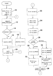
At the start, the variables used in the process are initialized at block 10.
The address
incrementer ADDR, and row counter ROW CTR and column index pointer IDX are set
to 0.
The pre-defined permutation order is stored in a vector named PERM VECT. The
order of
the permuted columns within PERM VECT is preferably as shown in Table 1 for a
FDD
modem receiver 2°d deinterleaver. In step 12, a valve PERM is output
from PERM VECT
based on the IDX value which indicates the column position for the current
element being
processed.
The next several actions 14, 16, 18 determine the number of rows within column
number PERM, and sets the variable NROW to this value. A constant parameter
MAX_COL
is set such that columns 0, 1, 2, .., MAX-COL - 1 have "ROW" number of rows in
them, and
columns MAX COL, ..., C - 1 have "ROW-1" rows in them. Based on this fact and
the
current value of PERM, the variable NROW is set accordingly.
CA 02560715 2001-07-19
-12-
PARAMETER DESCRIPTION
ADDR Word address incrementer in M_INP
for
words W' startin at address Ao
T Total number of elements in data
block
ROW CTR (or n) Counter for counting rows in column
PERM.
PERM VECT Column permutation vector.
COL (or C) Number of columns in permutation
matrix.
ROW (or N) Number of rows in permutation matrix.
PERM (or i) PERM VECT element pointed to by IDX.
IDX PERM_VECT element pointer.
MAX COL Constant value equal to T- (C* (N-1)).
NROW Number of rows in column number PERM.
SA Start bit address of element.
EA End bit address of element
SM Start word address of element.
EM End word address of element.
S Start bit location of element within
SM.
E End bit location of element within
EM.
M Number of bits in each element T'#
or T#.
R, R1, R2 Storage registers.
L' Number of bits in each word of set
W'.
L Number of bits in each word of set
W.
Table 2 - List of Flow Chart Parameters
CA 02560715 2001-07-19
-13-
In steps 20, 22, using the initial address Ao,'the current ADDR value, and the
element
size M, start and end bit-addresses, SA and EA respectively, of the current
data element
within M INP are determined. Dividing SA and EA by the word bit size L' and
discarding
any remainder (or equivalently shifting right by 5) per step 24 generates the
corresponding
word address in the word set W'. These word addresses are SM and EM,
respectively. Then
in step 26, the start and end bit-locations of the data element within the
memory words)
identified by SM and EM is calculated as S and E, respectively. S and E may be
contained
within a single memory word of the set of words W', or be spread across two
consecutive
memory words. The next set of actions 28, 30, 32, 34, 36 demonstrates how
these two
scenarios are handled.
The next action 28 in the flowchart is to compare the SM and EM word
locations. If
the element is within a single word of the set of words W', i.e. EM=SM, then
in step 30, the
word in location SM is fetched from M INP. The element is then, in step 32,
extracted from
its bit locations, as indicated by S and E, and the value is assigned to
register R. If, on the
1 S other hand, the element is contained within two words of the set of words
W', i.e. EM=SM+1,
two words have to be accessed from M INP. Accordingly, the word from SM is
fetched and
assigned to register Rl and the word from EM is fetched and assigned to
register R2 is shown
in step 34. Then in step 36 the bits of the element are extracted from R1 and
R2 and assigned
to register R. Thus, in either case, all of the bits of the interleaved
element contained in the
set of words W' stored in M INP are extracted. Finally, the address counter
ADDR is
incremented for initializing the extraction of the next element.
The next set of actions 40-60, shown in Figure l Ob, is to determine the
words) and bit
location within M LOC where the extracted element will be stored, access the
word(s), place
the element within appropriate bit locations within the word(s), and write the
words) back
into M LOC. These steps can be performed as a single read-modify-write
operation.
The start and end mapping bit addresses, SA and EA, of where the extracted
element
stored in R, in step 32 or 36, will be stored into M LOC is determined in
steps 40-42. The
start address is calculated in step 40 based on the row and element column
mapping of the
element extracted in steps 30, 32 or 34, 36. The matrix position is calculated
by multiplying
the row number, given by ROW CTR, by the number of matrix columns, COL, plus
the
current column number PERM derived from the PERM VECT vector, i.e.
CA 02560715 2001-07-19
-14-
(ROW CTR * COL) + PERM. Since each element has M bits, the result is
multiplied by M
to get SA.
Dividing SA and EA by L, the bit size of the words in set W, and discarding
the
remainder, generates the corresponding word addresses in step 46. These word
addresses are
SM and EM, respectively. Finally, the start and end bit-locations of where the
extracted
element in register R is to be placed are computed as S and E, respectively.
Where L is not
evenly divisible by M, S and E may be contained within a single memory word,
or be spread
across two consecutive memory words of the set of words W. The next set of
actions 48, 60
describe how these two scenarios are handled.
In step 48, the addresses SM and EM are compared. If the extracted element is
to be
stored is within a single word, i.e. SM=EM, then in step 50 the word in
location SM is fetched
from M LOC and placed in register R1. The extracted element value in R is
then, in step 52,
written to the bit locations indicated by S and E within Rl. Finally, Rl is
written back into
memory location SM of M LOC in step 54.
If on the other hand, the extracted element is to be stored within two
consecutive
words having addresses SM and SM+1, those words are fetched in step 56 from M
LOC and
placed in registers R1 and R2, respectively. Then, in step 58, the bits of the
extracted element
within R are placed into appropriate locations in registers R1 and R2,
respectively, based upon
S and E. Finally, the register contents of R1 and R2 are written back, in step
60, into memory
locations SM and SM+1, respectively.
The next action in step 62 is to increment the row counter ROW CTR by 1 to
indicate
that the next extracted element T'# will be stored in the next row of the same
column. A
check is made in step 64 to determine if the row counter is less than or equal
to the number of
rows of the current column, NROW. If that is the case, the process continues
at step 20 with
the next element within column member PERM.
If ROW CTR is not less than NROW, in step 64, the next extracted element will
be
stored at an address corresponding to the first row (row 0) of the next column
indicated by the
vector PERM VECT. Accordingly, if that is the case, ROW CTR is reset to 0 and
the
PERM~VECT index, IDX, is incremented by 1 in steps 66, 68. If, in step 70, IDX
is less than
COL, the deinterleaving process is repeated from step 12 with a new value of
PERM being
CA 02560715 2001-07-19
-15-
assigned, otherwise the process is stopped since all T elements of the data
block will have
been processed.
While the general processing method is described in accordance with the flow
charts
of Figures 10a and l Ob, a preferred implementation of the process in hardware
is illustrated in
Figures l la-l lc. The preferred design consists of a 3-stage pipeline, with
an associated
memory, LOCAL MEMORY, for storing the deinterleaved bits of data. Parallel
processing
components of the first stage are illustrated in Figures l la and l 1b; the
second and third stage
processing is illustrated in Figure l lc.
The operation of stage-1 commences with the extraction of a data element from
a 2L'
bit vector defined by the contents of two registers REG3 and REG4. The
registers REG3 and
REG4 store two consecutive L' bit words from physical channel (PyCH) memory.
For the
preferred 32-bit word size, these two registers form a 64-bit vector of bits.
A register REGO, an adder 71, a substracter 72, and a selector 73, are
configured to
operate in conjunction with a merge device 74 to extract elements having a
size of M bits
from registers REG3 and REG4 on a sequential basis and store the element in a
register
REG2. To initialize the interleaver, first and second words of the sequential
words W' are
initially stored in registers REG3 and REG4, respectively, and register REGO
is initialized to
0. The merge device 74 receives the value 0 from register REGO, extracts the M
bits starting
at address 0 through address M-1. Thus, the first M bit from the initial word
in REG3, which
corresponds to the first element T'0 are extracted. The merge device 74 then
stores the
extracted M bits in the pipeline register REG2.
The value of register REGO is incremented by either M via the adder 71 or M-L'
via
the adder 71 and the substracter 72 based upon the action of the selector 73.
If incrementing
the value of register REGO by M does not exceed L', the selector 73 increments
register REGO
by M. Otherwise, the selector 73 increments the register REGO value by M - L'.
This
effectively operates as a modulo L' function so that the value of REGO is
always less than L'
thereby assuring that the start address of the element extracted by the merge
device 74 is
always within the bit addresses 0 - L' - 1 of register REG3.
Where the selector 73 selects to increment register REGO by M - L', a signal
EN is
sent to trigger the transfer of the contents of REG4 to REG3 and the fetching
of the next
CA 02560715 2001-07-19
-16-
sequential word of the set of words W' from the external memory for storage in
REG4.
During the fetch process, the entire pipeline is stalled. The subtracting of
L' in conjunction
with the incrementing of the value of register REGO corresponds with the
transfer of the word
W' in register REG4 to register REG3 so that the sequential extraction of
elements is
continued with at least the first bit of the element being extracted from the
contents of register
REG3.
With reference to Figure l 1b, an interleaves positioning value is calculated
in parallel
with the extraction process for the element being extracted. The matrix
mapping information
is calculated by retrieving a current row value n from a register N-REG, and
multiplying it in
a multiplier 75 by the number of element columns COL in the interleaves
matrix. An adder
76, then adds a current column value i which is output from a register file 77
containing the
interleaves column sequence as a vector PERM-VECT. The output of the register
file 77 is
controlled by the content of an index register I-REG which increments the
value of the output
of the register file 77 in accordance with the vector PERM VECT.
The matrix mapping circuitry also include elements to selectively increment
the row
index register N-REG and the column index register I-REG. The circuitry
effectively
maintains the same column until each sequential row value has been used and
then increments
the column to the next column in the interleaves vector starting at the
initial row of that
column. This is accomplished through the use of a unit incrementer 80
associated with the
row register N-REG to increment the row value by one for each cycle of first
stage
processing. The output of register N-RBG is also compared in comparator 81
against a
maximum row value determined by a multiplexes 83. The maximum row value for
the
particular column is either the maximum row value ROW of the entire matrix or
ROW-1.
The multiplexes 83 generates an output in response to a comparator 84 which
compares the
column value currently being output by the register file 78 with the largest
column value
having the maximum row size ROW.
If the comparator 81 determines that the maximum row number has been reached
by
the output value of register N-REG, the comparator 81 issues a signal to reset
N-REG to 0 and
to operate a multiplexes (MUX) 86 associated with the index register I-REG. A
unit
incrementer 88 is also associated with the index register I-REG and the MUX 86
permits
incrementation of the I-REG value by one via the incrementer 88 when a signal
is received
CA 02560715 2001-07-19
-17-
from comparator 81. Otherwise, the multiplexes 86 simply restores the same
value to register
I-REG during a first stage cycle.
Refernng to Figure l lc, the second stage of the pipeline interleaves
comprises a
processing cycle where the element extracted and stored in the first pipeline
register REG2 is
transferred and stored into a second data pipeline register REG9. In parallel
in the second
stage of processing, the corresponding matrix mapping data stored in register
REG1 is used to
calculate corresponding start bit address data which is stored in a register
BEGS, end bit
address data which is stored in a register REGB, start word address data which
is stored in a
register REG6, and end word address data which is stored in a register REG7.
During a
second stage cycle, the matrix mapping data from REG1 is initially multiplied
by the element
bit size M in a multiplier 90. The start bit address data is then calculated
by subtracting from
that resultant value in a substracter 91 a value to produce a modulo L
equivalent, where L is
the bit size of the data words of a local memory 100 where the extracted
elements are to be
selectively stored. The value subtracted in substracter 91 is calculated by
dividing the output
1 S of multiplier 90 by L without remainder in divider 92 and multiplying that
value by L in
multiplier 93. The output of the divider 92 also provides the start word
address of the
corresponding word within which at least a first portion of an element in
register REG9 is to
be stored in the local memory 100.
The end bit address data is calculated by adding M-1 to the result of the
multiplier 90,
in an adder 95 and then subtracting from that value in a subtracter 96 a value
calculated to
produce a modulo L value which is then stored in register REG8. The value
subtracted is
derived by dividing the output of the adder 95, in a divider 97, by L without
remainder and
then multiplying the result by L in a multiplier 98. The output of divider 97
also provides the
end word address data which is stored in register REG7.
The third stage of the pipeline interleaves performs a read-modify-write to
selectively
store the element value in register REG9 in the local memory based upon the
data in registers
REGS, REG6, REG7 and REGB. Initially, the contents of registers REG6 and REG7
are
compared in a comparator 99. If the values are equal, the element in register
REG9 will be
stored within a single word of the local memory 100. In that case, the value
from register
REG6 passes through multiplexes 101 to multiplexes 102 where it may be
combined with a
base address which can be used to allocate overall memory resources within the
system.
CA 02560715 2001-07-19
-18-
The output of multiplexer 102 indicates the address of the word W into which
the
element in register REG9 is to be written. That word is output to a de-
multiplexer 103
whereupon a merged device creates a new word comprised of the bit values of
the element in
register REG9 in the sequential addresses within the word starting with the
value in register
REGS and ending with the value in register REGB, with the remaining bits of
the word being
copied from the values of the word in de-multiplexer 103. The newly formed
word in the
merge device 105 is then stored back to the address from which the original
word was output
to the de-multiplexer 103.
Where the contents of registers REG6 and REG7 are different, the first and
second
stages of the pipeline are stalled for one cycle so that the third stage can
perform a read-
modify-write cycle with respect to the word identified by the data in register
REG6 and then
resume the pipeline cycles of all stages to perform a read-modify-write with
respect to the
local memory word corresponding to the end word data stored in register REG7.
In that case,
during the read-modify-write cycle with respect to the word corresponding to
the start word
address data in register REG6, the third stage stores an initial portion of
the element stored in
register REG9 in the last bits of the local memory word starting with the bit
position indicated
by the value stored in register REGS. During a second third stage cycle, where
the first and
second stage cycles are resumed, the remaining portion of the element in
register REG9 is
stored in the word corresponding to the end word address data in register REG7
starting with
the initial bit of that word through the bit address indicated by the value in
register REGB.
After all T elements of a block of data bits have been processed, the
sequential words
of the local memory are read out via the de-multiplexer 103 for further
processing in the
system. The output of the local memory after processing for the 310 element
data block
reflected in the example of Figures 5-8 correspond to the word sequence
reflected in Figure
7c. During further processing within a 3G system, the expanded six bit
elements are
contracted to a single bit thereby, for the example, reproducing the original
310 bit data block
in the same sequence as originally occurnng in the transmitter unit.
Testing of the 3-stage pipeline of the second interleaver was carned out using
two
different techniques. First of these testing methods was a manual technique
called regression.
Regression testing was carried out by fetching 30, 32-bit words from the PyCH
memory,
extracting 6-bit elements from them, and passing them down the pipeline. The
testing cycle
CA 02560715 2001-07-19
-19-
was based on manual cycle-bases simulation, where the expected contents of the
registers and
the internal memory were determined by hand. These values were compared with
the actual
values obtained from simulation. The simulation was carned out for a large
number of test
cases and for all cases of the pipeline stall condition. The interleaves
pipeline was found to
function correctly under all the test scenarios of the manual setting.
Next, the interleaves was independently implemented in C-language. A set of
test
vectors were applied to the C-block and outputs were monitored and written to
a results file.
The same set of input test vectors were applied to the VHDL model. Two sets of
input
vectors were used in the tests:
A 201-element input vector and a 540-element input vector. Two different sets
of
inputs were used to create two different interleaves matrices. The 201-element
matrix had
two different row sizes; one row is one less than the other one. The 540-
element matrix had a
single row size. Thus, the tests included the two different types of
interleaves matrix
structures that are possible. The test results showed that the output vectors
from the VHDL
model and the C-language model matched the two input cases.
The hardware was synthesized using Synopsys Logic Synthesizer, Using Texas
Instruments 0.18um standard cell library. The gate counts are given below.
Number of Standard Cells (TIlGS30/Std-Cell)1034
Sequential gates 1844
Combination gates 3348
Total gates 5192
Table 3 - Total gate count estimate for the interleaves
The pipelined architecture ensures a high-rate of throughput, and a small
compact area
due low number of gates. While a three stage pipeline is preferred, a two
stage design is
easily implemented by eliminating registers REG1 and REG2 from the preferred
system
illustrated in Figures 11 a-11 c.
Other variations and modifications will be recognized by those of ordinary
skill in the
art as within the scope of the present invention.