Note: Descriptions are shown in the official language in which they were submitted.
CA 02560736 2006-09-21
WO 2005/101777 PCT/US2005/011963
-1-
TITLE
APPARATUS FOR AND METHOD OF CONTROLLING A
DIGITAL DEMODULATOR COUPLED TO AN EQUALIZER
CROSS REFERENCE TO RELATED APPLICATIONS
[0001] This application claims the benefit of U. S. Provisional Application
No.
60/561,085, filed April 9, 2004, and entitled "Advanced Digital Receiver" and
further claims
the benefit of U. S. Provisional Application No. 60/601,026, filed August 12,
2004, and
entitled "Advanced Digital Receiver." The present application also
incorporates by reference
U.S. Application Serial No. 10/408,053, filed April 4, 2003, and entitled
"Carrier Recovery
for DTV Receivers," U.S. Application Serial No. 09/875,720, filed June 6,
2001, and entitled
"Adaptive Equalizer Having a Variable Step Size Influenced by Output from a
Trellis
Decoder," (now U.S. Patent No. 6,829,297), U.S. Application Serial No.
10/407,634, filed
April 4, 2003, and entitled "System and Method for Symbol Clock Recovery,"
U.S.
Application Serial No. 09/884,256, filed June 19, 2001, and entitled "Combined
Trellis
Decoder and Decision Feedback Equalizer," and U.S. Application Serial No.
10/407,610,
filed April 4, 2003, and entitled "Transposed Structure for a Decision
Feedback Equalizer
Combined with a Trellis Decoder."
REFERENCE REGARDING FEDERALLY SPONSORED RESEARCH OR
DEVELOPMENT
[0002] Not applicable
SEQUENTIAL LISTING
[0003] Not applicable
CA 02560736 2006-09-21
WO 2005/101777 PCT/US2005/011963
-2-
BACKGROUND OF THE INVENTION
1. Field of the Invention
[0004] The present invention relates generally to digital communication
techniques, and
more particularly, to an apparatus for and method of controlling a digital
demodulator
coupled to an equalizer.
2. Description of the Background of the Invention
[0005] Discrete data transmission is the transmission of messages from a
transmitter to a
receiver through a communication channel. A message sender or sending device,
located at
the transmitter, communicates with a message receiver by selecting a message
and sending a
corresponding signal or waveform that represents this message through the
communication
channel. The receiver determines the message sent by observing the channel
output.
Successive transmission of discrete data messages is known as digital
communication.
Channel noise often interferes with the transmission and degrades the
transmitted message
and leads to some uncertainty as to the content of the original message at the
receiver. The
receiver uses a procedure known as detection to decide which message, or
sequence of
messages, the sender transmitted. Optimum detection minimizes the probability
of an
erroneous receiver decision on which message was transmitted.
[0006] Messages are comprised of digital sequences of bits converted into
electrical
signals that are sent through the channel. These bits are typically encoded
prior to
modulation. Encoding is the process of converting the messages from an innate
form,
typically bits, into values that represent the messages. Modulation is a
procedure for
converting the values into analog signals for transmission through the
channel. The channel
distorts the transmitted signals both deterministically and with random noise.
Those
conditions that interfere with proper reception include additive white
Gaussian noise
(AWGN) and coherent noise, frequency dependent channel distortion, time
dependent
channel distortion, and fading multipath. Because of these effects, there is
some probability
that the sent message is corrupted when it reaches the receiver.
[0007] Upon reception, the receiver demodulates the incoming waveform. In
general,
demodulation attempts to recover the original transmitted signals as
accurately as possible
and converts the recovered signals to estimates of the values. There are
several steps to this
CA 02560736 2006-09-21
WO 2005/101777 PCT/US2005/011963
-3-
process, including downmixing the radio frequency (RF) and near-baseband
intermediate
frequency (IF) signals to the baseband representation, channel equalization,
and decoding.
Symbol and carrier recovery are undertaken so that the discrete time samples
are at the
correct symbol rate and the signal is moved exactly down to baseband. The
receiver employs
a detector to probabilistically determine the value estimates. It is important
that the methods
of demodulating and detecting the received signal as employed by the receiver
consider both
the possible transmitted values and potential for channel-induced errors. The
value estimates
are then decoded by converting the value estimates back into the innate form
of the message.
[0008] Digital communications systems receive the transmitted information by
periodically sampling the output of the demodulator once per symbol interval.
This requires
the receiver design to overcome the problems associated with system
synchronization, as
related to symbol -timing and carrier recovery, under non-ideal transmission
channel
conditions. The optimal times for the receiver to sample the received signal
are generally
unknown due to the propagation delay from the transmitter to the receiver and
the influence
of channel conditions such as multipath. The propagation delay in the
transmitted signal also
results in a carrier phase offset. For those transmission systems requiring a
receiver to
employ a phase-coherent detector, the receiver develops an estimate of the
propagation delay
and derives an estimate of the transmitted symbol timing and phase error
directly from the
received signal. The exception to this is the case where pilot or control
signals are embedded
in the transmitted signal. In such a case, the receiver uses the embedded
pilot or control
signal to synchronize the receiver to the transmitter. In either case, the
receiver overcomes
the system synchronization obstacles by performing three basic functions:
carrier recovery,
timing recovery, and channel equalization.
[0009] As noted above, the carrier recovery process includes a number of steps
whereby
the received radio frequency (RF) signal is demodulated. In part, the near-
baseband signal is
demodulated so as to recover the information-bearing baseband signal and to
remove any
residual carrier phase offset. This final step is often referred to as phase-
locking.
[0010] The timing recovery process is used to recover the transmitter time
base and
synchronize the receiver and transmitter clocks. Once achieved, this
synchronization permits
the receiver to sample the received signal at optimum points in time and
reduce slicing errors.
CA 02560736 2006-09-21
WO 2005/101777 PCT/US2005/011963
-4-
[0011] The channel equalization process attempts to compensate for the
imperfections
within the transmission channel, which change the amplitude and phase of the
received signal
as it traverses the channel. These imperfections are generally frequency
dependent, time
dependent, and dynamic. Because of this, it is advantageous to employ an
adaptive equalizer
filter system to remove the amplitude and phase distortions from the channel.
[0012] There are a number of phase-locked loop (PLL) techniques in existence.
A
limited list of example approaches that will be appreciated by those skilled
in the art, are
Costas loops, squaring loops, and, more generally, decision directed and non-
decision
directed loops.
[0013] Phase-locking mechanisms typically involve three common elements. They
are
phase error detection/generation, phase error processing, and local phase
reconstruction. The
phase error detection operation, as implemented by a phase detector, derives a
phase
difference measurement between the transmitted signal phase, as detected at
the receiver, and
a phase estimate of the incoming signal as developed by the receiver. The
phase error
measurement is the difference between the phase of the received and the actual
transmitted
signal.
[0014] The phase error processing operation, commonly embodied by an
integrator or
low - pass loop filter, extracts the essential phase difference trends by
averaging, over a
period of time or within a time window, the magnitude of the phase error.
Properly designed,
the phase error processing operation rejects random noise and other
undesirable components
of the phase error signal. In order to insure stability, the loop filter
absorbs gain resident in
the phase detector. There are analog, digital and hybrid analog-digital phase
error detection
methods utilized within phase-locked loops. These methods use components
including, but
not limited to, modulo-2~ phase detectors, binary phase detectors, phase-
splitting filters, and
maximum-likelihood carrier phase estimators.
[0015] The local phase reconstruction operation is responsible for controlling
the
generation and phase of a local oscillator. The local oscillator is used to
demodulate the near-
baseband signal with a locally generated oscillator frequency having the same
frequency and
phase as the near-baseband signal. When locked, the resulting local oscillator
signal has the
same frequency and phase characteristics as the signal being demodulated to
baseband. The
CA 02560736 2006-09-21
WO 2005/101777 PCT/US2005/011963
-5-
local oscillator may be implemented using either analog or digital means.
Various types of
voltage controlled crystal oscillators and numerically controlled oscillators,
VCXO's anel
NCO's, respectively, may be used to regenerate the local carrier.
[0016] In the case of an analog circuit, the local phase reconstruction
operation is
implemented using a voltage-controlled oscillator. The VCXO uses the processed
phase
error information to regenerate the local phase of the incoming signal by
forcing the phase
error to zero.
[0017] Any phase-locking mechanism has some finite delay in practice so that
the
mechanism attempts to predict the incoming phase and then measures the
accuracy of that
prediction in the form of a new phase error. The more quickly the phase-lock
mechanism
tracks deviations in phase, the more susceptible the mechanism is to random
noise and other
imperfections. This is all the more the case where the received signal exists
in a strong
multipath environment. Thus, an appropriate trade-off is made between these
two competing
effects when designing a synchronization system.
[0018] Timing recovery, or synchronization, is the process whereby a receiver
synchronizes the local time base thereof to the transmitter symbol rate. This
allows for
precise sampling time instants during the symbol period so as to maximize the
likelihood of
correctly determining the value of the transmitted symbol. As previously
described, the PLL
subsystem is insufficient to recover the symbol rate. Instead, a separate
symbol-timing
recovery function is added in combination with the PLL to provide timing
recovery.
Improper symbol-timing recovery is one source of intersymbol interference
(ISI) and
significantly degrades the performance of the receiver.
[0019] As those skilled in the art W 11 appreciate, proper sampling of the
demodulator
output is directly dependent upon proper timing recovery. There are a number
of methods
utilized by systems to perform local clock recovery. In a first system,
various types of
clocking signals are encoded into the bit stream. In a second system, no
predefined
synchronization symbols are transmitted and only data are sent and the locked
local clock is
derived from the received data stream. It should be noted that the latter
system appears to be
more prevalent due to the desire for bandwidth efficiency.
CA 02560736 2006-09-21
WO 2005/101777 PCT/US2005/011963
-6-
[0020] In addition, timing recovery methods are also distinguishable as to
their use of the
decision device output of the receiver. A non-decision aided methodology does
not depend
upon the output of the decision device. An example of such a methodology is
the square-law
timing recovery method. Also, envelope-timing recovery is an equivalent squaxe-
law timing
recovery method utilized in a Quadrature Amplitude Modulation (QAM) receiver.
[0021] Decision directed (also known as decision-aided) timing recovery uses
the
decision device output. One example of a decision directed timing recovery
method
minimizes the mean-square error, over the sampling time phase, between the
output of either
a linear equalizer (LE) or a decision feedback equalizer (DFE) and the
decision device
output.
[0022] The decision device is responsible for assigning a symbol value to each
sample
obtained from the demodulator. There are both hard and soft decision devices.
An example
of a hard decision device is a decision slicer or a Viterbi decoder. In the
case of decision
directed timing recovery methods, care is taken to ensure that there is not
excessive delay
between the decision device output and the input sampling function. Excessive
delay
degrades the overall performance of the receiver or, in the worst-case, causes
the phase-
locked loop to become unstable. As will be appreciated by those skilled in the
art, the quality
of the symbol-timing estimates is dependent upon the overall signal-to-noise
ratio (SNR) and
is a function of the signal pulse shape and the channel characteristics.
[0023] There are numerous sources of channel distortion and interference that
may result
in poor receiver performance, as measured by either bit error rate (BER) or
overall data
transfer rates of a receiver design. Factors include noise, AWGN, inter-symbol
interference
(ISI) and multipath conditions.
[0024] Receivers also compensate for channels having significant multipath
characteristics. There are various means of classifying or describing
multipath phenomenon,
depending upon the channel frequency response and time varying multipath
effects. Four
common categorizations, familiar to those skilled in the art, are slow
changing frequency
non-selective fading, fast changing frequency-non selective fading, slow
changing frequency
selective fading, and fast changing frequency selective fading.
CA 02560736 2006-09-21
WO 2005/101777 PCT/US2005/011963
_7_
[0025] Typically, multipath is the result of the transmitted signal arriving
at the receiver
via different transmission paths, each having a unique composite propagation
time to the
receiver. The multipath induced ISI results in the receiver contending with
non-constant
amplitude and non-linear phase response of the channel. Tha second effect is
referred to as
fading. Fading is due to the propagation delay associated with each
propagation path
resulting in constructive and destructive interference at the receiver. Fading
causes
degradation of SNR.
[0026] This simplistic description is further refined into four categories,
familiar to those
skilled in the art, as summarized by the practical implications thereof. In
practice, a channel
exhibiting slowly changing, frequency non-selective fading means that all of
the propagation
paths are received within one symbol period and that the channel equally
affects all the signal
frequency components. This is considered the most easily compensated fading
channel
phenomenon. Fast changing, frequency non-selective fading arises where the
channel varies
during the symbol period. Fast fading is very difficult to compensate
effectively.
[0027] A channel may be characterized as having slow, frequency-selective
multipath
when the channel distorts the received symbol in the frequency domain and not
all the
frequency components are equally affected. As a consequence, the baseband
pulse shape is
distorted and intersymbol interference results. Finally, fast changing,
frequency-selective
fading is considered the worst-case type of channel, and resulta when the
received symbol is
spread over many symbol periods and the channel characteristics also vary
during the symbol
period.
[0028] Fading is also roughly divided into large- and small-scale fading
categories as
shown in FIG. 1. Large motions of the receiver, such as occur in mobile
applications, cause
large-scale fading, whereas small-scale fading is due to motion of the
receiver. Large-scale
fading is also called log-normal fading, because the amplitude thereof has a
log-normal
probability density function. Small-scale fading is usually described as
Rayleigh- or Ricean-
fading, depending on which probability distribution function (pdf) best
describes it. In
addition, a Nakagami-m distribution has also been used to characterize some
multipath
channel conditions.
CA 02560736 2006-09-21
WO 2005/101777 PCT/US2005/011963
_g_
[0029] Many modern digital communications systems employ adaptive equalization
to
compensate for the effects of changing conditions and disturbances in the
signal transmission
channel. Equalization is used to remove the baseband inter-symbol interference
caused by
transmission channel distortion and may be performed on baseband or passband
signals.
Equalization is often performed on the near-baseband signal prior to carrier
recovery and the
down mixing to produce a baseband signal. This is particularly the case in a
decision
directed carrier recovery process, as will be appreciated by those skilled in
the art, which
requires at least a partially open eye.
[0030] A representation of an 8-VSB, vestigial sideband, eye diagram is shown
in FIG. 2.
The eye diagram is the overlay of many traces of the received RF signal
amplitude at the
instant of sampling. The convergence of the many signal traces forms seven
"eyes" that
coincide with the occurrence of clock pulses in the receiver. At each sampling
time, the
demodulated RF amplitude assumes one of eight possible levels. If the 8-VSB
signal is
corrupted during transmission, these "eyes" will close up and disappear, as
the RF signal will
no longer possess the correct amplitude at the right instant.
[0031] An adaptive equalizer filter system is essentially an adaptive digital
filter having a
modifiable frequency and phase response that compensates for channel
distortions. As will
be appreciated by those skilled in the art, several architectures, methods and
algorithms are
available to implement this function. In one embodiment, a feed-forward
equalizer (FFE)
develops a partially equalized signal that is provided to a decision feedback
equalizer (DFE).
In typical systems of this type, the FFE is responsible for minimizing or
eliminating ghosts
resulting from precursor inter-symbol interference (ISI) while the DF~ is
responsible for
minimizing or eliminating ghosts resulting from postcursor ISI. In another
system, the FFE
reduces or eliminates ghosts due to precursor and some postcursor ISI wLzile
the DFE reduces
or eliminates ghosts resulting from postcursor ISI.
[0032] The impact on receiver performance of multipath induced ISI is reduced
by the
application of channel estimation and equalization. The effectiveness of the
channel estimate
has a direct relationship to elimination of ISI. An ideal channel estimate, in
theory, would
allow complete removal of the ISI. Obtaining an ideal channel estimate,
however, is
problematic when presented with particularly odious channel characteristics.
CA 02560736 2006-09-21
WO 2005/101777 PCT/US2005/011963
-9-
[0033] Another approach to improving performance in the preserice of multipath
interference is based on the diversity principle. The different propagation
paths are used in
combination to mitigate the multipath fading. This is possible because the
propagation paths
are usually not correlated, meaning it is unlikely that all of them fade
simultaneously. The
diversity concept models the channel fading mechanism as a channel burst
error. Thus,
providing temporally or frequency-based redundant copies of the transmitted
information
improves the likelihood of successful data transmission.
[0034] Diversity techniques include temporal diversity and frequency
diversity.
Frequency diversity requires that the same information be transmitted over a
number of
carriers where the spacing of successive carriers equals or exceeds the
coherent bandwidth of
the information channel. Temporal diversity employs the use of a number (L) of
independently fading versions of the same information-bearing signal
transmitted into L
different time slots, where the separation between successive time slots
equals or exceeds the
coherence time of the channel. Thus, L copies of the transmitted information
are presented to
the receiver at varying times based on the transmission path.
[0035] One realization of this concept is a Rake Receiver. The Rake Receiver
exploits
the multipath phenomenon to improve system performance. Multiple basaband
correlators
are used to individually process multiple multipath components. The correlator
outputs are
then added to increase total signal strength.
[0036] The above characterizations are intended only as a partial, non-
limiting list of
example techniques that may be employed and are not intended in any way to
represent any
limitation upon the disclosed invention.
[0037] Despite the numerous techniques available in the present state of the
art, receivers
exhibit significant performance degradation in the presence of strong
multipath
environments. This is particularly true in the case of terrestrial digital
broadcasting systems.
In particular, the present state of the art receiver using an equalizer
typically uses subtractive
methods to remove interfering multipath signals. This has a distinct
disadvantage in a
changing multipath fading environment. In particular, these receiver systems
attempt to
identify and lock onto the single strongest received signal coming through a
given
transmission path or channel. This is accomplished at start up of the
equalizer by establishing
CA 02560736 2006-09-21
WO 2005/101777 PCT/US2005/011963
-10-
a tap of unity magnitude at a center point of the FFE. Upon reception, signals
correspondirig
to other transmission paths are subtractively removed from the incoming total
signal. This
effectively removes all diversity from the receiving process (if diversity is
used in tt-~e
system). Also, the receiver can lose lock as the strength of the primary
multipath signal fades
or a new stronger signal appears. This introduces significant carrier phase
offset at the
receiver. Changing multipath conditions thus often necessitate a receiver to
reacquire carrier
lock, resulting in a possibly noticeable disruption in information flow to a
user at the receive.
SUMMARY OF THE INVENTION
[0038] According to one aspect of the invention, a method of controlling a
digital
demodulator coupled to an equalizer includes the steps of generating an
equalizer value,
filtering the equalizer value to obtain a post filter output, and subtracting
the equalizer output
signal from decoded data and generating an error value. The post filter output
is correlated
with the error value to obtain a correlated value. A control signal is
developed from the
correlated value and is used to adjust the digital demodulator.
[0039] According to another aspect of the present invention, a post filter for
controlling a
digital demodulator coupled to an equalizer includes means for generating an
equalizer vale
and means for filtering the equalizer value to obtain a post filter output.
The post filter
further includes means for subtracting an equalizer output signal from decoded
data arid
generating an error value and means for correlating the post filter output
with the error value
to obtain a correlated value. Further means are also provided for developing a
control signal
from the correlated value and means for adjusting the digital demodulator
using the control
signal.
[0040] According to yet another aspect of the present invention, a computer-
readable
medium for controlling a digital demodulator coupled to an equalizer includes
programming
for implementing multiple routines. A first routine generates an equalizer
value and a second
routine filters the equalizer value to obtain a post filter output. A third
routine subtracts an
equalizer output signal from decoded data and generates an error value. A
fourth routine
correlates the post filter output with the error value to obtain a correlated
value. A fifth
CA 02560736 2006-09-21
WO 2005/101777 PCT/US2005/011963
-11-
routine develops a control signal from the correlated value and a sixth
routine adjusts the
digital demodulator using the control signal.
[0041] Other aspects and advantages of the present invention will become
apparent upon
consideration of the following detailed description.
BRIEF DESCRIPTION OF THE DRAWINGS
[0042] FIG. 1 is a graph showing the relationship between small- and large-
scale fading
over time;
[0043] FIG. 2 is a graph showing an eight-VSB modulated open eye pattern;
[0044] FIG. 3 is a schematic block diagram of an advanced digital receiver
according to
the present invention;
[0045] FIG. 4 is a diagram of the ATSC baseband framing code segment format
showing
the data segment and frame sync structure;
[0046] FIG. 5 is a schematic of one embodiment of an equalizer for use in the
advanced
digital receiver of FIG. 3;
[0047] FIG. 6 is a block diagram of one embodiment of a segment sync based
channel
delay estimation unit (CDEU);
[0048] FIG. 7 is a diagram showing the relative position of a virtual center
relative to
ghosts detected in a transmission channel;
[0049] FIG. 8 is a diagram showing the relative positions of ghosts detected
in a
transmission channel;
[0050] FIG. 9 is a block diagram of one embodiment of an ATSC segment sync
correlator;
[0051] FIG. 10 is a block diagram of one embodiment of a "leaky" integrator;
[0052] FIG. 11 is a block diagram of one embodiment of a centroid estimator;
[0053] FIG. 12 is a flow diagram illustrating operation of a CDEU;
CA 02560736 2006-09-21
WO 2005/101777 PCT/US2005/011963
-12-
[0054] FIG. 13 is a block diagram of another embodiment of a segment sync
based
CDEU;
[0055] FIG. 14 is a block diagram of an embodiment of a frame sync based CDEU;
[0056] FIG. 15 shows the location of ghost signals in a transmission channel
relative to
windowing functions;
[0057] FIG. 16 is a flow diagram illustrating operation of a further
embodiment of a
CDEU;
[0058] FIG. 17 shows the location of ghost signals in a transmission channel
relative to
windowing functions;
[0059] FIG. 18 is a block diagram of another embodiment of a frame sync based
CDEU;
[0060] FIGS 19A-19D show the relationship between the virtual center of the
virtual
channel, FFE output (ZouT), and the FFE and DFE taps and coefficients;
[0061] FIGS. 20A and 20B show the relationship between the virtual center of
the virtual
channel, FFE output (ZouT), and the FFE and DFE taps;
[0062] FIG. 21 is a flow diagram illustrating operation of the system 20 of
FIG. 3 for
developing an overlapped equalizer structure or an equalizer without a fixed
center tap;
[0063] FIG. 22 is a block diagram of an embodiment of an overlapped equalizer
with a
phase tracker;
[0064] FIG. 23 is a block diagram of an embodiment of an overlapped equalizer
with a
phase tracker;
[0065] FIG. 24 is a block diagram of an embodiment of an overlapped equalizer
with a
phase tracker;
[0066] FIG. 25 is a block diagram of an embodiment of an overlapped equalizer
with a
phase tracker;
[0067] FIG. 26 is a block diagram of an embodiment of an overlapped equalizer
with a
phase tracker;
CA 02560736 2006-09-21
WO 2005/101777 PCT/US2005/011963
-13-
[0068] FIG. 27 is a block diagram of an embodiment of an overlapped equalizer
with a
phase tracker;
[0069] FIG. 28 is a block diagram of an embodiment of an overlapped equalizer
with a
phase tracker;
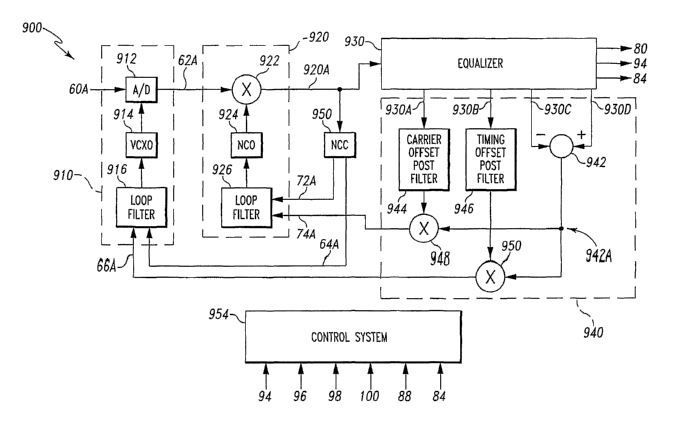
[0070] FIG. 29 is a block diagram of an embodiment of a synchronization and
demodulation feedback system employing an overlapped equalizer;
[0071] FIG. 30 is a flow diagram illustrating operation of another embodiment
of the
system 900 of FIG. 29 for controlling the operation of an overlapped equalizer
optimization
process and synchronization and demodulation control feedback loops;
[0072] FIG. 31 is a block diagram of a further embodiment of a synchronization
and
demodulation feedback system employing an overlapped equalizer;
[0073] FIG. 32 is a block diagram of an embodiment of an overlapped equalizer
within a
combined demodulation and synchronization feedback loop;
[0074] FIG. 33 is a block diagram of an embodiment of an overlapped equalizer
within a
combined demodulation and synchronization feedback loop;
[0075] FIG. 34 is a block diagram of an embodiment of an overlapped equalizer
within a
combined demodulation and synchronization feedback loop;
[0076] FIG. 35 is a block diagram of an embodiment of an overlapped equalizer
within a
combined demodulation and synchronization feedback loop;
[0077] FIGS. 36A and 36B show qualitative characteristics of a timing offset
post filter
and carrier offset post filter, respectively;
[0078] FIG. 37 is a block diagram of an embodiment of a fieldlframe sync
correlation
directed control system for controlling a VCXO in a digital receiver system;
[0079] FIGS. 38A-38C show a relationship of a correlation weighting function
to location
of ghost signals in the channel;
[0080] FIG. 39 is a block diagram of an embodiment of a correlation directed
synchronization feedback system;
CA 02560736 2006-09-21
WO 2005/101777 PCT/US2005/011963
-14-
[0081] FIG. 40 is a flow chart describing operation of an embodiment of a
correlation
directed synchronization feedback loop system;
[0082] FIG. 41 is a block diagram of an embodiment of a system producing a
segment
sync based correlation directed control signal;
[0083] FIG. 42 is a flow chart describing operation of an embodiment of a
system for
generating a segment sync base correlation directed control signal;
[0084] FIG. 43 is a block diagram of an embodiment of a segment sync based
correlation
directed carrier tracking feedback loop; and
[0085] FIG. 44 is a block diagram of an embodiment of a channel delay directed
synchronization feedback loop.
DETAILED DESCRIPTION OF THE PREFERRED EMBODIMENTS
[0086] For the purposes of promoting an understanding of the principles of the
invention,
reference will now be made to the embodiments illustrated in the drawings and
specific
language will be used to describe the same. It will nevertheless be understood
that no
limitation of the scope of the invention is thereby intended. Any alterations
to and further
modification of the described embodiments, and any further applications of the
principles of
the invention as described herein are contemplated as would normally occur to
one skilled in
the art to which the invention relates.
[0087] One aspect of the present system illustrated in FIG. 3 is a digital
receiver system
with significantly improved stability and performance when receiving modulated
signals in
severe multipath environments. The techniques, devices, and systems embodied
in this new
digital receiver may be adapted to various modulation formats, including, but
not limited to,
QAM, offset-QAM and VSB. Illustratively, one non-limiting example transmission
standard
of interest is the ATSC standard adopted for HDTV broadcast in the United
States. The
ATSC transmission standard utilizes a suppressed carrier 8-VSB signal having a
pilot signal
at the suppressed carrier frequency for use in achieving carrier lock in a VSB
receiver. As
shown in FIG. 4, the ATSC data transmission format comprises two fields per
frame. Each
field has 313 segments consisting of 832 multilevel symbols. Each segment has
a four
CA 02560736 2006-09-21
WO 2005/101777 PCT/US2005/011963
-15-
symbol segment sync character followed by a payload of 828 symbols. The first
segment of
each field contains a field sync segment while the remaining segments are used
to transport
data packets. The field sync is characterized by a predetermined 511 symbol
pseudorandom
number (PN) sequence and three predetermined 63-symbol long (PN) sequences.
The middle
63-symbol long (PN) sequence is inverted in each successive field. A VSB mode
control
signal (defined in the VSB constellation size) follows the last 63 PN
sequence, which is
followed by 92 reserved symbols and 12 symbols copied from the'previous field.
It will be
understood by those skilled in the art that the present invention is adaptable
to other
transmission standards without undue experimentation.
[0088] One embodiment of the present invention is system 20, shown in FIG. 3.
System
20 receives and processes an ATSC broadcast signal and includes an analog
front end
receiver 30, synchronization 40, digital demodulator 42, Nyquist Root Filter
(NRF) 44,
equalizer 46, forward error correction (FEC) 48, non-coherent control (NCC)
50, decision
directed control (DDC) 52 and control system 54. Further embodiments of system
20 also
detect the presence of a segment sync, fieldlframe sync, and the signal-to-
noise ratio, SNR, at
various points in system 20. Illustratively, some embodiments of system 20
determine the
SNR of the received data. Other embodiments determine the SNR of the received
signal
based on the received synchronization signals. Certain other embodiments
quantify
performance of the equalizer based upon the data error rate. Similarly, other
elements of
system 20 also use a data error rate to quantify the performance thereof.
Still other
embodiments, also use performance metrics developed by the trellis decoder in
the equalizer
as described in U.S. Patent No. 6,829,297.
[0089] Some embodiments of system 20 also detect a frame or field sync signal
in one of
the outputs of equalizer 46. Other embodiments of system 20 determine whether
the
synchronization 40 or digital demodulator 42 is locked to the received signal.
[0090] The control system 54 connects (not shown) to the various elements of
system 20
and generally directs the function of system 20. Illustratively, in some
embodiments, control
system 54 oversees system startup, operational mode selection, and adaptation
of equalizer
coefficients_ As described later, control system 54 receives a channel delay,
estimate 84
(CDE), equalizer output 88, and adaptation symbol decision 94. Control system
54 also
receives signals segment sync 96, fieldlframe sync 98, SNR 100, VCXO lock 102,
and NCO
CA 02560736 2006-09-21
WO 2005/101777 PCT/US2005/011963
-16-
lock 104. Segment sync 96 is a signal indicating that a valid segment sync was
detected at a
desired output of equalizer 46 or other elements of system 20. Field/frame
sync 98 is a signal
indicating that a valid field/frame sync was detected at a desired output of
equalizer 46 or
other elements of system 20. Similarly, SNR 100 is an estimated SNR of the
received signal
at a desired output of equalizer 46. VCXO lock 102 is a signal indicating that
synchronization 40 has locked to the time base of the incoming signal.
Finally, NCO lock
104 is a signal indicating the digital demodulator 42 is locked to the
incoming carrier.
[0091] The input of analog front end receiver 30 connects to an antenna or
other signal
source receiving a broadcast signal. The analog front end receiver 30 tunes to
a desired RF
broadcast signal, provides automatic gain control (AGC) and signal
amplification, and
converts the received signal to an intermediate frequency (IF) to be used in
the demodulation
process. The analog front end receiver 30 may include RF tuning circuits, IF
circuitry, and
automatic gain control circuitry to optimize the received signal in the
presence of noise.
Analog front end receiver 30 also down-converts the received signal into a
near-baseband
signal. Illustratively, the received lF passband signal of a near-baseband
carrier suppressed
8-VSB signal adopted in the ATSC standard may be roughly centered at 5.38
MFiz.
[0092] In accordance with the present invention, synchronization 40 is part of
the overall
timing recovery function responsible for sampling the incoming signal and
synchronizing
system 20 to the time base of the incoming signal. Synchronization 40 receives
an analog
near-baseband signal 60 from analog front end receiver 30, and produces a
digitized near-
baseband signal 62. Synchronization 40 also receives decision directed
synchronization
feedback signal 66 from decision directed control 52, and a non-coherent
synchronization
feedback signal 64 from non-coherent control 54.
[0093] 1n some embodiments of the present invention, the synchronization 40
includes an
A/D converter (not shown) sampling the incoming analog near-baseband signal 60
to produce
a digital near-baseband signal 60 based on a sample clock produced by a
feedback-controlled
VCXO. Control system 54 controls synchronization 40 to select either decision
directed
synchronization feedback signal 66 or non-coherent synchronization feedback
signal 64 to
control the phase and frequency of the A/D sample clock. In other embodiments,
synchronization 40 also receives a correlation directed control feedback
signal (not shown).
CA 02560736 2006-09-21
WO 2005/101777 PCT/US2005/011963
-17-
The selected feedback signal is filtered to produce a control signal that
governs the VCXO
output frequency and phase.
[0094] Illustratively, in certain embodiments control system 54 initially
configures
synchronization 40 to use non-coherent synchronization feedback signal 64 to
govern the
VCXO operation. The analog near-baseband signal 60 is sampled by
synchronization 40
based on the feedback-controlled VCXO sample clock. After system 20 has at
least partially
converged, control system 54 selectively configures synchronization 40 to use
decision
directed synchronization feedback signal 66 to govern the VCXO operation.
Illustratively,
some embodiments of synchronization 40 adapted for an ATSC system include a
VCXO
driving A/D sampling at a rate of approximately 21.52 MHz, which is twice the
symbol rate
of the received signal in an ATSC system. After the VCXO has locked to the
time base of
the received signal, control system 54 receives a positive indication from
VCXO Lock 102.
It will be appreciated that there are numerous techniques available to those
skilled in the art
for determining whether a VCXO is locked to an incoming signal.
[0095] In other embodiments, the synchronization 40 re-samples the output of a
fixed
sampling rate A/D. Illustratively, an A/D samples the incoming signal 60 at a
fixed rate. The
sample rate converter re-samples the digitized near-baseband signal to develop
a desired
output sample rate that is synchronized to the incoming symbol rate. Similar
to that
discussed above, control system 54 selectively controls the re-sampling
process using either
non-coherent synchronization feedback signal 64 or decision directed
synchronization
feedback signal 66 based on the operational state of system 20.
[0096] Digital demodulator 42 is part of the overall carrier tracking and
recovery function
of system 20 and demodulates the near-baseband output of synchronization 40 to
baseband.
As shown in FIG. 3, the digital demodulator 42 receives the digitized near-
baseband signal 62
from synchronization 40, a decision directed carrier tracking feedback signal
74 from
decision directed control 52, and non-coherent carrier tracking feedback
signal 72 from non-
coherent control 50. Although not shown, other embodiments of digital
demodulator 42 also
receive a correlation directed control feedback signal. According to one
embodiment, the
digital demodulator 42 digitally down modulates the near-baseband signal 62 to
a two times
over-sampled complex baseband output having an in-phase component signal 68
and
quadrature component signal 70. Prior to filtering steps, discussed later, the
in-phase
CA 02560736 2006-09-21
WO 2005/101777 PCT/US2005/011963
-18-
component signal 68 and quadrature component signal 70 have both negative and
positive
frequency components. The output of digital demodulator 42 is lowpass-filtered
by Nyquist
Root Filter 44 to remove out-of band signals.
[0097] As explained later, control system 54 selectively controls the feedback
signal
governing the operation of digital demodulator 42. During initial system
startup, digital
demodulator 42 operation is governed by a non-coherent carrier tracking
feedback signal
from NCC 50. The NCC 50 tracks the received carrier frequency and governs the
down mix
frequency produced by a NCO portion of the digital demodulator. After system
20 is at least
partially converged, control system 54 configures digital demodulator 42 to
utilize the
decision directed controlled feedback loop signal to provide improved carrier
tracking and
governs the down conversion process. At some desired point of digital
demodulation
operation, NCO Lock 104 indicates to control system 54 that the NCO is locked
to the carrier
of the received signal.
[0098] In some embodiments of the present invention, only the in-phase
component
signal 68 is used by the equalizer 4.6 to reduce the complexity of the system.
Alternatively,
other embodiments of the present invention utilize the over-sampled baseband
signal in
conjunction with a fractionally spaced FFE incorporated into equalizer 46 of
system 20.
[0099] Demodulator 42 provides in-phase component signal 68 and quadrature
component signal 70 as inputs to both NRF 44 and NCC 50. NRF 44 filters out
the high
frequency components from the demodulated signal to produce a filtered in-
phase baseband
signal (IF) 76 and filtered quadrature baseband signal (QF) 78 as inputs to
equalizer 46. In
some embodiments, NRF 44 is a low-pass filter with a 5.38 MHz double-sided
bandwidth
and 11 % rolloff.
[00100] As described in inventor's co-pending applications, US Application No.
10/408,053 entitled "Carrier Recovery for DTV Receivers" and U.S. Application
No.
10/407,634 entitled "System and Method for Symbol Clock Recovery" herein
incorporated,
NCC 50 utilizes the pilot signal and redundant information on the upper and
lower Nyquist
slopes to develop a non-coherent carrier tracking feedback signal and a non-
coherent symbol
timing synchronization signal. As mentioned earlier, NCC 50 provides the non-
coherent
CA 02560736 2006-09-21
WO 2005/101777 PCT/US2005/011963
-19-
carrier tracking feedback signal 72 as an input to the digital demodulator 42
and the non-
coherent synchronization feedback signal 64 as an input to synchronization 40.
[00101] As illustrated in FIG. 3, equalizer 46 receives the baseband component
signal IF
76 and QF 78 from the NRF 44. In some embodiments, equalizer 46 utilizes IF 76
and QF 78.
In other embodiments, equalizer 46 only utilizes IF 76, also referred to as
the real component
of the demodulated signal.
[00102] Some embodiments of equalizer 46 establish and update coefficients
using feed
forward techniques, while others use feedback techniques such as LMS fitting.
Certain
embodiments estimate the channel delay as part of this process. Equalizer 46
provides
control system 54 with the CDE 84. Control system 54 then directs the
equalizer coefficient
adaptation process through an LMS algorithm to develop a virtual channel
response that
creates a stable received signal by advantageously combining a multiplicity of
received ghost
signals.
[00103] In other embodiments, equalizer 46 includes a trellis decoder
integrated into the
equalizer structure. In some embodiments the output of the trellis decoder is
used to update
the data samples in the equalizer DFE or direct the equalizer coefficient
adaptation process on
an ongoing basis. In other embodiments, intermediate trellis decoder stage
outputs are used
to direct the equalizer. Still other embodiments, as shown in U. S. Patent
Application No.
10/407,610, entitled "Transposed Structure for Decision Feedback Equalizer
Combined with
Trellis Decoder", include a combined DFE-trellis decoder structure. In yet
further
embodiments, as shown in U.S. Patent Application No. 09/884,256, outputs from
intermediate stages of a trellis encoder are coupled via a mapper to inputs of
certain stages of
the DFE.
[00104] As described herein, equalizer 46 includes techniques for estimating
the channel
delay of the transmission channel through which the information-bearing signal
is
transmitted. Equalizer 46 provides control system 54 with the CDE 84, which is
used in
conjunction with other equalizer adaptation techniques to evolve the tap
coefficients of
equalizer 46. Control system 54 uses the CDE 84 to align the equalizer
relative to the
channel. The CDE 84 is developed from an estimate of the channel impulse
response (CIR).
Some embodiments estimate the CIR by correlating sync signal arrivals. Certain
CA 02560736 2006-09-21
WO 2005/101777 PCT/US2005/011963
-20-
embodiments use the field/frame sync signal. Other embodiments use a segment
sync signal.
Still other embodiments utilize both segment sync and frame sync to train the
coefficients of
equalizer 46. In addition, other embodiments estimate the CIR by correlating
other signals
within the received signal.
[00105] Some embodiments of equalizer 46 have no center tap or reference tap.
This
advantageously allows the equalizer to remain stable even when a multipath
ghost
significantly diminishes the main received signal. Other embodiments include
an overlapped
equalizer with ~a virtual center output. In an overlapped equalizer, some
samples contained in
the FFE and DFE portions of equalizer 46 are temporally related. The
overlapped equalizer
structure permits the virtual center to be strategically placed within the
equalizer to minimize
the effect of noise and improve overall performance. In addition, some
embodiments of
equalizer 46 also include a decision directed phase tracker to remove any
residual phase noise
not eliminated by the digital demodulator 42. Certain of these embodiments
also include
techniques for linking the operation of the decision directed carrier tracking
feedback signal
74 to the operation of the decision directed phase tracker.
[00106] As illustrated in FIG. 3, in some embodiments of system 20, equalizer
46 provides
to decision directed control 52 a synchronization symbol decision 86 and a
corresponding
equalized data signal 88. As described herein, the equalized data signal 88 is
the data signal
provided to the decision device (not shown) of the equalizer. The
synchronization symbol
decision 86 is the value produced by a decision device within the equalizer.
In some
embodiments, the synchronization symbol decision 86 is the output of a
decision dicer. In
other embodiments the synchronization symbol decision 86 is the output from a
selected
stage of a trellis decoder. In certain embodiments of the present invention
equalizer 46
provides to decision directed control 52 an intermediate equalized signal 90
corresponding to
the synchronization symbol decision 86. As described later, in some
embodiments
intermediate equalized signal 90 comes from the output of an FFE. In other
embodiments,
intermediate equalized signal 90 is the phase-corrected FFE output.
[00107] In some embodiments, adaptation symbol decision 94 is a known training
signal,
such as a generated synchronization signal. In other embodiments adaptation
symbol
decision 94 is the output of a decision slicer of equalizer 46. In certain
embodiments,
adaptation symbol decision 94 is the output of a trellis decoder of equalizer
46 or an
CA 02560736 2006-09-21
WO 2005/101777 PCT/US2005/011963
-21-
intermediate state or other stage of the trellis decoder. In still other
embodiments, adaptation
symbol decision 94 depends upon the operational state of system 20 or
equalizer 46.
[00108] Decision directed control 52 generates decision directed carrier
tracking feedback
signal 74 and decision directed synchronization feedback signal 66. The
decision directed
carrier tracking feedback signal 74 is a decision weighted carrier tracking
error estimate for a
particular received symbol. Similarly, the decision directed synchronization
feedback signal
66 represents a decision weighted timing error estimate for a received symbol.
[00109] The input of FEC 48 receives the FEC symbol decision SO of equalizer
46. The
FEC performs a number of post signal processing steps to correct for errors
contained in the
received data. Illustratively, the FEC 48 performs frame synchronization, data
de-
interleaving, and Reed-Solomon forward error correction.
[00110] One embodiment of equalizer 46, illustrated as equalizer 200 in FIG.
5, receives
as inputs filtered in-phase baseband signal (IF) 76 and filtered quadrature
baseband signal
(QF) 78, and provides as outputs FEC symbol decision 80, synchronization
symbol decision
86, equalized data signal 88, intermediate equalized signal 90, and adaptation
symbol
decision 94. As explained herein, some embodiments of equalizer 200 do not
process QF.
[00111] Equalizer 200 further includes a feedforward equalizer (FFE) 210,
adder 212,
decision device 214, DFE 216, and control system 54. As illustrated in FIG. 5,
in some
embodiments of equalizer 200, FFE 210 receives as an input the filtered in-
phase baseband
signal 76. Although not shown in FIG. 5 for the sake of clarity, some
embodiments of FFE
210 also receive QF. The output of FFE 210 provides intermediate equalized
signal 90 to the
first input of adder 212. The output of DFE 216 provides the second input of
adder 212. The
output of adder 212 is equalized signal 88, which serves as the input to
decision device 214.
Although not shown, control system 54 connects to the various elements of
equalizer 200,
governs the operation of equalizer 200, and adapts the coefficients of FT'E
210 and DFE 216.
The FFE is one of a class of filters known in the art that includes
feedforward filters (FFF's)
and finite impulse response (FIR) filters and it would be apparent to one of
ordinary skill in
the art to use an FFF or a FIR filter as an appropriate substitute for the FFE
as used herein.
[00112] As illustrated in FIG. 5, decision device 214 provides a variety of
outputs
including FEC symbol decision 80, synchronization symbol decision ~6,
equalizer feedback
CA 02560736 2006-09-21
WO 2005/101777 PCT/US2005/011963
_22_
symbol output 92, and adaptation symbol decision 94. Equalizer feedback symbol
output 92
is the decision device output provided to DFE 216. FEC symbol decision 80 is
the final
output of equalizer 200 provided to FEC 48, while synchronization symbol
decision 86 is
provided to decision directed control 52 (see FIG. 3). In some embodiments,
synchronization
symbol decision 86 is the output of a decision sficer circuit. In other
embodiments,
synchronization symbol decision 86 is obtained from the output or a selected
stage of a trellis
or Viterbi decoder. In still other embodiments, synchronization symbol
decision 86 is
selectively obtained from either a decision sficer circuit or the output or
state of a trellis
decoder depending upon the operational state of equalizer 200. In the
embodiment described
herein, synchronization symbol decision 86 may provide different outputs to
the carrier
tracking and synchronization feedback loops, respectively.
[00113] In some embodiments, equalizer feedback symbol output 92 is obtained
from the
output of a decision sficer circuit. In other embodiments, equalizer feedback
symbol output
92 is obtained from the output or a selected stage of a trellis or Viterbi
decoder. In yet other
embodiments, equalizer feedback symbol output 92 updates the values in DFE 216
as they
are corrected. Alternatively, control system 54 selectively chooses the data
source for
equalizer feedback symbol output 92 depending upon the system operational
state.
[00114] Control system 54 adapts the coefficients of equalizer 200 using
adaptation
symbol decision 94. Similar to synchronization symbol decision 86, in some
embodiments,
adaptation symbol decision 94 is the output of a decision dicer circuit. In
other
embodiments, adaptation symbol decision 94 is obtained from the output or a
selected stage
of a trellis decoder. In yet other embodiments, adaptation symbol decision 94
is a training
symbol. In still other embodiments, adaptation symbol decision 94 is
selectively obtained
from the decision device decision dicer circuit, an intermediate trellis
decoder stage, or trellis
decoder output depending upon the operational state of equalizer 200.
[00115] In certain embodiments, FEC symbol decision 80, synchronization symbol
decision 86, equalizer feedback symbol output 92, and adaptation symbol
decision 94 are the
same signal from the decision sficer output of decision device 214. In certain
other
embodiments FEC symbol decision 80, synchronization symbol decision 86,
equalizer
feedbacl~ symbol output 92, and adaptation symbol decision 94 are functionally
different and
are obtained from different stages of decision device 216 as described above.
CA 02560736 2006-09-21
WO 2005/101777 PCT/US2005/011963
-23-
[00116] As a non-limiting example, in some embodiments of the present
invention
decision device 214 is a trellis decoder and selectively controls the source
of the respective
outputs. Illustratively, synchronization symbol decision 86 may be selectively
obtained from
a desired portion of a trellis decoder. In a first instance, control system 54
selectively
controls synchronization symbol decision 86 to be a decision sliver output of
decision device
216. In a second instance, control system 54 selectively controls
synchronization symbol
decision 86 to be a partially or fully error-corrected symbol from the trellis
decoder of
decision device 216.
[00117] As shown in FIG. 5, DFF 216 receives as an input equalizer feedback
symbol
output 92. In certain embodiments, for example when decision device 214
includes a trellis
decoder, the feedback symbol output 92 is selectively controlled.
Illustratively, in certain
embodiments of the present invention equalizer feedback symbol output 92 may
be the output
of a decision sliver portion of a trellis decoder. As the equalizer
coefficients are adapted to
remove a portion of the transmission channel distortion, the control system 54
may
selectively update the values in DFE 216 from the corrected symbols of the
trellis decoder.
In certain other embodiments, as described in inventor's co-pending U.S.
Application No.
10/407,610 entitled "Transposed Structure for a Decision Feedback Equalizer
Combined with
a Trellis Decoder," decision device 214 provides an error-corrected symbol
output to DF'E
216 from one of the trace memories of the trellis decoder. In still other
embodiments, as
described in inventor's co-pending U.S. Application No. 09/884,256, entitled
"Combined
Trellis Decoder and Decision Feedback Equalizer," the outputs of stages of the
trellis decoder
are used to develop inputs to at least a portion of the stages of the DFE.
[00118] In the system shown in FIG. 5, control system 54 is connected to FFE
210,
decision device 214, DFE 216 and CDEU 230, though for clarity not all of the
connections
are shown. In addition, control system 54 receives CDE 84, equalized data
signal 88,
adaptation symbol decision 94, segrrient sync signal 96 from a segment sync
detector (not
shown), field/frame sync signal 98 from a field/frame sync detector 218, and
SNR signal 100.
[00119] Among other things, control system 54 initializes and controls various
stages arid
portions of equalizer 200, clock generation, and initialization and operation
of system 20. As
described later, control system 54 also develops or adapts filter coefficients
of equalizer 200
to eliminate the effect of pre-ghost anei post-ghost signals.
CA 02560736 2006-09-21
WO 2005/101777 PCT/US2005/011963
-24-
[00120] Equalizer 200 further includes CDEU 230, which includes techniques for
estimating the CIR of a transmission channel that is subsequently used to
estimate the
channel delay of the transmission channel. In some embodiments, CDEU 230
receives as
inputs filtered in-phase baseband signal, IF, 76 and filtered quadrature
baseband signal, QF, 7g
and provides the CDE 84 developed from the estimate of the CIR as an output to
control
system 54. In certain other embodiments CDEU 230 does not utilize the filtered
quadrature
baseband signal 78. In still other embodiments, FF'E 210 receives both IF and
QF. As can be
appreciated by those skilled in the art, the representation of equalizer 200
operating on IF is
for the sake of simplicity of explanation and not a limitation.
[00121] As described later, CDEU 230 provides the CDE 84 representing the
composite
delay at the input of FFE 210 to control system 54. As described below, the
composite delay
reflects the delay associated with the ghost signals present in the channel.
Based on the CDE
84, control system 54 determines the desired tenporal location of the segment
sync and
frame sync signals at the output of equalizer 200 using any of the techniques
described
herein. Control system 54 adapts the coefficients of FFE 210 and DFE 216 based
on the
difference between equalized data signal 88 and adaptation symbol decision 94.
Some
embodiments include an optional segment sync signal 96 and a field/frame sync
signal 98
that provides an indication to control system 54 that a fieldlframe sync
signal 98 was detected
(by fieldlframe sync detector 218). Finally, SNR signal 100 provides an
indication to control
system 54 of the relative signal-to-noise ratio andlor data error rate of the
equalized signal at
the output of equalizer 46.
[00122] One embodiment of CDEU 230 is shown in FIG. 6. as CDEU 230A, which
estimates the channel delay of the channel by detecting the correlation
strength and relative
delay of segment sync sequences of the various ghost signals received at the
input of FFE 210
within a segment period. As described in greater detail below, CDEU 230A
correlates the
received signal for a given symbol time in a segment period with the known
segment sync
sequence. The correlation strengths represent an estimate of the C1R of the
transmission
channel. The correlation strengths for each symbol time are then temporally
filtered over a
sequence of segment periods. As will be described in relation to FIG. 7, CDEU
230A then
develops the CDE 84 by calculating the centroid of the temporally filtered
correlation
strengths within a data segment period relative to the local time base.
Although specific
CA 02560736 2006-09-21
WO 2005/101777 PCT/US2005/011963
-25-
embodiments of CDEU 230 are described with specific hardware and software
partitions, this
is by way of example and not limitation. It can be appreciated that other
partitioning and
configuration are contemplated as would normally occur to those skilled in the
art.
[00123] As a first non-limiting example, illustrated in FIG. 7, system 20
receives an ATSC
signal transmitted through a channel. The received signal includes a first
ghost Gl and a
second ghost G2. The relative delay between the arrival of Gl and G2 is the
estimated delay
in arrival of the segment sync sequence of each ghost at the receiver within a
segment period.
The strength or magnitude of each ghost is estimate=d from the correlation
strength of the
segment sync sequence arriving at a particular symbol time slot in a segment
period.
Illustratively, Gl and G2 are located at symbol times 128 and 512,
respectively, within an 832
symbol clock segment period. As shown, the correlation of a segment sync
sequence of Gl is
60% of the magnitude of the correlation of a segment sync sequence associated
with Ga.
Applying a weighted average or centroid calculation, the CDE of the channel is
estimated to
correspond to symbol time 368.
[00124] In a further example illustrated in FIG. 8 , the channel of FIG. 7
also includes
ghost signals G3, G4 and GS at data segment symbol times 64, 256 and 768,
respectively. In
some embodiments of the present invention, G3, G4 and GS are also considered
when
calculating the CDE. In other embodiments, a threshold function is applied
that filters out
consideration of such smaller-magnitude ghost signals.
[00125] Returning to FIG. 6, the CDEU 230A is adapted for operating in the
presence of
ghost signals in the transmission channel of a terrestxial ATSC broadcast
system. CDEU
230A includes correlator 310, integrator 312, correlation buffer 314, symbol
counter 316,
segment counter 318, controller 320, memory 330, and centroid estimator 340.
CDEU 230A
receives filtered in-phase baseband signal IF 76 as an input to correlator
310. Integrator 312
receives the output of correlator 310 and provides an output thereof to
correlation buffer 314.
[00126] Similarly, centroid estimator 340 receives the output of correlation
buffer 314
through interface 342. In the illustrated embodiment, interface 342 is
unidirectional, and
centroid estimator 340 only reads the contents of correlation buffer 314. In
other
embodiments, interface 342 is bi-directional, and cantroid estimator 340 both
reads and
writes the contents of correlation buffer 314.
CA 02560736 2006-09-21
WO 2005/101777 PCT/US2005/011963
-26-
[00127] In some embodiments, symbol counter 316 is a modulo counter that
receives input
from a symbol clock (not shown) and develops a symbol count output (SC)
corresponding to
the number of symbols received during a data segment period. The symbol clock
provides a
clock edge every symbol time. Illustratively, an ATSC system segment period
consists of
832 symbol times. Thus, one embodiment of a symbol counter adapted to an ATSC
system is
a modulo 832 counter with output values from 0 to 831. The symbol count output
is
incremented each symbol time; however, it is not necessarily aligned with the
segment sync.
In addition, some embodiments of symbol counter 316 include a segment
indicator output
(SI) that is asserted every 832 symbol times. The segment indicator output is
timed relative
to the first symbol counted by symbol counter 316.
[00128] One embodiment of segment counter 318 receives the segment indicator
output SI
of symbol counter 316. Segment counter 318 counts the number of segment
indications
produced by the symbol counter and provides a segment count, SEGCNT,
corresponding to
the number of received segment indications within a frame time. Iri still
other embodiments,
segment counter 318 is a modulo 313 counter corresponding to the 313 segments
per data
field in an ATSC transmission. In an alternative embodiment, segment counter
318 receives
an input from a symbol clock and increments every 832 symbol times.
[00129] Controller 320 includes a first control interface operably connected
to control
system 54 for communications with other elements of equalizer 200 (see FIG.
5), and further
may include a second control interface for communications with other elements
of CDEU
230A, including correlator 310, integrator 312, correlation buffer 3 14,
symbol counter 316,
segment counter 318, memory 330 and centroid estimator 340. The second control
interface
resets the memory and buffer to zero and controls the various elements of CDEU
230A
including, but not limited to, reading and writing configuration registers,
controlling the reset
signal, controlling access to memory and register locations, buffer management
of the various
devices and other controls and techniques as may be envisioned by those
skilled in the art.
Controller 320 also receives the signals SC and SEGCNT from symbol counter 316
and
segment counter 318 respectively.
[00130] As further illustrated in FIG. 6, some embodiments osf CDEU 230A
connect
controller 320 and correlation buffer 314. Correlation buffer 314 has memory
locations
corresponding to the number of symbol times in a data segment period, denoted
herein as
CA 02560736 2006-09-21
WO 2005/101777 PCT/US2005/011963
-27-
array M(i) where i is the index of the array. The maximum value of i
corresponds to the
number of symbol times contained in a data segment. Although not shown, the
index
variable i is provided to correlation buffer 314 by controller 320. As
explained herein, in
some instances the index variable i has the same value as SC provided by
symbol counter
316. However, in other instances index variable i is provided by controller
320 to calculate
the CDE 84.
[00131] Illustratively, one embodiment of the present invention adapted to the
ATSC
standard includes correlation buffer 314 with 832 memory locations
corresponding to the 832
symbols per data segment. As will be appreciated by those skilled in the art,
in certain
embodiments controller 320 exclusively governs the operation of correlation
buffer 314.
Other embodiments permit integrator 312, controller 320 and centroid estimator
340 to access
correlation buffer 314. Various techniques, interfaces, buffer management
techniques,
memory organizations and types are used in various embodiments as would occur
to one
skilled in the art and all illustrations herein are by way of example and are
not intended as
limitations.
[00132] Controller 320 also connects to memory 330 and centroid estimator 340.
Other
embodiments of CDEU 230A allow control system 54 to access memory 330. As
shown in
FIG. 6, one embodiment of memory 330 includes CDE register 332, centroid
estimate
(CENT) register 334, coring threshold register 336, and segment count register
338. As
explained later in detail, CDE register 332 holds the current estimated delay
associated with
the channel delay measured at the input of FFE 210. CENT register 334 contains
the centroid
estimate generated by centroid estimator 340 corresponding to the value stored
in CDE
register 332. As described later, coring threshold register 336 contains a
coring threshold
variable used to filter out or minimize false segment sync detection. Finally,
the content of
segment count register 338 is the number of segments N over which CDEU 230A
integrates
the correlation values produced by correlator 310 to produce a set of
temporally filtered
segment sync correlation values for each symbol time within a segment period.
In some
alternative embodiments, the values of the coring threshold and N are static_
[00133] Functionally, correlator 310 receives and correlates the four most
recently
received values of IF 76 with a known segment sync sequence to produce a
symbol
correlation value, SCV(i). Illustratively, in some embodiments, SCV<i) is the
symbol
CA 02560736 2006-09-21
WO 2005/101777 PCT/US2005/011963
-28-
correlation value for the irJt symbol time in a data segment and corresponds
to the output of
symbol count 316 and the i'h array location M(i) in correlation buffer 314. As
shown ire FIG.
9, one embodiment of correlator 310 is designed for an ATSC system, and
includes summer
350 and delay line 360. Delay line 360 has first, second, third and fourth
delay elements (not
shown) where the first delay element receives IF 76 as an input and has a
first delay output
362. The second delay element receives first delay output 362 and provides
second delay
output 364. The third delay element receives second delay output 364 and
provides third
delay output 366 to the fourth delay element, which, in turn provides fourth
delay output 368.
The outputs of the first, second, third and fourth delay elements correspond
to the four most
recently received values of IF, denoted as Ice, Ice, IFl and IFO,
respectively. Summer 350
generates output SCV(i) from inputs IF3, Ice, IFl and IFO. The output of
summer 350 at symbol
time i is SCV(i) = I~ - I~ - IFl + IFO. As will be understood by those skilled
in the art, the
relatively short length of the segment sync sequence, four symbol times, will
often lead to
noisy correlations SCV(i). Illustratively, data passing through correlator 310
(see FIG. 6)
will align itself in a manner to cause a maximum correlation output value.
Integratiri~ the
values of SCV(i) over a number of segment periods averages out these noisy
correlation
values.
[00134] In one embodiment, integrator 312 is a perfect integrator. In another
embodiment
of integrator 312, integrator 312A as shown in FIG. 10, is a "leaky"
integrator and includes
data input buffer 370, memory input buffer 372, scalar 374, adder 376 and
output buffer 378.
Integrator 312A receives SCV(i) at data input buffer 370 from correlator 310
(see FIG. 9)
corresponding to SC of symbol counter 316. INT(i) is the temporally averaged
value of
SCV(i) obtained by integrating the value of SCV(i) over time and is stored in
array M~i) of
correlation buffer 314. Integrator 312A receives the previously calculated
integration value,
denoted as INTo~(i) for clarity and also corresponding to the symbol count of
symbol
counter 316 at memory input buffer 372. It can be understood that SCV(i) and
INTo~(i)
correspond to the same symbol time within a data segment period. Memory input
buffer 372
provides INTo~(i) to scalar 374. Scalar 374 multiplies INTo~(i) by the desired
scalar S and
provides the product to adder 376. Adder 376 also receives the output of data
input buffer
370 and provides the sum INTNEW(i) = SCV(i) + (S ~ INTo~(i)) to output buffer
378. Output
buffer 378 provides INTNEW(i) to correlation buffer 314, which stores
INTNEW(i) in M(i).
CA 02560736 2006-09-21
WO 2005/101777 PCT/US2005/011963
-29-
[00135] In some embodiments, where integrator 312A is a perfect integrator,
the scalar
value is unity (S=1). In those embodiments having a leaky integrator, the
scalar value is less
than one. Illustratively, one embodiment of the present invention uses
S=255/256.
Integrating the values of SCV(i) over a number of segment periods filters out
noise in the
received data within correlator 310.
[00136] As illustrated in FIG. 11, at least one embodiment of centroid
estimator 340
includes filter 380, threshold register 382, multiplier 384, subtractor 386,
PCDE register 388
and integrator 390. Controller 320 (see FIG. 6) reads and writes parameters to
threshold
register 382 and PCDE register 388. As explained below, integrator 390
provides a centroid
error estimate 344 to controller 320. In some embodiments, controller 320
writes the variable
threshold, from coring threshold register 336 (see FIG. 6) into threshold
register 382. In
other embodiments threshold register 382 is equivalent to coring threshold
register 336.
PCDE register 388 contains the proposed channel delay estimate (PCDE) under
evaluation.
In some embodiments of the present invention PCDE register 388 is the
equivalent of CDE
register 332 (see FIG. 6).
[00137] Controller 320 (FIG. 6) provides the index variable i to centroid
estimator 340 of
FIG. 11, and the centroid estimator 340 further receives INT(i) from
correlation buffer 314 at
a first input 342 of filter 380. Filter 380 also includes a second input that
receives the
variable threshold from threshold register 382 and provides an output to the
first input of
multiplier 384. PCDE register 388 provides the variable PCDE to the positive
input of
subtractor 386. The negating input of subtractor 388 receives the index
variable i from
controller 320. The output of subtractor 386 is a distance from the PCDE used
to calculate
the "moment" (in the mathematical sense) corresponding to INT(i). The output
of subtractor
386 is provided as the second input to multiplier 384, which provides the
product to the input
of integrator 390.
[00138] As described below, controller 320 searches for a PCDE value that
minimizes the
absolute magnitude of a metric denoted herein as CCE(PCDE). Other embodiments
of the
present invention look for a change in the sign of CCE(PCDE) to select the CDE
without
regard to the absolute magnitude of the CDE. Filter 380 performs the filter
function
F(INT(i), threshold) on the absolute value of INT(i) values stored in
correlation buffer 314.
Illustratively, in some embodiments, filter 380 takes the absolute value of
INT(i) and
CA 02560736 2006-09-21
WO 2005/101777 PCT/US2005/011963
-30-
compares it to threshold. The output of filter 380 is F(INT(i), threshold) = 0
for those values
of ~INT(i)~ < threshold; filter 380 has an output F(1NT(i),threslaold) _ ~
INT(i)~ for ~ INT(i)~ >
threshold.
[00139] In other embodiments, filter 380 compares the squared value of INT(i)
to
tl2reshold such that if INT(i)2 >- threshold, then the output of the filter
380 is equal to INT(i)2,
otherwise such output is equal to zero. In yet other embodiments, filter 380
has an output
F(INT(i),threshold) _ ~INT(i)~2 for (INT(i)~2 > threshold. Otherwise, filter
380 has an output
F(INT(i),threshold) = 0 for ~ INT(i)~2 < threshold.
[00140] Subtractor 386 develops a sample distance difference (PCDE-i), which
represents
the delay or number of samples between the proposed CDE location and the i~'
sample
corresponding to INT(i). Multiplier 384 multiplies the sample distance
difference signal by
the output of filter 380. The multiplier product provides an input to
integrator 390, which
performs the summation:
CCE(PCDE) _ ~i-X31 F(INT(i), threshold) x Dist(PCDE,, i)
where CCE(PCDE) is a CIR centroid error estimate and reflects the distance of
PCDE from
the position of the centroid of the CIR (i.e., the CDE). Function Dist(xo, xl)
calculates the
number of samples from a first symbol time, xo, to a second symbol time, xl,
in a data
segment. Illustratively, in some embodiments of ATSC systems Dist(PCDE, i) is
defined to
have a negative sign for [(PCDE + 416) mod 832] < i < PCDE and a positive sign
for PCDE
< i < (PCDE + 416) mod 832.
[00141] As a non-limiting example, at least one embodiment of a system adapted
for an
ATSC standard broadcast includes a correlation buffer 314 (see FIG. 6) with
832 memory
locations. Assuming the present value of PCDE = 26,
Dist(PCDE, i) = d (PCDE, i) ~l i : 26 _<< i _<< 442
- d (PCDE, i) else
where d(PCDE, i) is a non-negative distance metric d(xo,xl) _ ~xo - xy and 0 S
i c 831. It
will be appreciated that different boundary conditions and techniques for
calculating a
weighted average or centroid estimate appear in various embodiments and can be
CA 02560736 2006-09-21
WO 2005/101777 PCT/US2005/011963
-31-
implemented by those skilled in the art without undue experimentation. Some
alternative
embodiments of the system include a non-linear distance metric function. In
some
embodiments the distance metric function dx(xo,xl) _ ~xo - xl~K.
Illustratively, in some
embodiments K = 2. In other embodiments K is a fractional number.
[00142] One embodiment of CDEU 230A will now be discussed with continuing
reference
to elements of FIG. 6, and with reference to the flow chart of FIG. 12, which
illustrates the
operation of a system 400 adapted for an ATSC broadcast system to estimate the
channel
delay. At 402, "Initialization," controller 320 initializes CDEU 230A
including, but not
limited to, the contents of correlation buffer 314, symbol counter 316,
segment counter 318
and integrator 382. In various embodiments this also includes the proper
initialization of the
various control registers. In some embodiments, receiving the first three
symbol times of
data from filtered in-phase baseband signal IF 76 initializes correlator 310.
After
initialization of CDEU 230A, control proceeds to 404.
[00143] At 404, "SCV," correlator 310 receives a new symbol from filtered in-
phase
baseband signal IF 76 and calculates the value of SCV(i) corresponding to the
symbol count
produced by symbol counter 316. Illustratively, at initial startup correlator
310 produces
SCV(0) where SC = 0. System 400 transitions to 406 after calculating SCV(i).
[00144] At 406, "Integration," integrator 312 receives SCV(i) from correlator
310 and
INTo~(i) from array M(i) of correlation buffer 314. At initial startup each
INT(i) = 0.
Otherwise, INT(i) corresponds to the previously stored integration value.
Integrator 312 adds
SCV(i) to a scaled value of INTo~(i) to produce INTNEW(i) at output buffer
378. Integrator
312 then updates the value of INT(i) stored in array M(i) with INTNEW(i).
System 400 then
proceeds to 410.
[00145] At 410, "SC = 831," controller 320 determines whether SC, which is
also the
same as the index variable i, equals the maximum output of symbol counter
output 816. On
the condition SC = 831(YES), where the range of SC is 0 to 831, system 400
transitions to
414. Otherwise, on a negative decision (NO) system 400 transitions to 412.
CDEU 230A
then increments segment counter 316. Upon receiving the new value of SC,
controller 320
increments the index variable i and transitions system 400 back to 404.
CA 02560736 2006-09-21
WO 2005/101777 PCT/US2005/011963
-32-
[00146] At 414, "SEGCNT < N," controller 320 compares the output of segment
counter
318, SEGCNT, to the value N stored in segment count register 338. On a
positive decision
SEGCNT < N (YES), controller 320 branches CDEU 230A operation to 416 where
segment
counter 318 is incremented by one. In addition, the output of symbol counter
315 is set to
zero (i.e., SC = 0). However, on a negative decision SEGCNT < N (NO), it has
been
determined that SEGCNT = N, and control passes to 420.
[00147] At 420, "Find Initial CDE," controller 320 searches correlation buffer
314 for the
location in array M(i) containing the maximum value of INT(i). The index
variable i
corresponding to the maximum magnitude of INT(i) is chosen as the initial
value of channel
delay estimate (CDE) and placed in CDE register 332 and/or PCDE register 388.
[00148] At 422, "CDEU," centroid estimator 340 calculates the CCE(PCDE) for
the
proposed CDE value. At 424, "Found CDE," controller 320 evaluates whether
CCE(PCDE)
= 0 or SGN(CCE) # SGN(CENT), where SGN() is the signum() function that returns
the sign
of the number in the parentheses. If either condition is found to be true, the
operation of
system 400 branches to 432. Otherwise, the operation of system 400 branches to
426.
[00149] At 426, "CCE(PCDE) > 0," controller 320 determines whether CCE(PCDE) >
0.
On a positive decision (YES), operation of CDEU 230A branches to 430.
Otherwise, on a
negative decision (NO), CDEU 230A branches to 428. At 428, "Increment PCDE,"
controller 320A writes the current values of PCDE and CCE(PCDE) into CDE
register 332
and CENT register 334, respectively, and increments the value of PCDE stored
in PCDE
register 388. The operation of system 400 then proceeds to 422, and CDEU 230A
continues
searching for the CDE.
[00150] At 430, "Decrement PCDE," controller 320A writes the current values of
PCDE
and CCE(PCDE) into CDE register 332 and CENT register 334, respectively, and
decrements
the value of PCDE stored in PCDE register 388. The operation of system 400
then returns to
422, and CDEU 230A continues searching for the CDE.
[00151] At 432, "CCE(PCDE) = 0," controller 320 evaluates whether CCE(PCDE) =
0.
On a positive decision (YES), the PCDE value is the desired value and CDEU
230A proceeds
to 434, where controller 320 writes the value of PCDE into CDE register 332
and proceeds to
Exit. Otherwise, on a negative decision (NO), system 400 proceeds to 436.
CA 02560736 2006-09-21
WO 2005/101777 PCT/US2005/011963
-33-
[00152] At 436, "Select Nearest," controller 320 determines whether CENT <
CCE(PCDE). On a positive decision, the value stored in CDE register 332 is the
desired
value of the CDE and CDEU 230A proceeds to Exit. Otherwise, the PCDE value is
the
desired value of the CDE (see 434), and hence, controller 320 writes the value
of PCDE
register 388 into CDE register 332. System 400 then proceeds to Exit. Other
search
algorithms for selecting PCDE values are or will become apparent to those
skilled in the art
for use in this system, and the preceding is not intended as a limitation.
[00153] Another embodiment of CDEU 230, as illustrated in FIG. 13, is CDEU
230B,
which is adapted for operating in the presence of ghost signals such as exist
in a terrestrial
ATSC broadcast. CDEU 230B develops an estimated CDE using both baseband
component
signals IF 76 and QF 78 from the Nyquist Root Filter 44 (see FIG. 3). The
function and
operation of CDEU 230B is similar to that of CDEU 230A, except that CDEU 230B
also uses
both IF 76 and QF 78 to calculate the correlation of the received signal with
the segment sync
sequence. CDEU 230B also adds the correlation results of the corresponding IF
and QF
signals for each symbol time.
[00154] Thus, similar to CDEU 230A, CDEU 230B includes first correlator 310,
first
integrator 312, first correlation buffer 314, symbol counter 316, segment
counter 318,
controller 320A, memory 330, and centroid estimator 340. In addition, CDEU
230B includes
second correlator 310A, second integrator 312A, and second correlation buffer
314A. CDEU
230B receives filtered baseband signals IF 76 and QF 78 as inputs to first
correlator 310 and
second correlator 310A, respectively. Similar to integrator 312, integrator
312A receives the
output of correlator 310A, and SCVQ(i) and INTQo~(i) from correlation buffer
314A.
Integrator 312A pxovides INTQNEW(i) as an output to correlation buffer 314.
SCVQ(i) is the
symbol correlation value for the i~ symbol time in a data segment with QF and
corresponds to
the output of symbol counter 316 and the i~ array location MQ(i) in
correlation buffer 314A.
[00155] Correlator 310, integrator 312 and correlation buffer 314 have similar
function
and operation as previously described in relation to CDEU 230A. Similarly,
correlator 310A,
integrator 312A, amd correlation buffer 314A are functionally equivalent and
perform similar
operations and functions as correlator 310, integrator 312 and correlation
buffer 314 in
CDEU 230A; however, they are adapted to operate on quadrature baseband signal
QF 78.
CA 02560736 2006-09-21
WO 2005/101777 PCT/US2005/011963
-34-
Illustratively, correlation buffer 314 holds the correlation values INTI(i)
corresponding to IF
76, and correlation buffer 314A holds the correlation values INTQ(i)
corresponding to QF 78.
[00156] The outputs of correlation buffers 314 and 314A provide INTI(i) and
INTQ(i),
respectively, to the inputs of magnitude calculator 392. The output of
magnitude calculator
392 provides MAG(i), a composite magnitude of INTI(i) and INTQ(i), to centroid
estimator
340 and controller 320A_ Otherwise, controller 320A is functionally and
operationally
similar to previously described controller 320. Other embodiments calculate
MAG(i) _
INTI(i)2 + INTQ(i)2. Still other embodiments calculate MAG(i) _ ~INTI(i)~ +
~INTQ(i)~. As
will be appreciated, other metrics for the composite magnitude are used in
still other
embodiments.
[00157] Otherwise, CDEU 230B operates much in the same fashion as CDEU 230A,
except that it uses the output of magnitude calculator 392, MAG(i), to
calculate the centroid,
whereas CDEU 230A only uses the magnitude of INT(i). Illustratively, after a
sufficient
number of segment periods, controller 320A determines the initial position of
PCDE by
determining the value of index variable i corresponding to the maximum
magnitude of
MAG(i).
[00158] Yet another embodiment of CDEU 230, illustrated in FIG. 14, is CDEU
230C,
which is also adapted for an ATSC broadcast system. CDEU 230C estimates the
position of
the channel delay by detecting the correlation strength of various received
ghost signals with
the known frame sync sequence, PN511, within a desired sample window. It will
be
understood that the ATSC frame sync contains a pseudorandom sequence with a
cyclic
convolution property. Some embodiments of the present invention advantageously
calculate
the correlation strength of a particular ghost by using a matched filter to
take advantage of the
relatively long length of the field/frame sync sequence. Other embodiments
develop a
correlation strength estimate by correlating the received signal with the
expected PN511
sequence.
[00159] As illustrated in FIG. 15, another non-limiting example transmission
channel
includes ghosts G1, G2, G3 and G4, each having correlation strengths above a
detection
threshold level. The channel also includes ghosts G5, G6 and G7, each having
correlation
strengths below the detection threshold but above the coring threshold level.
Finally, the
CA 02560736 2006-09-21
WO 2005/101777 PCT/US2005/011963
-35-
example channel has ghosts G$ and G9 below the coring threshold level. The
relative
multipath delay of each ghost is reflected in their relative position along
the horizontal axis.
[00160] Some embodiments of CDEU 230C apply a windowing function to the
received
ghost signals. The ghost signals within the window are used to calculate the
channel delay
estimate. In some embodiments, the span of the window is based on the first
detected ghost
signal that has a frame sync correlation strength above the detection
threshold. As illustrated
in FIG. 15, CDEU 230C first detects Gl, with correlation strength above the
detection
threshold. CDEU 230C then selects a window span Wl centered about Gl. Those
ghosts
outside the window are not considered when estimating the location of the
channel delay. It
will be appreciated that G4 is not within Wl and is not considered when
estimating the
location of the channel delay.
[00161] Other embodiments of CDEU 230C select a window centered about a ghost
with a
maximum or locally maximum correlation strength. As illustrated in FIG. 15,
CDEU 230C
initially detects Gl and selects Wl as the current window, centered about G1.
Subsequently,
CDEU 230C detects G2, with a correlation strength greater than that of Gl.
CDEU 230C then
selects a new window, W2, centered about Ga. As a result, G7 and G9 are still
not considered
in the channel delay estimation; however, G4 is considered because it falls
within W2.
[00162] Referring back to FIG. 14, CDEU 230C includes symbol counter 316,
segment
counter 318, centroid estimator 340A, magnitude calculator 392, correlators
510 and 512,
correlation buffer 514, threshold detector 516, controller 520 and memory 530.
CDEU 230C
receives filtered baseband signals IF 76 and QF 78 as inputs to first
correlator 510 and second
correlator 512, respectively. Correlators 510 and 512 provide SCVI(i) and
SCVQ(i) to
magnitude calculator 392
[00163] Correlators 510 and 512 are similar to correlators 310 and 312 of FIG.
13, except
that they are adapted to provide a correlation between the received IF 76 and
QF 78 signals
and frame or field sync sequence. SCVI(i) and SCVQ(i) are the correlation
strength of the
received IF 76 and QF 78 with a frame or field sync sequence. Magnitude
calculator 392
provides MAGFS(i) as an output to threshold detector 516 and correlation
buffer 514.
MAGFS(i) is similar in form and function to MAG(i) of FIG. 13, but operates
directly on
SCVI(i) and SCVQ(i) instead of the integrated values. Correlation buffer 514
operably
CA 02560736 2006-09-21
WO 2005/101777 PCT/US2005/011963
-36-
connects to centroid estimator 340A. Controller 520 interfaces with memory 530
and
receives the values of SC and SEGCNT from symbol counter 316 and segment
counter 318,
respectively. Similar to controller 320 of FIG. 13, controller 520 provides
channel delay
estimate 84 and has a first control interface connected to control system 54
(see FIG. 3).
Controller 520 also has a second interface (not shown for the sake of
simplicity) to the
control interfaces of correlator 510, correlator 512, correlation buffer 514,
threshold detector
516, memory 530, symbol counter 316, segment counter 318, and centroid
estimator 340A.
[00164] The second control interface of controller 520 governs the operation
of various
elements of CDEU 230C including, but not limited to, reading and writing
configuration
registers, issuing reset signals, controlling access to memory and registers,
managing buffers
of the various devices and other functions as will occur to those skilled in
the art. In various
alternative embodiments, the first and second control interfaces of controller
520 include
separate data buses, or utilize a single data bus, or are each comprised of a
plurality of
individual data channels between components, as would occur to those of skill
in the art.
[00165] Finally, memory 530 includes CDE register 332, CENT register 334,
coring
threshold register 336, detection threshold register 532 containing the
variable detection
threshold TDET, window center register 534 containing variable WINCENT, frame
sync
symbol position (FSYM) register 536 containing variable FSYM, and frame sync
segment
position (FSEG) register 538 containing variable FSEG. Some embodiments
include window
end register 540 containing variable WINEND and window start register 542
containing
variable WINSTART.
[00166] The detection threshold TDET is the minimum output value of magnitude
calculator
392 that will be deemed to correspond to the detection of a frame sync
sequence in the
incoming data stream. WINCENT corresponds to the memory position in
correlation buffer
514 that is the center of the windowing function. FSYM and FSEG are the values
of symbol
counter 315 and segment counter 318, respectively, corresponding to the symbol
time that is
located at the center of the windowing function. Finally, the variables
WINSTART and
WllVEND correspond to the first and last memory locations of the desired
window in
correlation buffer 514.
CA 02560736 2006-09-21
WO 2005/101777 PCT/US2005/011963
-37-
[00167] In some embodiments correlation buffer 514 is configured as a circular
buffer
having 2n memory locations addressed by index variable i with values 0 to 2n-
1. In other
embodiments correlation buffer 514 holds 2n+1 correlation values. As a non-
limiting
example, for a transmission channel with a centroid at WINCENT, WEND =
(WINCENT +
n) znodulo (2n) and WSTART = (WINCENT + n + 1) modulo (2n).
[00168] Another embodiment of CDEU 230C, illustrated as system 600 that
operates in
accordance with the flow chart of FIG. 16, is also adapted for an ATSC
broadcast. At 602,
"Initialization," the elements of CDEU 230C are initialized as will be
understood by those
skilled in the art. Illustratively, with additional reference to FIG. 14,
controller 520 initializes
the registers in memory 530, symbol counter 316, segment counter 318,
magnitude calculator
392, correlator 510, correlator 512, and correlation buffer 514. Furthermore,
index variable i
is initialized to zero.
[00169] At 604, "Correlation," correlators 510 and 512 receive the most recent
filtered in-
phase and quadrature baseband signals IF 76 and QF 78, respectively, and
perform a
correlation on the most recently received sequence of bits. As in the
embodiment discussed
above with reference to FIG. 14, magnitude calculator 392 receives SCVI(i) and
SCVQ(i)
from correlators 510 and 512, respectively, and calculates the magnitude of
the correlation,
MA_GFS(a). MAGFS(i) is provided as an output to correlation buffer 514 and
threshold
detector 516. Correlation buffer 514 stores MAGFS(i) in array M(i). System 600
then
proceeds to 606.
[00170] At 606, "Detect Frame Sync," if MAGFS(i) >_ TD~T (YES) a positive
indication is
sent to controller 520. System 600 then branches to 610. Otherwise, threshold
detector 516
sends a negative indication (NO) (no frame sync detected) to controller 520.
System 600
then branches to 612. In some embodiments, controller 520 branches CDEU 230C
operation
to 610 only upon detection of the first frame sync. Similar to window Wl of
FIG. 15, this
results in the window function being centered about the first ghost signal
with a frame sync
correlation above TDET~
[00171] In other embodiments, at 606, controller 520 branches CDEU 2300
operation to
610 when any frame sync is detected or MAG(i) > CENT. Illustratively, the CENT
register
is initialized with CENT = TDET~ A first positive indication (YES) is sent to
controller 520
CA 02560736 2006-09-21
WO 2005/101777 PCT/US2005/011963
-38-
when MAGFS(i) >_ TDET~ On each positive indication, controller 520 sets CENT =
MAGFS(i).
Additional positive indications are generated when MAGFS(i) _> CENT. This
results, similar
to window W2 of FIG. 16, in the window function being centered about the ghost
signal with
the maximum frame sync correlation. Otherwise, controller 520 branches CDEU
230C
operation and system 600 proceeds to 612.
[00172] At 610, "Store Center," controller 520 sets FSYM = SC and FSEG =
SEGCNT,
where FSYM and FSEG represent the location of detected frame sync within the
data packet
field/frame structure. Controller 520 sets CDE = i as the initial estimate of
the channel delay.
In some embodiments, controller 520 also sets CENT = MAG(a) as the magnitude
of the
correlation corresponding to the initial channel delay estimation_ The
controller 520 also
calculates the location WINEND. System 600 then proceeds to 612.
[00173] At 612, "Continue," controller 520 branches operation of CDEU 230C in
dependence upon whether WINEND has been reached. On the negative indication
(NO),
CDEU 230E has not previously detected a frame sync or CDEU 230E has detected a
previous
frame sync but i ~ WINEND. In this event, system 600 branches operation to
614.
Otherwise, controller 520 has determined that WINEND has been reached and
branches
operation to 615 FIND CDE. As described below, system 600 determines the CDE
of the
channel at FIND CDE.
[00174] At 614, the values of symbol counter 316 and segment counter 318 are
updated.
Index variable i is also incremented. System 600 returns to 604.
[00175] Some embodiments of CDEU 230C include centroid estimator 340A that
estimates the delay of a channel by calculating the weighted average, or
centroid, of the
correlation values within the windowing function. As will be understood by
those skilled in
the art, centroid estimator 340A is operationally and structurally similar to
centroid estimator
340, except that centroid calculator 340A is adapted to operate on the values
of MAGFS(i)
stored in correlation buffer 514. Correlation buffer 514 and controller 520 of
centroid
estimator 340A interface and operate equivalently or in much the same fashion
as correlation
buffer 314 and controller 320 in centroid estimator 340. Thus, similar to
centroid estimator
340, centroid estimator 340A performs the summation:
CCE(PCDE) _ ~W'NDOW F(MAG(i), threshold) ~ Dist(PCDE, i)
CA 02560736 2006-09-21
WO 2005/101777 PCT/US2005/011963
-3 9-
over the values contained in the desired WINDOW of memory locations in
correlation buffer
514. Similar to controllers 320 and 320A of previously described embodiments
of CDEU
230, controller 520 interacts with centroid estimator 340A (not shown) and
correlation buffer
514 to determine -the location of the correlation value that corresponds to
the delay of the
channel.
[00176] Other embodiments of CDEU 230C determine the delay of a channel by
calculating the weighted average or centroid of the correlation values of a
subset of the
correlation values within the windowing function. As illustrated in FIG. 17,
in some
embodiments, controller 520 divides the window into regions centered around
the ghost
signal with the maximum correlation value GMAT corresponding to sample i =
IM,~ , such that
M(IM,~) = GM,~ within the window. In other embodiments, region Ro has some
width about
IMAX~ Region Rl is the portion of the window from WINSTART to region Ro and
contains
pre-ghost signals relative to IMAM. Region RZ is the portion of the window
from region Ro to
WINEND and contains post-ghost signals relative to IMO.
[00177] IllustratW ely, initially controller 520 searches correlation buffer
514 to locate
GMAX~ Controller 520 then searches region Rl to locate the pre-ghost signal
GPs
(corresponding to i = IPA, such that' M(IP~) = GPs) and post-ghost signal
GPOST
(corresponding to i = IPOST, such that M(IPOST) = GPOST) closest to IMAM. In
some
embodiments, controller 520 only considers those ghost signals with MAGFS(i) >
ToET. As
shown in FIG. 15, G~ is GMAT, Gl is GPs, and G3 is GPOST.
[00178] Similar to controller 320 in CDEU 230A, controller 520 determines the
location
of PCDE by evaluating the equation: CCE(PCDE) = GM,r,~ . Dist(PCDE, IMAM) +
GPs .
Dist(PCDE, IPA) + GppgT ~ Dist(PCDE, IPOST) where Dist(PCDE, i) is defined as
negative for
values of i lying between WINSTART and CDE, and positive for values of a lying
between
CDE and WINEND. In still other embodiments, controller 520 first considers
ghost signals
with MAGFS(i) J TDETi however, ghost signals above threshold are also
considered. By way
of a non-limiting example, one embodiment of system 20 adapted for an ATSC
standard
broadcast has a correlation buffer 514 containing 1024 samples with a window
width of 1024
samples. Under one possible channel condition, FSYM = 128, WINSTART = 640 and
WINEND = 639. Given PCDE = 26:
CA 02560736 2006-09-21
WO 2005/101777 PCT/US2005/011963
-40-
d(PCDE,i) b' i : 26 <- i S 640
Dist(PCDE, i) _
-d(PCDE,i) else
where d(PCDE, i) is a non-negative distance metric d(xo,xl) _ ~xo - xl~ and 0
_< i <_ 1023.
[00179] Different boundary conditions and techniques for calculating a
weighted average
or centroid estimate can be applied to this system without undue
experimentation. In some
embodiments, controller 520 selects the value of CDE that minimizes the
absolute magnitude
~ of CCE(PCDE). In other embodiments, controller 520 selects the value of CDE
where the
sign of CCE(PCDE) changes.
[00180] Still another embodiment of CDEU 230, illustrated in FIG. 18, is CDEU
230D,
which is also adapted for an ATSC broadcast system, and estimates the delay of
the channel
by detecting the correlation strength of various received ghost signals with
the frame sync
sequence, PN511, within a desired sample window. CDEU 230D is similar in form
and
function to CDEU 230C except that it only operates only on the filtered in-
phase baseband
signal IF 76, whereas CDEU 230C uses both IF 76 and QF 78. Thus, correlator
510 provides
SCVI(i) to correlation buffer 514 and threshold detector 516. Since CDEU 230D
does not
include SCVQ(i), there is no need to calculate MAGFS(i). As will be understood
by those
skilled in the art, CDEU 230D is adapted to estimate the delay of the channel
based on the
magnitude of the frame sync with IF, whereas CDEU 230C uses both IF and QF.
Thus,
correlation buffer 514 stores M(i) = SCVI(i). CDEU 230D functions similarly to
CDBU
2300, except that CDEU 230D uses SCVI(i) in place of MAGFS(i). Thus:
CCE(PCDE) _ WINDOW F(SChI Vii), threshold ) x Dist(PCDE, i) .
[00181] Similar to before, filter 380 compares either the square or absolute
value of
SCVI(i) to the value of threshold and provides an output F(SCVI(i),threshold)
_ ~SCVI(i)~ for
~SCVI(i)~ > threshold. Otherwise, filter 380 has an output
F(SCVI(i),threshold) = 0 for
~SCVI(i)~ < threshold.
[00182] Alternatively, other embodiments of filter 380 filters SCVI(i) based
upon the
SCVI2(i) > threshold and provides an output F(SCVI(i),threshold) - ~SCVI(i)~2
for
~SCVI(i)~Z > threshold. Otherwise, filter 380 has an output
F(SCVI(i),threshold) = 0 for
~SCVI(i)~2 _< threshold.
CA 02560736 2006-09-21
WO 2005/101777 PCT/US2005/011963
-41-
[00183] After the delay of the channel is estimated, the values of FSEG and
FSYM are
adjusted to reflect the location of the correlation value corresponding to the
delay of the
channel. FSYM and FSEG are the values of symbol counter 315 (SC) and segment
counter
318 (SEGCNT), respectively, corresponding to the symbol time that is located
at the center of
the windowing function. In some embodiments, controller 520 estimates the
delay of the
channel by searching for a PCDE value that minimizes the absolute magnitude of
CCE. In
other embodiments, controller 520 estimates the channel delay by searching for
the PCDE
value that causes a change in the sign of CCE(PCDE). Controller 520 increments
PCDE until
the sign of CCE(PCDE) changes. Controller 520 then selects the current PCDE
value as the
CDE value without regard to the absolute magnitude of CCE(PCDE).
[00184] Returning to FIG. 5, during normal operation, equalizer system 200
compensates
for the channel intersymbol interference distortion by performing a filtering
operation on the
received signal. FFE 210 receives filtered in-phase baseband signal IF 76 as
an input. The
adder 212 sums the outputs of DFE 216 and FFE 210 to produce equalized data
signal 88.
Decision device 214 samples equalized data signal 88 and estimates the
received symbol.
[00185] Initially, control system 54 adapts the coefficients of FFE to remove
a portion of
the associated channel distortion, and DF'E 216 is disabled. After some period
of time, the
coefficients of FFE 210 are adapted sufficiently to remove a portion of the
channel-related
distortion and noise, which will allow the DFE to operate effectively.
Following initial
startup, DFE 216 is enabled and the coefficients of FFE 210 and DFE 216 are
adapted using
various techniques as would occur to one of ordinary skill in the art to
remove the remaining
portion of the channel distortion, such as LMS adaptation. The decision device
214 samples
equalized data signal 88 to obtain a symbol-level representation of the
received signal at the
output of a decision sficer.
[00186] Decision device 214 provides equalizer feedback symbol output 92 to
DFE 216 as
an input. In some embodiments, for example, the decision device 214 is a
decision dicer, and
equalizer feedback symbol output 92 is the output of the decision sficer. 1n
other
embodiments, the decision device 214 corrects received symbol errors. In other
embodiments of equalizer 200, wherein the decision device 214 includes a
trellis decoder,
equalizer feedback symbol output 92 may be selectively controlled. During
initial system
start equalizer feedback symbol output 92 is an uncorrected symbol output from
decision
CA 02560736 2006-09-21
WO 2005/101777 PCT/US2005/011963
_42_
device 214. In some embodiments including a decision device with a trellis
decoder, the
equalizer control system 54 may selectively control equalizer feedback symbol
output 92 to
provide the output of the trellis decoder or a stage in the trace memories of
the trellis decoder.
In still other embodiments, as shown in inventor's co-pending U.S. Patent
Applications Nos.
09/884,256 entitled "Combined Trellis Decoder and Decision Feedback Equalizer"
and,
10/407,610 entitled "Transposed Structure for a Decision Feedback Equalizer
Combined with
a Trellis Decoder," the decision device 214 continuously updates the recovered
symbol
values used by the DFE as they are corrected by the trellis decoder.
Additionally, in some
embodiments, equalizer 200 is adapted as either a real or complex filter so as
to be
compatible with various modulation techniques.
[00187] Certain embodiments develop equalizer coefficients in a manner such
that there is
not a predefined or fixed center tap. Instead, the FFE output has a virtual
center that does not
correspond to a specific filter tap or combination of taps and all of the taps
of the FFE are
dynamically determined. The virtual center position is based on an estimate of
the
transmission channel delay.
[00188] As illustrated in FIG. 19A, with reference to certain items in FIG. 5,
one non-
limiting example of a possible channel condition (depicted by the channel
impulse response
711) has two equal strength ghost signals 710 and a virtual center 712 of the
virtual channel.
Equalizer 200 provides control system 54 a channel delay estimate that is an
estimate of the
delay of the channel present at the input of FFE 210 relative to the local
time of system 20.
Control system 54 uses the channel delay estimate to calculate an offset
position for a
generated training symbol sequence (e.g., a segment or frame sync sequence) by
adding the
channel delay measured at the FFE to the desired delay of the equalizer
output. As described
herein, control system 54 compares the received signal to the generated
training signal. In
some embodiments the training signal is a segment sync sequence. In other
embodiments the
generated training signal is a field/frame sync sequence or a combination of
other
synchronization signals expected in the received signal. In still other
embodiments, control
system 54 initially generates a segment sync sequence. After the equalizer has
at least
partially converged, control system 54 generates a frame/field sequence.
Control system 54
adapts the equalizer coefficients to align the synchronization signals of the
received signals
with the desired temporal location as referenced by the generated
synchronization signals.
CA 02560736 2006-09-21
WO 2005/101777 PCT/US2005/011963
-43-
Illustratively, in some embodiments, system 20 aligns the output of equalizer
200 with a
particular FFE tap and thereby adapts the equalizer to a particular channel
condition.
[00189] As illustrated in FIG. 20A, as a non-limiting example described with
continuing
reference to FIG. 5, one embodiment of equalizer 200 includes a FFE 210 with
102.4 FFE
taps and DFE 216 with 512 DFE taps. The individual taps of the DFE are
referenced by a tap
index. Control system 54 aligns the equalizer such that the output of
equalizer 200 is
temporally aligned with the 768 tap of the FFE 210. Moving the virtual center
712 to a later
point in time improves the performance of the equalizer with respect to pre-
ghost signals. As
another non-limiting example, shown in FIG. 20B, one embodiment of the same
system
includes control system 54 aligning the equalizer 200 with the 512' tap of FFE
210 such that
the FFE works equally well on pre-ghost and post-ghost components in the
channel.
[00190] Referring back to FIG. 19B with continuing reference to FIG. 5, FFE
210 is
initially adapted to develop an output centered about the desired virtual
center location 712,
corresponding to FFE tap ZouT, based on the location of various synchronous
signals within
the received signal. Some embodiments of a system 20 are adapted to operate on
an ATSC
system and train the equalizer based upon the expected arrival time
(SEGMENT SYNC OUT) of a segment sync signal. Control system 54 generates a
segment
sync signal as a training sequence when SC = SEGMENT_SYNC OUT. 'The received
signal
is compared to the generated training sequence to develop an error signal used
to adapt the
coefficients of equalizer 200. Still other embodiments train the coefficients
of equalizer 200
based on the expected arrival time (FRAME SYNC OUT) of an ATSC frame or field
sync.
Thus, similar to before, control system 54 generates a frame sync signal as a
training
sequence when SEGCNT = FRAME_SYNC_OUT. The received signal is compared to the
generated frame sync training sequence to develop an error signal used to
adapt the
coefficients of equalizer 200. Still other embodiments of system 20 adapt the
coefficients of
equalizer 200 using both the frame sync and segment sync.
[00191] Illustratively, given a desired equalizer output location, ZouT,
control system 54
positions the relative expected timing of a training signal derived from an
ATSC segment
sync at symbol counter time SEGMENT SYNC_OUT = (ZouT + CDE) mod 832.
Similarly,
control system 54 calculates the value of the symbol counter 316 and segment
counter 318 to
position the relative timing of a training signal derived from an ATSC'.
frame/field sync.
CA 02560736 2006-09-21
WO 2005/101777 PCT/US2005/011963
-44-
Control system 54 causes the frame/field sync based training signal to occur
when symbol
counter 316 output SC equals SEGMENT SYNC OUT = (Zoo + CDE) mod 832 and
segment counter 318 output SEGCNT equals FRAME_SYNC OUT = FSEG mod 313
segment times. By way of example, one embodiment of system 20 adapted for an
ATSC
standard broadcast has a 1024-sample-long correlation buffer 514 and uses both
field/frame
sync and segment sync to adapt the coefficients of equalizer 200. Assuming the
desired
output delay in FFE 210 is Zom. = 768 with CDE = 800 and FSEG = 312, control
system 54
calculates SEGMENT SYNC OUT = 736 and FRAME_SYNC_OUT = 312.
[00192] Additionally, in some embodiments of system 20, control system 54
adapts the
filter coefficients of equalizer 200 over time to create the virtual center
(representing the
delay of the FFE 210) that moves in response to changing channel conditions.
The equalizer
constructs the virtual channel or signal composed of several signal
transmission paths or
ghost signals and is not necessarily aligned with one ghost signal. Thus, the
stability of
equalizer 200 is not dependent upon a single main ghost signal. This provides
additional
robustness in that the addition or deletion of any one multipath contributory
signal does not
cause the equalizer to become unstable or otherwise necessitate re-
initialization or re-
acquisition of the signal.
[00193] As illustrated in FIG. 19B, in some embodiments of equalizer 200, FFE
210 and
DFE 216 operate in an overlapped region where a portion of the samples in the
FF'E 210 and
DFE 216 are temporally related. Some alternative embodiments of equalizer 2,00
include a
fractionally spaced FFE. In any event, the samples in FFE 210 and DFE 216 are
temporally
related but not necessarily temporally aligned to the same sample spacing. In
other
embodiments of equalizer 200, as shown in FIG. 19C, some embodiments of
equalizer 200
include an overlapped region where all the samples in DFE 216 are temporally
related to
samples in FFE 210.
[00194] A shown in FIG. 19B, some embodiments control the equalizer operation
whereby
the coefficients of equalizer 200 are initially set to a predetermined value
and the coefficients
of FFE 210 are adapted to remove some portion of the channel distortion. Once
the equalizer
reaches a desired state of performance, the coefficients of DFE 216 are freely
adapted. As
illustrated in FIG. 19C, the coefficients of DFE 216 begin to grow, which
typically yields
decreases in the magnitudes of one or more of the coefficients of FFE 210. In
some
CA 02560736 2006-09-21
WO 2005/101777 PCT/US2005/011963
-45-
embodiments, as shown in FIG. 19D, the coefficients of DFE 216 grow as the
coefficients of
FFE 210 in the overlapped region tend towards zero magnitude. However, in
other
embodiments, the coefficients in FFE 210 have some remaining magnitude in the
overlapped
region. As will be understood by those skilled in the art, this operation
automatically occurs
as a result of the design of equalizer 200 and allows control system 54 to
balance the noise
and ghost performance of equalizer 200.
[00195] Control system 54 uses a variety of error evaluation techniques, as
known by
those skilled in the axt, to adapt the equalizer coefficients to further
remove the channel
distortion. Illustratively, certain embodiments use a Reduced Constellation
Algorithm (RCA)
error calculation in combination with an LMS algorithm to adapt the equalizer
coefficients.
The RCA - LMS algorithm detects channel equalization error and evolves an
improved
equalizer response over time. Other embodiments use a data directed technique
in
combination with an LMS algorithm to adapt the equalizer coefficients. Still
other
embodiments use other blind equalization techniques for adapting the
coefficients of the
equalizer 200. Illustratively, some embodiments use a constant modulus
algorithm (CMA)
for blindly adapting the equalizer coefficients.
[00196] As described in greater detail hereinafter, control system 54
initially adapts (i.e.,
determines) the FFE coefficients. Once the FFE 210 of the equalizer 200 is
operating, the
system enables DFE 216 and further adapts the equalizer coefficients to remove
any residual
channel distortion and respond to changes in channel conditions. All of the
DFE coefficients
are initially set to zero and at least a portion of the coefficients of the
DFE 216 evolve to non-
zero values.
[00197] In other embodiments, FFE 210 uses fractionally spaced samples, and
the system
includes a technique for sub-sampling or sample rate converting the FFE output
to provide
proper temporally aligned data to the decision device 216. Illustratively, in
some
embodiments the sample rate conversion process occurs at the FFE output. In
certain
embodiments the FFE is fractionally spaced and produces "~" output samples for
every
decision device output. The FFE output is decimated ~c:l to maintain proper
sample data
alignment. Alternatively, in other embodiments the equalizer down-samples the
data at the
input of the decision device. This allows other elements of system 20 to take
advantage of
the increased bandwidth associated with the fractionally spaced samples.
CA 02560736 2006-09-21
WO 2005/101777 PCT/US2005/011963
-46-
[00198] In certain other embodiments, the FFE output rate is not related to
the decision
device symbol rate by a simple integer multiple relationship. As a non-
limiting example, the
FFE output may provide 4/3 the number of samples than the decision device
symbol rate. In
certain embodiments, selecting the sample nearest to the decision device
symbol sample time
decimates the FFE output. In other embodiments, a sample rate converter is
used to down-
sample the FFE output. As non-limiting examples, the sample rate conversion
process may
occur at the FFE output, adder input or adder output. Thus, although not shown
in FIG. 5, it
will be understood that some embodiments of equalizer 200 include a
fractionally spaced
FFE wherein the samples in FFE 210 and DFE 216 are temporally related but not
necessarily
temporally aligned to the same sample spacing.
[00199] Still other embodiments of the equalizer, having temporally related
samples in the
FFE 210 and DFE 216, transfer the coefficient values from the FFE 210 to the
DFE 216 to
improve initial DFE startup and convergence. As an example, some systems first
enable the
FFE 210 and adapt the FFE coefficients to reduce the channel distortion. After
the FFE
coefficients are relatively stable or the bit error rate is reduced to a
desired threshold level,
the system enables the DFE 216 and the coefficients of the FFE 210 and DFE 216
are
thereafter jointly adapted. The system then determines what temporally related
sample the
FFE 210 and DFE 216 should use based on the delay of the channel. The samples
to be used
by the FFE 210 and DFE 216 are adjusted as the delay of the channel moves.
[00200] Some embodiments of the present invention adaptively change the
technique used
to evolve the equalizer tap coefficients to remove channel interference and
ghosts.
Illustratively, certain embodiments adapt the equalizer tap coefficients in
FFE 210 and DFE
216 to minimize the least mean square (LMS) error between the equalizer output
and decision
device output. This technique evolves the equalizer tap coefficients over time
in response to
changing channel or system conditions. Illustratively, some adaptation
algorithms initially
use an RCA technique to drive the LMS adaptation algorithm, then switch to a
decision
directed technique or combination of different adaptation strategies dependent
upon the
channel conditions prior to applying a decision directed equalizer coefficient
adaptation
process.
[00201] Some embodiments of equalizer 200 improve the stability of the
equalizer by
limiting the magnitudes of certain DFE coefficients. With continuing reference
to FIG. 19C,
CA 02560736 2006-09-21
WO 2005/101777 PCT/US2005/011963
-47-
control system 54 (FIG. 5) limits the magnitudes of the DFE coefficients as a
function of the
tap index of the tap with which the coefficient is associated. In some
embodiments, the range
of values of the DFE coefficients is divided into regions. Those taps with
smaller tap indices
(i.e., most proximate to Zo"t) have a first pre-set range of magnitude limits.
A second group
of DFE taps have a second pre-set range of allowable magnitudes. Finally,
those DFE taps
with the largest tap indices (i.e., those furthermost from ZoU~.) have a third
pre-set range of
magnitude limits. As a first non-limiting example, assuming the coefficients
have a
maximum magnitude of 1, those taps most proximate to Zoo have a maximum
coefficient
magnitude of .85. The second group of DFE taps, located farther from Zoo, has
a maximum
coefficient magnitude of .95. Finally, those DFE taps furthermost from Zoo
have a
maximum coefficient magnitude of 1.
[00202] In some embodiments, the maximum coefficient magnitude of those taps
most
proximate to Zoo can have a range between .75 and .85. In other embodiments,
the
maximum coefficient magnitude of the second group of taps, located between the
furthermost
taps and those proximate to Zoo, have a range between .925 and .95. In still
other
embodiments, those DFE taps furthermost from Zoo have a maximum coefficient
magnitude
ranging from .95 to 1.
[00203] It will be appreciated that the DFE taps can be broken into fewer or
more groups
and that the relative maximum coefficient magnitudes are dependent upon the
number of
DFE taps and their tap indices (location relative to Zoo). Illustratively, in
some
embodiments, only a portion of the DFE taps is limited. It will also be
appreciated that in
those embodiments, limiting the magnitudes of the DFE coefficients with
smaller tap indices
reduces the impact of decision errors made by the trellis decoder.
[00204] Other embodiments of equalizer 200 apply a drain function to the
coefficients of
the FFE and DFE. In some embodiments, the drain function is a constant drain
and reduces
the magnitude of the coefficient by a controlled amount on a regular basis. In
other
embodiments, the drain function is non-linear and tends to eliminate smaller
coefficient
values more rapidly than larger coefficient values. In still other
embodiments, the drain
function is proportional and reduces the coefficient magnitudes fractionally
on a regular
basis.
CA 02560736 2006-09-21
WO 2005/101777 PCT/US2005/011963
-48-
[00205] Some embodiments of the equalizer 200 apply a drain function, wherein
the
controlled amount is varied in accordance with the tap index so that, for
example, magnitudes
of coefficients of DFE taps with higher tap indices are reduced at faster rate
(or, alternatively,
by a greater amount) than magnitudes of coefficients of taps with smaller tap
indices. The
variation of the controlled amount may be a function of the tap index or the
taps may be
grouped by ranges of tap indices and a separate controlled amount may be
applied to each
group. In some other embodiments of the equalizer 200, the controlled amount
may be
varied in accordance with the operational stage of the equalizer, so that, for
example, the
magnitudes of coefficients may be reduced by a smaller controlled amount when
the
equalizer is starting up and then reduced by a larger controlled amount when
the equalizer is
operating in a steady state mode. Similarly, the controlled amount may be
varied in
accordance with the performance of the equalizer. In this case, for example, a
smaller
controlled amount may be used to reduce the magnitudes of the coefficients
when the SNR is
relatively low and a larger controlled amount may be used as the SNR improves.
In still
further embodiments, taps farther from the virtual center of the FFE are
drained at a faster
rate than FFE taps closer to the virtual center.
[00206] As a non-limiting example, and with reference to FIGS. 5, 6, and 21,
some
embodiments of system 20 include a technique, embodied by a system 740 the
operation of
which is shown in FIG. 21, for developing an overlapped equalizer structure or
an equalizer
without a reference or center tap. At 742, "Initialization," control system 54
initializes the
various portions of system 20 as will be understood by those skilled in the
art. Control
system 54 then transitions system 740 to 744.
[00207] At 744, "CDE Estimate," system 20 estimates the delay associated with
the
transmission channel and determines the values of SEGMENT SYNC OUT and
FRAME_SYNC OUT. System 20 fixes the delay offset of the training sequence
relative to
its own system clock, symbol counter 316, and sequence counter 318. As a non-
limiting
example, in some embodiments system 20 uses a segment sync technique for
determining the
CDE. In other embodiments system 20 uses a frame sync technique for
determining the
CDE. In still other embodiments system 20 uses a combination of segment sync
and frame
sync techniques to determine the CDE. Control system 54 then transitions
system 740 to
746.
CA 02560736 2006-09-21
WO 2005/101777 PCT/US2005/011963
-49-
[00208] At 746, "FFE Enable," control system 54 enables the FFE portion of the
equalizer
of system 20. The DFE portion of the equalizer of system 20 is disabled.
Control system 54
develops the FFE coefficients dynamically using an adaptation error signal
generated based
on the desired or expected arrival of the synchronization signal embedded
within the
transmission. Illustratively, in some embodiments of system 20, which include
equalizer
200A, control system 54 generates (or causes to be generated) synchronization
signals at the
desired or expected temporal location based on the CDEU 230 estimate of the
CDE.
Illustratively, control system 54 generates a segment sync training signal for
adapting
equalizer 20 when SC = SEGMENT SYNC OUT.
[00209] Control system 54 then creates an adaptation error signal by
subtracting equalized
data signal 88 from the generated synchronization signals generated by control
system 54.
Control system 54 chooses the portion of the adaptation error based upon a
windowing
technique to adapt the coefficients of the equalizer. The window chosen
depends upon the
operational state of system 20. For example, in some embodiments control
system 54 uses
the segment sync signal to adapt the FFE coefficients during initial system
startup. In other
embodiments, control system 54 uses the field/frame sync signal to adapt the
FFE
coefficients during initial system startup. In still other embodiments,
control system 54 first
uses the segment sync signal to adapt the FFE coefficients, and thereafter
transitions to use
the field/frarne sync signal in combination with the segment sync signal.
[00210] As discussed later, once reliable synchronization is obtained, control
system 54
adapts the FFE coefficients based upon the desired or expected temporal
locations of the
synchronization signals as determined by the CDEU estimate of the CDE. Control
system 54
generates synchronization signals at the desired or expected temporal location
based upon the
CDEU estimate of the CDE. Control system 54 then creates an adaptation error
signal by
subtracting the received signal from a generated synchronization signal.
Control system 54
then uses the adaptation error signal to adapt the coefficients of the FFE
based upon an
adaptation error signal.
[00211] Illustratively, in some embodiments, control system 54 generates an
adaptation
difference signal by subtracting the received signal from a receiver generated
segment sync
signal. Sorne embodiments generate an adaptation difference signal by
subtracting the
received signal from a receiver generated frame sync signal. Still other
embodiments first
CA 02560736 2006-09-21
WO 2005/101777 PCT/US2005/011963
-50-
adapt the FFE coefficients based upon the expected arrival of the segment sync
signal. After
a particular level of performance is reached, such as detecting the presence
of a reliable frame
sync signal, control system 54 generates the difference signal generated using
both a segment
sync signal and field/frame sync signal.
[00212] In some embodiments, control system 54 transitions system 740
operation to 742
if reliable synchronization signals are not detected after some period of
time. Similarly, in
some embodiments, control system 54 transitions system 740 to 742 if it
detects a loss of the
field/frame sync signal. Otherwise, control system 54 transitions system 740
to 748 when the
equalizer output S1VR performance (based upon the SNR of the received
synchronization
signals) is greater than a predetermined D~ ENB Threshold. Hysteresis may be
provided
by selecting D~ ENB Threshold > RETURN_FFE Threshold.
[00213] At 748, "DFE Enabled," control system 54 enables the DFE portion 216
of the
equalizer 200 that acts as an infinite impulse response (lIR) filter. Control
system 54 uses the
adaptation error signal generated based on the segment sync signal and the
field/frame sync
signal to adapt the equalizer's FFE and DFE coefficients. The adaptation error
signal
generation is similar to that used in "FFE Enabled" 746. The data input into
the DFE is
quantized to a level depending upon the precision available through the DFE
delay path.
[00214] Control system 54 transitions system 740 to 742 if it detects the loss
of the
fieldlframe sync signal. Otherwise, control system 54 transitions system 740
to 750 when the
equalizer output SIVR performance is greater than a predetermined RCA ENB
Threshold,
where the signal to noise performance is based upon the SNR of the received
synchronization
signals. However, in some embodiments, control system 54 transitions system
740 to 746
when the equalizer output SNR performance falls below a RETURN_FFE Threshold.
Hysteresis may be incorporated by selecting RCA ENB Threshold > RETURN DFE
Threshold > D~ ENB Threshold. Some embodiments use other techniques known in
the
art such as averaging filters and continuity counters to improve the
performance of the
system.
[00215] At 750, "RCA," the FFE and the DFE coefficients are updated using the
adaptation error signal based on a reduced constellation algorithm (RCA). The
RCA assumes
the input data are 2-leveled, so the reference signal generated locally is a
binary slice of the
CA 02560736 2006-09-21
WO 2005/101777 PCT/US2005/011963
-51-
incoming data. Illustratively, in some embodiments of system 20 that include
equalizer
200A, control system 54 generates the adaptation error signal by subtracting
equalized data
signal 88 from adaptation symbol decision 94 of decision device 214. Control
System 54
configures adaptation symbol decision 94 to provide the binary slice of the
incoming data
from the equalized data signal 88. The binary dicer maps an 8-VSB signal with
normalized
levels at -7, -5, -3, -1, +1, +3, +5, +7 to -5.25 and +5.25. In some
embodiments, slicing is
done on a two level basis. In other embodiments slicing is accomplished on a
four level
basis. Still other embodiments like CMA use the kurtosis of the signal
constellation. Finally,
other embodiments use other reduced constellation techniques known to those
skilled in the
art. The adaptation error signal is used to update both the FFE and the DFE
coefficients. As
before, the data into the DFB is quantized sliced data (8- or 16-level
decision sficer) and 'the
DFE acts as an IIR filter.
[00216] In some embodiments, control system 54 adapts the FFE and DFE
coefficients
using only an RCA algorithm on the received data. In other embodiments,
control system 54
compares the received synchronization signals to those generated by control
system 54. In
still other embodiments, control system 54 weights the effects of the RCA and
synchronization signal-based adaptation techniques depending upon system
performance or
operational state.
[00217] If control system 54 detects the loss of the field/frame sync signal,
control system
54 transitions system 740 to 742. Otherwise, control system 54 transitions
system 740 to 752
when, the equalizer output SNR performance becomes greater than DATA_DIRECTED
Threshold. In some embodiments, the technique for calculating SNR includes
examining
both received synchronization signals and data signals. If, instead of
improving, the system
SNR performance falls below the RETURN-DFE Threshold, then control system 54
transitions system 740 to 748. Hysteresis may be incorporated by selecting
DATA_DIRECTED Threshold > RCA_ENB Threshold > RETURN_RCA Threshold.
[00218] At 752, "Trellis Decoder Enabled," the FFE and DFE taps are updated
using an
adapted error signal generated based on the trellis decoder output. Similar to
before, control
system 54 configures adaptation symbol decision 94 to provide an output from
the trellis
decoder. Control system 54. uses a decision directed LMS technique for
adapting the
equalizer coefficients. In some embodiments, the adaptive error signal is
determined by
CA 02560736 2006-09-21
WO 2005/101777 PCT/US2005/011963
-52-
looking at the output of trellis decoding of the 8-VSB signal. In other
embodiments, the
adaptive error signal is determined by examining the output of one of the
trellis decoder
stages. Similar to before, the data input into the DFE is quantized sliced
data to a
predetermined number of levels, and the DFE acts as an IIR filter.
[00219] As above, control system 54 transitions system 740 to 742 if it
detects the loss of
the field/frame sync signal. Otherwise, control system 54 transitions system
740 to 754 when
the equalizer output SNR performance becomes greater than DFE_UPDATE
Threshold. If,
instead of improving the SNR performance of the system falls below the RETURN
RCA
Threshold, then control system 54 transitions system 740 to 752. Hysteresis
may be
incorporated by selecting DFE_UPDATE Threshold > RETURN RCA Threshold >
RCA ENB Threshold.
[00220] At 754, "DFE Decision Update," system controller 54 updates the FFE
and DFE
coefficients using the adaptation error signal generated based on the trellis
decoded output.
In addition, controller 54 configures the decision device of the equalizer to
provide trellis-
decoded data into the DFE 216. Illustratively, in some embodiments of system
20, which
include equalizer 200A, control system 54 selectively controls equalizer
feedback signal 92
to provide trellis decoder corrected data to DFE 216. In other embodiments,
control system
54 selectively controls equalizer feedback signal 92 to update DFE 216 with
corrected data
from the various stages of the trellis decoder. Thus, DFE 216 initially
receives the decision
sficer output of decision device 214. The trellis decoder portion of decision
device 214 then
updates the DFE received decisions as corrections become available. Still
another
embodiment operates by providing trellis decoder updated values from
intermediate stages of
the trellis decoder to stages of the DFE as described in co-pending U.S.
Patent Application
Nos. 10/407,610, entitled "Transposed Structure for a Decision Feedback
Equalizer
Combined with a Trellis Decoder," and 09/884,256, entitled "Combined Trellis
Decoder and
Decision Feedback Equalizer."
[00221] As above, control system 54 transitions system 740 to 742 if it
detects the loss of
the field/frame sync signal. Otherwise, control system 54 transitions 740 to
752 if the
equalizer output SNR performance falls below the RETURN TRELLIS ENABLE
Threshold.
CA 02560736 2006-09-21
WO 2005/101777 PCT/US2005/011963
-53-
[00222] Some embodiments of system 20 use an average magnitude of the
adaptation error
signal in place of SNR. Other embodiments of system 20 use the bit error rate
detected by a
trellis decoder. Still other embodiments of system 20 use the bit error rate
of FEC symbol
decision 80. Still other embodiments, similar to U.S. Patent No. 6,829,297
also modify the
adaptation process depending upon performance metrics developed by the trellis
decoder. It
will be understood that system 740 may be adapted for systems without trellis
decoding by
omitting certain steps. Likewise, the transition point may be adjusted for
optimum
performance depending upon the operating conditions and application. In
addition to
hysteresis provided by the transition threshold levels, some embodiments of
system 20 also
include a confidence counter, averaging filter, or similar transition
smoothing technique to
improve stability and counteract momentary shifts in system performance.
[00223] It will be understood that in some embodiments system 740 can be
simplified by
eliminating intermediate stages between 746 and 754. Illustratively,
embodiments not having
a trellis decoder or not including as a feature the ability of the trellis
decoder to update the
sample within the DFE do not need stages 752 or 754.
[00224] Another embodiment of equalizer 46, illustrated as equalizer 200A in
FIG. 22, is
similar in form and function to equalizer 200 except for the addition of a
phase tracker 240
between the output of FFE 210 and the first input of adder 212. As shown in
FIG. 22, phase
tracker 240 receives an input from FFE 210 and feedback signals 246, and
provides an output
to adder 212. As described later in detail, phase tracker 240 receives a
variety of feedback
signals 246. The feedback signals 246 may include one or more signals of
interest generated
by or within system 20. Illustratively, in some embodiments of system 20 the
feedback
signals 246 include equalized data signal 88. In yet other embodiments,
feedback signals 246
include equalized data signal 88 and synchronization symbol decision 86. In
still other
embodiments, feedback signals 246 include intermediate equalizer signal 90,
equalized data
signal 88 and equalizer feedback signal 92. As described later, phase tracker
240 uses the
feedback signals to develop a phase correction vector that is used to correct
the output of FFE
210.
[00225] One embodiment of phase tracker 240 in equalizer 200A is phase tracker
800A as
illustrated in FIG. 23, which receives input signal 242 from FFE 210 and
feedback signals
246A and 246B. Feedback signal 246A is the sine of the estimated phase error
(i.e., sin 8)
CA 02560736 2006-09-21
WO 2005/101777 PCT/US2005/011963
-54-
present in the received signal. Similarly, feedback signal 246B is the cosine
of the estimated
phase error (i.e. cos 8) present in the received signal. The output of phase
tracker 800A is an
input of adder 212 of equalizer 200A.
[00226] Phase tracker 800A includes delay line 810, phase-shift filter 812,
rotator 814,
integrator 816, subtractor 818 and multipliers 822, 824 and 826. Phase tracker
800A
produces phase tracker decision error signal (E~) 248 by taking the difference
between an
output of the decision device 214 and the corresponding equalized data signal
88. As
illustrated in FIG. 23, at least one embodiment includes subtractor 830 and
delay element
832. The input of delay element 832 receives equalized data signal 88, which
is the output of
adder 212. The negating and positive inputs of subtractor 830 respectively
receive the
delayed equalized data signal 88 from delay element 832 and an output of
decision device
214. The output of subtractor 830 is phase tracker decision error signal (E~)
248. Thus, the
phase tracker decision error signal (E~) 248 is developed by taking the
difference between
the output of decision device 214 and the appropriately delayed equalized data
signal 88. As
such, the phase tracker decision error signal (E~) 248 is the error between
the decision
output and the input that generated that output. Delay element 832 provides
sufficient signal
propagation delay to allow for the correct temporal alignment of inputs into
subtractor 830
and varies depending on the nature of the output of decision device 214.
[00227] Illustratively, some embodiments develop phase txacker decision error
signal
(E~) 24S by subtracting an appropriately delayed equalized data signal 88 from
the decision
dicer output of decision device 214. Still other embodiments develop the phase
tracker
decision error signal (E~) 248 by subtracting an appropriately delayed
equalized data signal
88 from a trellis decoder output of decision device 214. Yet other embodiments
develop the
phase tracker decision error signal (E~) 248 by subtracting an appropriately
delayed
equalized data signal 88 from an intermediate output stage in a trellis
decoder of decision
device 214. Certain embodiments develop phase tracker decision error signal
(E~) 248 by
subtracting appropriately equalized data signal 88 from the adaptation symbol
decision 94 of
decision device 214. In still other certain embodiments, control system 52
selects the output
of decision device 214 used to create phase tracker decision error signal 248
depending upon
the state of the system, the equalizer and/or channel conditions.
CA 02560736 2006-09-21
WO 2005/101777 PCT/US2005/011963
-55-
[00228] Phase tracker 800A develops a phase error feedback signal as will be
understood
by those skilled in the art. Delay line 810 and phase-shift filter 812 receive
input signal 242,
which is the output of FFE 210. Delay line 810 provides an output to the in-
phase signal
input of rotator 814 and multiplier 826. Multiplier 826 also receives feedback
signal 246A,
sin 8. Phase-shift filter 812 provides an output to both the quadrature signal
input of rotator
814 and multiplier 824. Multiplier 824 also receives feedback signal 246$, cos
8.
[00229] In some embodiments, phase-shift filter 812 includes a 90-degree phase-
shift filter
or quadrature filter. In other embodiments, phase-shift filter 812 includes a
Hilbert filter or
truncated Iiilbert filter. In still other embodiments, phase-shift filter 812
is a FIR filter of
some desired length with filter tap coefficients optimized to minimize the
mean square error
(MMSE) of the filter output for a channel that is 90-degrees phase-shifted and
a particular
receiver acquisition threshold. Illustratively, some embodiments of phase-
shift filter 812 are
a FIR filter that has a length of 31 samples and MMSE-optimized filter tap
coefficients for a
VSB or offset-QAM receiver acquisition SNR threshold of 15.1 dB. Other
embodiments of
phase-shift filter 812 include filter tap values optimized for a receiver
acquisition SNR
threshold of less than 15.1 dB. At least one embodiment of the present
invention includes
phase-shift filter 812 coefficients optimized for an acquisition SNR threshold
of 15 dB.
[00230] The negating and positive inputs of subtractor 818 receive the outputs
of
multiplier S26 and multiplier 824 respectively. Subtractor 818 provides a
phase error
estimate to multiplier 822, which also receives phase tracker decision error
signal (E~) 248
from subtractor 830. Integrator 816 receives the output of multiplier 822 and
provides a
phase correction signal 8 to the input of rotator 814. Finally, rotator 814
provides a phase-
corrected output to adder 212 of equalizer 200A.
[00231] I-n some embodiments, phase tracker 800A receives the output of FFE
210 as a
real or in-phase signal Ice. The output of FFE 210 is passed through phase-
shift filter 812 to
create a corresponding imaginary or quadrature signal Q~.
[00232] The output of FFE 210 is also passed through delay line 810 to insure
that I~ and
Qr~ are temporally aligned and correspond to the same FFE 210 output. I~ and
Q~ can
be thought of as a vector pair that has a magnitude and phase. However, it
will be understood
that some embodiments of FFE 210 receiving IF and QF will output both a real
and phase-
CA 02560736 2006-09-21
WO 2005/101777 PCT/US2005/011963
-56-
quadrature component without need of delay line 810 and phase-shift filter
812. Phase
tracker 800A minimizes the phase error present at the output of equalizer 200A
by rotating
I~ and Q~. Rotator 814 multiples I~ and Q~ by a phase correction vector, e'e,
based
upon the phase correction signal A provided by integrator 816 where the input
to integrator
816 is E~ . (Q~ cos 8 - I~ sin 8) and E~ is the phase tracker decision error
signal
temporally related to the feedback signals 246A and 246B. Thus, the input to
the integrator is
a decision directed phase error signal related to a particular output of FFE
210. As such, the
output of integrator 816 is phase correction signal 8, where at sample index
i, 8~ = AZ_1 + ~ .
EPw ~ (Q~ cos 8 i_1- I~ sin 8 i_ 1 ) where ~ is some update step size
parameter. It can be
appreciated that in some embodiments the range of values for 8 is limited.
[00233] Rotator 814 rotates the vector pair I~ and Q~ using the phase
correction signal
B. In some embodiments rotator g 14 includes a complex multiplier, sine look-
up table and
cosine look-up table. Rotator 814 translates the received phase correction
signal A into the
phase-correction vector e'8, which is used to rotate I~ and Q~. Rotator 814
produces a
phase-corrected in-phase or real signal Ice, In some embodiments rotator 814
also produces a
quadrature or imaginary signal Q~- (not shown). As will be understood by those
skilled in
the art, these illustrations are by way of example and other delay elements,
not shown in FIG.
23, will be included in some embodiments to maintain the correct temporal
relationships
between the various signals.
[00234] The phase error feedbad~ signal is created by estimating the phase
error present in
a stage of equalizer 200A (see FIG. 22). Some embodiments of phase tracker
800A estimate
the phase error present in one of the equalizer output signals depending upon
the operational
mode of the equalizer. Illustratively, in some embodiments the phase error
estimate is
derived from the output of FFE 210. In other embodiments the phase error
estimate is
derived from the output of adder 212 of equalizer 200A. In still other
embodiments the phase
error estimate is derived from an output of phase tracker 800A. In yet other
embodiments,
the signal used to derive the phase error estimate is selected by control
system 54 depending
upon equalizer performance.
[00235] Another embodiment of phase tracker 240 is shown in FIG. 24 as 8008.
Phase
tracker 800B is operationally similar to phase tracker 800A except that
signals I~ and Q~
CA 02560736 2006-09-21
WO 2005/101777 PCT/US2005/011963
-57-
are first multiplied by the phase tracl~er decision error signal 248. As such,
phase tracker
800B includes multiplier 822 in a different position, and further includes an
additional
multiplier 828.
[00236] Multiplier 826 receives as inputs I~ and phase tracker error signal
(E~) 248.
Multiplier 822 receives as inputs feedback signal 246A (sin 8) and the output
of multiplier
826. Multiplier 828 receives as inputs Q~ and phase tracker error signal (E~)
248.
Multiplier 824 receives as inputs feedback signal 246B (cos 8) and the output
of multiplier
828. The negating and positive inputs of subtractor 818 receive the outputs of
multipliers 822
and 824 respectively, and the difference is provided as an output to
integrator 816. As in
phase tracker 800A, integrator 816 receives the output of subtractor 818, and
provides phase
correction signal 8 to the input of rotator 814. Finally, rotator 814 provides
a phase-corrected
output to adder 212 of equalizer 200A_ The phase correction signal 8 of phase
tracker 800B
for sample index i is 6~ = 6i_1 + ~ ~ E~ ~ (Q~ cos 8 Z_1- I~ sin 8 ~_l) where
the feedback
signal 246A, sin 8, and feedback signal 246B, cos 8, are related to the phase
tracker decision
error signal E~. As before, rotator 814 multiplies the incoming data vectors
I~ and Q~
by the phase correction vector e'~ and thereby corrects the phase of the
output of FFE 210.
As will be understood by those skilled in the art, these illustrations are by
way of example
only and other delay elements, not shown in FIG. 24, are used in various
embodiments to
maintain the correct temporal relationships between the various signals.
[00237] Another embodiment of phase tracker 240, in equalizer 200A, is phase
tracker
800C adapted for VSB and offset QAM modulation systems. As illustrated in FIG.
25, phase
tracker 800C receives input signal 242 from FFE 210, and phase tracker
decision error signal
(E~) 248. The output of phase tracker 800C connects to the input of adder 212
of equalizer
200A. As shown in FIG. 25 phase tracker 8000 employs similar techniques as
used in phase
tracker 800A to generate the phase tracker decision error signal (E~)
248.Similar to phase
tracker 800A, phase tracker 800C also includes delay line 810, phase-shift
filter 812, rotator
814, integrator 816 and multiplier 822. The inputs of delay line 810 and phase-
shift filter 812
receive input signal 242 from FFE 210 and have as outputs I~ and Q~
respectively. The
output of delay line 810 provides Ice, which is a delayed version of input
signal 242, to the
in-phase signal input of rotator 814. The output of phase-shift filter 812
provides Q~ to the
CA 02560736 2006-09-21
WO 2005/101777 PCT/US2005/011963
-58-
quadrature signal input of rotator 814 and multiplier 828. As a result, Q~ is
used as a phase
error signal. Multiplier 822 also receives the phase tracl~er decision error
signal (E~) 248
and provides the product as an input to integrator 816. Integrator 816
provides phase
correction signal 8 to the input of rotator 814.
[00238] Similar to the previously described phase tracl~ers, passing the
output of FFE 210
through delay line 810 and phase-shift filter 812 creates the signals I~ and
Q~. Multiplier
822 multiplies Q~ by the phase tracker decision error signal 248 to produce a
decision
directed phase error estimate, which is then integrated by integrator 816 to
form phase
correction signal at sample index i, 61= A~_I + ~ ~ (Q~) ~ ~E~). Rotator 814
receives 8 and
develops phase correction vector e'e. Rotator 814 multiplies the vector pair
I~ and Q~ by
the phase correction vector e'e to produce the phase-corrected real or in-
phase output. As will
be understood by those skilled in the art, these illustrations are by way of
example. Other
delay elements (not shown in FIG. 25), are used in some alternative
embodiments to maintain
the correct temporal relationships between the various signals depending upon
the latency in
developing the phase tracker decision error signal. Illustratively, it will be
understood that
the phase error estimate and phase tracker decision error signal 248
correspond to the output
of FFE 210. However, since the output of multiplier 822 is integrated to
obtain an average
phase correction signal, in some embodiments the phase correction signal e'e
applied to
I~(n) and Q~(n) may not include a contribution from I~(n) and Q~(n); it will
be
understood that I~(n) and Q~(n) are the n~ I~ and Q~ samples,
[00239] Another embodiment of phase tracker 240 in equalizer 200A is phase
tracker
800D, which is also adapted for VSB and offset QAM modulation systems. As
illustrated in
FIG. 26, phase tracker 800D receives input signal 242 from FFE 210, and phase
tracker
decision error signal (E~) 248 and provides an output to adder 212 of
equalizer 200A. As
shown in FIG. 26,, phase tracker 800D uses similar techniques as previously
described in
relation to phase tracker 800A to generate the phase tracker decision error
signal (E~) 248.
Phase tracker decision error signal (E~) 248, shown as part of phase tracker
800D, is similar
in form and function to that used in phase tracker 800A.
[00240] Similar to phase tracker 800C, phase tracker 800D also includes delay
line 810,
phase-shift filter 812, rotator 814, integrator 816 and multiplier 822. As
with the previously
CA 02560736 2006-09-21
WO 2005/101777 PCT/US2005/011963
-59-
described phase trackers, the inputs of delay line 810 and phase-shift filter
812 receive input
signal 242 from FFE 210, and produce I~ and Q~ at their respective: outputs.
Rotator 814
receives I~ and Q~ at its in-phase and quadrature inputs, respectively.
Rotator 814
produces a phase-corrected in-phase or real signal I~ and quadrature or
imaginary signal Q~..
Adder 212 of equalizer 200A receives the real signal I~ as an input.
Multiplier 822 receives
the quadrature Q~ of rotator 814 and phase tracker decision error signal (E~)
248.
Multiplier 822 provides the product Q~ ~ EpDT to integrator 816. Integrator
816 integrates the
output of multiplier 822 to produce phase correction signal 8 as an output to
the correction
vector input of rotator 814.
[00241] Phase tracker 800D uses the product of E~ and Q~ as the phase error
estimate at
the output of rotator 814. Multiplier 822 multiplies Q~ by the phase tracker
decision error
signal 248 to produce a decision directed phase error estimate, which is then
integrated by
integrator 816 to form phase correction signal 6Z = 6~_1 + p ~ (Q~) - (E~).
Rotator 814
receives 8 and develops phase correction vector e'~. In some emboeliments the
maximum
phase correction is limited to a desired range. As a non-limiting example, in
some
embodiments the maximum phase correction signal limits the phase correction
provided by
rotator 814 to ~ 45 degrees. Rotator 814 then multiplies the vector pair I~
and Q~ by the
phase correction vector e'e to produce the phase-corrected real or in-phase
output Ice. As will
be understood by those skilled in the art, these illustrations are by way of
example. Other
delay elements, not shown in FIG. 26, are used in some embodiments to maintain
the
temporal relationship between phase error estimate Q~ and phase tracker
decision error
signal E~ such that the output of multiplier 822 is the decision directed
phase error estimate
corresponding to an output from FFE 210 (input signal 242).
[00242] Still another embodiment of phase tracker 240 in equalizer 200A is
phase tracker
800E, which is also adapted for VSB and offset QAM modulation systems. As
illustrated in
FIG. 27, phase tracker 800E receives input signal 242 from FFE 210 and
provides the phase-
corrected real or in-phase output I~ to adder 212 of equalizer 200A. Similar
to the
embodiments discussed above, as shown in FIG. 27, phase tracker 800E uses
similar
techniques and devices as previously described in relation to phase tracker
800A to generate
the phase tracker decision error signal (E~) 248. Phase tracker decision error
signal (E~)
CA 02560736 2006-09-21
WO 2005/101777 PCT/US2005/011963
-60-
248, shown as part of phase tracker 800E, is similar in form and function to
that used in phase
tracker 800A.
[00243] As with phase tracker 800D, phase tracker 800E also includes delay
line 810,
phase-shift filter 812, rotator 814, integrator 816 and multiplier 822. The
inputs of delay line
810 and phase-shift filter 812 receive input signal 242 from FFE 210. Delay
line 810 and
phase-shift filter 812 then provide I~ and Q~, respectively, to the in-phase
and quadrature
inputs of rotator 814. Rotator 814 receives phase correction signal 8 from
integrator 816 and
provides phase-corrected in-phase or real signal I~ to adder 212 of equalizer
200A.
[00244] Phase tracker 800E further includes phase-shift filter 840 that has
similar function
and properties to phase-shift filter 812. In certain embodiments as showW .n
FIG. 27, phase-
shift filter 840 receives equalized data signal 88. In certain other
embodiments, not shown,
the input of phase-shift filter 840 receives an output from decision device
214. Illustratively,
in some embodiments, phase-shift filter 840 receives the output of a decision
slicer within
decision device 214. In other embodiments, phase-shift filter 840 receives the
output of a
trellis decoder in decision device 214. In still other embodiments, phase-
shift filter 840
receives an output from one of the stages of a trellis decoder in decision
device 214.
Alternatively, in some embodiments of 800E (not shown), phase shift filter 840
receives I~
instead of equalized data signal 88.
[00245] The inputs of multiplier 822 receive the outputs of phase-shift filter
840 and phase
tracker decision error signal (E~) 248. As shown in FIG. 27, phase-shift
filter 840 receives
the equalized data signal 88 and provides an imaginary or quadrature signal
QEQ as an output
to multiplier 822. QEQ is the phase error estimate for the equalizer output
provided to phase-
shift filter 840. Multiplier 822 produces a decision directed phase error
estimate by
multiplying QED by the phase tracker decision error signal (E~) 248.
Integrator 816
integrates the output of multiplier 822 to form phase correction signal 8 ~ =
A~_1 + ~
(QEQ) ~ (E~). Rotator 814 receives phase correction signal ~ and develops
phase
correction vector e'e. Rotator 814 then multiplies the vector pair I~ and Q~
by the phase
correction vector e'e to produce the phase-corrected real or in-phase output
Ice. As will be
understood by those skilled in the art, these illustrations are by way of
example. Other delay
elements not shown in FIG. 27 are used in some embodiments to mairztain the
temporal
CA 02560736 2006-09-21
WO 2005/101777 PCT/US2005/011963
-61-
relationship between phase error estimate QEQ and E~ such that the output of
multiplier 822
is the decision directed phase error estimate corresponding to a particular
recovered symbol.
[00246] An additional embodiment of phase tracker 240 in equalizer 200A is
phase tracker
800F, as illustrated in FIG. 28, which includes first delay line 810, phase-
shift filter 812,
rotator 814 and integrator 816. Phase tracker 800F receives input signal 242
from FFE 210 at
delay line 810 and phase-shift filter 812. Delay line 810 and phase-shift
filter 812 provide
I~ and Q~, respectively, to the in-phase and quadrature inputs of rotator 814.
[00247] Phase tracker 800F further includes subtractor 818, multiplier 822,
multiplier 824,
delay line 836, delay line 838, phase-shift filter 840 and delay line 842.
Delay lines 836 and
838 receive I~ and Q~, respectively. Delay line 836 provides a delayed version
of I~ to
one input of multiplier 822. Delay line 838 provides a delayed version of Q~
to one input
of multiplier 824. As shown in FIG. 28, in some embodiments delay line 842 and
phase-shift
filter 840 receives an output from decision device 214. Illustratively, in
some embodiments,
a decision sficer of decision device 214 provides the output to delay line 842
and phase-shift
filter 840. In other embodiments, a trellis decoder of decision device 214
provides the output
to delay line 842 and phase-shift filter 840. In still other embodiments, one
of the stages of ~
trellis decoder of decision device 214 provides the output to delay line 842
and phase-shift
filter 840. Yet other embodiments alternatively provide the equalized data
signal 88 at the
input of decision device 214 as an input to delay line 842 and phase-shift
filter 840. Iri
addition, certain other embodiments of phase tracker 800F select the input to
phase-shift filter
840 and delay line 842 depending upon the operational state of the equalizer
200A or
system 20.
[00248] Phase-shift filter 840 produces quadrature output QDD. Delay line 842
provides a
delayed version of the in-phase input as output IDD. As will be appreciated
that delay line:
842 compensates for the delay introduced by phase-shift filter 840 and
temporally aligns QDv
and IDD.
[00249] It will also be appreciated that delay lines 836 and 838 compensate
for delay
introduced by signal processing in equalizer 200A and temporally align the
delayed versions
of I~ and Q~ with IDD and QDD. Thus, multiplier 822 receives QDD and a delayed
versiori
of I~ from phase-shift filter 840 and delay line 836, respectively. Similarly,
multiplier 824
CA 02560736 2006-09-21
WO 2005/101777 PCT/US2005/011963
-62-
receives IDD and a delayed version of Q~ from delay lines 842 and 838,
respectively. The
delay provided by delay lines 836 and 838 aligns the inputs to multiplier 822
and 824 such
that they correspond to the same received symbol.
[00250] The negating and positive inputs of subtractor 818 receive the outputs
of
multiplier 822 and multiplier 824, respectively, and subtractor 818 provides a
decision
directed phase error output to integrator 816. Similar to previous phase
tracker embodiments,
integrator 816 provides a phase correction signal 6 to rotator 814 where 8 ~ =
61_1 + ~ ~ [ (Q~
IDD~ - (IFFE ' QDD~ ]
[00251] Rotator 814 receives B and develops phase correction vector eye.
Rotator 814
multiplies the vector pair I~ and Q~ by the phase correction vector e'e to
produce the
phase-corrected real or in-phase output Ice. As will be understood by those
skilled in the art,
these illustrations are by way of example. Other delay elements, not shown in
FIG. 28, are
used in some embodiments to maintain the temporal relationship between T~, Q~,
IDD, and
QDD at multipliers 822 and 824 such that the output of subtractor 818 is the
decision directed
phase error estimate corresponding to a particular recovered symbol.
[00252] Although phase tracker 800 and specific embodiments 800A-800F show FFE
210
receiving only IF, it will be understood that some embodiments of phase
tracker 800 are
adapted to embodiments of FFE 210 receiving IF and QF and providing I~ and Q~
as
outputs directly from FFE 210 to rotator 814. Likewise, in some embodiments,
the maximum
phase correction range is limited. As a non-limiting example, some embodiments
limit the
maximum phase correction provided by rotator 814 to ~ 45 degrees. In still
other
embodiments, the value of 8 is limited to control the range of the phase
correction signal. In
addition, although described in relation to an ATSC system, it will be
understood that the
techniques and devices contained in embodiments of phase trackers 800 can be
adapted to
other modulation techniques and data constellations.
[00253] Similarly, it will be understood that some embodiments of phase
tracker 800 are
adapted to operate with embodiments of FFE 210 that have fractionally spaced
samples.
Finally, it will be understood that some embodiments of phase tracker 800 are
adapted to
receive both real and quadrature input signals as inputs from FFE 210; and
therefore FFE 210
directly provides I~ and Q~ without the need for delay line 810 and phase
shifter 812.
CA 02560736 2006-09-21
WO 2005/101777 PCT/US2005/011963
-63-
[00254] Another embodiment of system 20 of FIG. 3 is system 900 shown in FIG.
29.
According to one aspect, system 900 employs a technique for developing a
carrier tracking
feedback loop and timing synchronization feedback loop. System 900 includes
synchronization 910, digital demodulator 920, equalizer 930, decision directed
control (DDC)
940, non-coherent control (NCC) 950 and control system 954, which are
analogous in form
and function to elements 40, 42, 46, 52, 50 and 54 of system 20 (see FIG. 3),
respectively.
Similar to system 20, system 900 develops the previously described signals
segment sync 96,
field/frame sync 98, SNR 100, VCXO lock 102, and NCO lock 104. Like control
system 54
of system 20, control system 954 receives segment sync 96, fieldlframe sync
98, SNR 100,
VCXO lock 102, and NCO lock 104. It will also be understood that various
embodiments of
equalizer 930 include previously described embodiments of equalizers 48, 200,
and 200A.
Likewise, some embodiments of equalizer 930 include previously described
embodiments of
phase tracker 800, 800A, 800B, 800C, 800D, 800E, and 800F.
[00255] In addition, signals 64A, 66A, 72A and 74A are similar in form and
function to
signals 64, 66, 72 and 74 of FIG. 3. It will be understood that for the sake
of simplicity,
Nyquist filtering of the digital demodulator output is not illustrated in
system 900; however,
this is by way of convenience and is not intended as a limitation. Those
skilled in the art will
appreciate that Nyquist filtering occurs in any of a variety of forms in
various embodiments
of the present system.
[00256] As shown in FIG. 29, system 900 receives near-baseband signal 60A from
a front
end receiver (receiver 30 in FIG. 3, for example) and provides digitized near-
baseband signal
62A to digital demodulator 920. The output of digital demodulator 920 provides
a baseband
signal 920A as input to equalizer 930. Equalizer 930 provides outputs 930A,
930B, 930C,
and 930D to decision directed control 940. DDC 940 includes subtractor 942,
carrier offset
post filter 944, timing offset post filter 946, multiplier 948 and multiplier
950. DDC 940
provides a decision directed synchronization feedback signal 66A to
synchronization 910 and
further provides decision directed carrier tracking feedback signal 74A to
digital demodulator
920.
[00257] In some embodiments, equalizer 930 is an overlapped equalizer. In
other
embodiments, equalizer 930 does not have a predefined or fixed center tap.
Certain
embodiments of equalizer 930 also include a phase tracker. Thus, as explained
in greater
CA 02560736 2006-09-21
WO 2005/101777 PCT/US2005/011963
-64-
detail later, in some embodiments the outputs 930A and 930B are partially
equalized signals.
Illustratively, in some embodiments, equalizer outputs 930A and 930B are the
output of the
FFE portion of equalizer 930. In other embodiments, equalizer outputs 930A and
930B are
the outputs of a phase tracker portion of an equalizer. In still other
embodiments, equalizer
outputs 930A and 930B are the input signals to the decision device of the
equalizer. In yet
other embodiments, equalizer outputs 930A and 930B are provided by different
sources. As
a non-limiting example, in some embodiments equalizer output 930A is also the
input signal
to the decision device of the equalizer while equalizer output 930B is the
output of the phase
tracker of the equalizer.
[00258] Another aspect of system 900 is development of a decision error signal
similar to
phase tracker decision error signal (E~) 248. Thus, in some embodiments,
equalizer
outputs 930C and 930D are the input signal to the decision device of equalizer
930 and the
decision device output corresponding to the input signal 930C, respectively.
In certain
embodiments, the equalizer output 930D is the output of a decision sficer of a
decision
device. In other embodiments equalizer output 930D is the output of a trellis
decoder. In still
other embodiments, the equalizer output 930D is the output of an intermediate
stage of a
trellis decoder.
[00259] Using one or more delay elements (not shown), system 900 applies
techniques
available to those skilled in the art to temporally align data presented to
subtractor 942. Thus,
subtractor 942 produces error feedback signal 942A, which is the difference
between the
decision device output of equalizer 930 and the corresponding input to the
decision device.
Similarly, system 900 also temporally aligns the inputs presented to
multipliers 948 and 950.
Thus, the inputs to multiplier 948 correspond to the same baseband signal
920A. Likewise,
the inputs to multiplier 950 correspond to the same baseband signal 920A.
Finally, although
FIG. 29 shows multipliers 948 and 950 receiving the same error feedback signal
942A, it will
be understood that this is by way of example and not intended as a limitation.
Thus, in some
embodiments, the error signal used for carrier tracking is calculated
differently than the error
signal used for synchronization. Illustratively, in some embodiments, the
error feedback
signal 942A for carrier tracking is formed with the sficer output of equalizer
930, whereas the
error feedback signal 942A for synchronization is formed with the trellis
decoder output of
equalizer 930.
CA 02560736 2006-09-21
WO 2005/101777 PCT/US2005/011963
-65-
[00260] Carrier offset post filter 944 and timing offset post filter 946
receive equalizer
outputs 930A and 930B, respectively. The negating and positive inputs of
subtractor 942
receive equalizer outputs 930C and 930D, respectively, and produce error
feedback signal
942A. Multiplier 948 receives the outputs of carrier offset post filter 944
and error feedback
signal 942A. Multiplier 948 provides decision directed carrier tracking
feedback signal 74A
to loop filter 926. Similarly, multiplier 950 receives the outputs of timing
offset post filter
946 and error feedback signal 942A. Multiplier 950 provides a decision
directed
synchronization feedback signal 66A to loop filter 916.
[00261] Carrier offset post filter 944 detects the carrier frequency and phase
offset present
in equalizer output 930A. In some embodiments, carrier offset post filter 944
is a phase error
detector that provides a phase error estimate. In other embodiments, carrier
offset post filter
944 is a phase-shift filter or quadrature filter similar in form and function
to phase-shift filter
812. Thus, some embodiments of carrier offset post filter 944 include a
Hilbert filter or
truncated Hilbert filter. In still other embodiments, carrier offset post
filter 944 is a FFE of
desired length with filter tap coefficients optimized to minimize the mean
square error
(MMSE) of the filter output for a channel that is 90-degrees phase-shifted,
and a receiver
having a pre-determined acquisition threshold.
[00262] Illustratively, as previously described with respect to phase-shift
filter 812 some
embodiments of carrier offset post filter 944 are a FIR filter with a length
of 31 samples and
having filter tap coefficients MMSE optimized for a VSB or offset-QAM receiver
acquisition
SNR threshold of 15.1 dB. The resultant filter is qualitatively illustrated in
FIG. 36B. Other
embodiments of carrier offset post filter 944 include filter tap values
optimized for a receiver
acquisition SNR threshold of less than 15.1 dB. At least one embodiment of the
carrier
tracking feedback loop includes carrier offset post filter 944 with
coefficients optimized for
an acquisition SNR threshold of 15 dB. In other embodiments, carrier offset
post filter 944
develops a phase error estimate at an output thereof similar to the phase
error estimate
developed in the embodiments of phase truckers 800A, 800C, 800D and 800E.
[00263] Multiplier 948 forms the decision directed carrier tracking feedback
signal 74A by
multiplying the output of carrier offset post filter 944 by error feedback
signal 942A. It will
be understood that one or more delay elements are used in various embodiments
to
temporally align the inputs to multiplier 948.
CA 02560736 2006-09-21
WO 2005/101777 PCT/US2005/011963
-66-
[00264] Timing offset post filter 946 filters equalizer output 930B to detect
a timing or
synchronization offset. In some embodiments, timing offset post filter 946 is
a correlation
filter optimized to detect an arbitrarily small fractional timing offset. In
other embodiments,
timing offset post filter 946 combines the output of a timing lead filter and
a timing lag filter
where the timing lead filter detects positive timing offsets and the timing
lag filter detects
negative timing offsets. Other embodiments of timing offset post filter 946
sum the timing
lead and timing lag filter outputs to produce a symmetrical timing offset
error signal at the
output of timing offset post filter 946. Still other embodiments of timing
offset post filter 946
MMSE-optimize coefficients for a FIR filter to produce an impulse response in
the presence
of white noise for a given receiver acquisition threshold. Illustratively, in
some embodiments
the filter coefficients are developed by a technique that includes summing the
coefficients of
a first filter and second filter where the first and second filter
coefficients are optimized to
detect a lead timing offset and a lag timing offset, respectively. In other
embodiments,
developing the coefficients of timing offset post filter 946 further includes
averaging the
coefficients of the first and second filters.
[00265] In certain embodiments, developing the coefficients of timing offset
post filter 946
includes adding or averaging the coefficients of two filters. Each filter is
MMSE-optimized
to produce an impulse response for detecting arbitrarily small fractional
timing offsets in the
presence of white noise where the SNR is less than or equal to the receiver
acquisition
threshold. The coefficients of the two filters are optimized to detect timing
offsets in
opposite directions. Illustratively, in some embodiments, the first filter is
optimized to detect
a 1/10 symbol timing offset (lead) and second filter is optimized to detect a -
1/l0a' symbol
timing offset (lag), and the first and second filter coefficients are
asymmetrical. The
coefficients of filter 946 are then obtained by averaging or adding the
coefficients of the first
and second filters. The resultant filter is a symmetrical filter, as
qualitatively shown in FIG.
36A, that detects arbitrarily small fractional timing offsets in the presence
of white noise
where the SNR is less than or equal to the receiver acquisition threshold.
[00266] Adding or averaging the coefficients of the first and second filters
produces
coefficients of filter 946 that are symmetric and correlate leading and
lagging timing offsets.
Illustratively, some embodiments of filter 946 are MMSE-optimized to produce
an impulse
CA 02560736 2006-09-21
WO 2005/101777 PCT/US2005/011963
-67-
response in the presence of white noise in a channel having a 15.1dB SNR.
Still other
embodiments of filter 946 produce a maximum correlation for a 1/10 symbol
timing offset.
[00267] Still other embodiments of timing offset post filter 946 include a FFE
with a
length of 31 samples that has filter tap coefficients MMSE-optimized fox a VSB
or offset-
QAM receiver acquisition SNR threshold of 15.1 dB. Other embodiments of timing
offset
post filter 946 include filter tap values optimized for a receiver acquisition
SNR threshold of
less than 15.1 dB. At least one embodiment of the present invention includes
timing offset
post filter 946 coefficients optimized for an acquisition SNR threshold of 15
dB.
[00268] Returning to FIG. 29, multiplier 950 multiplies the output of timing
offset post
filter 946 by error feedback signal 942A to produce a decision directed
synchronization
feedback signal 66A that corresponds to a particular received symbol. It will
be understood
that delay elements are used in some embodiments to temporally align the
inputs to multiplier
950.
[00269] Data received by system 900 is provided to A!D 912, which samples the
received
near-baseband signal 60A at a clock rate governed by feedback-controlled VCXO
914.
Digital mixer 922 down modulates the digitized near-baseband signal 62A from
A/D 912
based upon the local carrier frequency generated by feedback-controlled NCO
924. The
output of digital mixer 922 is filtered (not shown for sake of simplicity) to
produce a digitized
baseband signal 920A. In some embodiments, as shown in FIG. 3, a Nyquist
filter filters the
output of the digital mixer. It will be appreciated by those skilled in the
art that other filters
can be used to filter the output of digital mixer 922, as well. Returning to
FIG. 29, equalizer
930 receives the digitized baseband signal 920A and removes from it any
residual channel
distortions and multipath interference. Some embodiments of equalizer 930 also
include a
phase tracker to remove residual carrier phase error.
[00270] As described below, the operation of synchronization 910 is
selectively governed
by either non-coherent synchronization feedback signal 64A or decision
directed
synchronization feedback signal 66A based upon the operational state of system
900.
Similarly, the operation of digital demodulator 920 is selectively governed by
either non-
coherent carrier tracking feedback signal 72A or decision directed carrier
tracking feedback
signal 74A based upon the operational state of system 900.
CA 02560736 2006-09-21
WO 2005/101777 PCT/US2005/011963
-68-
[00271] NCC 950 receives the output of digital mixer 922 develops both non-
coherent
synchronization feedback signal 64A and carrier tracking feedback signal 72A.
NCC 950
uses combination the pilot signal and redundant information on the upper and
lower Nyquist
slopes to develop the non-coherent carrier tracking feedback signal 72A and a
non-coherent
synchronization feedback signal 64A in a manner described in co-pending
applications U.S.
Application Serial No. 10/408,053, and U.S. Application Serial No. 10/407,634,
incorporated
by reference herein. The development of these signals by NCC 950 preferably
does not
depend upon the output of equalizer 930.
[00272] As previously described, equalizer 930 provides equalizer outputs 930C
and 930D
to subtractor 942, which forms the error feedback signals 942A. Equalizer 930
also provides
an equalizer output 930A to carrier offset post filter 944. Carrier offset
post filter 944 filters
equalizer output 930A to detect carrier frequency or phase errors. Multiplier
948 forms the
decision directed carrier tracking feedback signal 74A by multiplying the
output of carrier
tracking filter 944 by error feedback signal 942A. Similarly, timing offset
post filter 946
filters equalizer output 930B to detect timing and synchronization errors,
then multiplier 950
forms the decision directed feedback synchronization feedback signal 66A by
multiplying the
output of timing offset post filter 946 by error feedback signal 942A. As
previously
discussed, it will be understood that delays not shown in FIG. 29 are placed
in the various
signal paths to temporally align the various signals so the error feedback
signal 942A
corresponds to the outputs of carrier offset post filter 944 and timing offset
post filter 946,
respectively.
[00273] The feedback loop that controls digital demodulator 920 is formed by
feeding
back the non-coherent carrier tracking feedback signal 72A and decision
directed carrier
tracking feedback signal 74A to loop filter 926. As described later, depending
upon the
operational state of system 900, control system 954 selectively controls loop
filter 926 to use
either non-coherent carrier tracking feedback signal 72A or decision directed
carrier tracking
feedback signal 74A. Loop filter 926 filters the selected feedback signal and
provides a
control signal to NCO 924. NCO 924 provides digital mixer 922 a digital
representation of a
local carrier to down modulate the digitized near-baseband signal 62A. In some
embodiments, loop filter 926 low-pass filters the selected feedback signal. In
other
embodiments, loop filter 926 integrates the selected feedback signal, and then
low-pass filters
CA 02560736 2006-09-21
WO 2005/101777 PCT/US2005/011963
-69-
the integrated output. Illustratively, in certain embodiments, the selected
feedback signal
passes through a perfect integrator before it is low-pass filtered and
provided to NCO 924. In
certain other embodiments, the selected feedback signal is passed through a
"leaky"
integrator before it is low-pass filtered and provided to NCO 924.
[00274] Similarly, the feedback loop that controls synchronization 910 is
formed by
feeding back the non-coherent synchronization feedback signal 64A and decision
directed
synchronization feedback signal 66A to loop filter 916. As described later,
depending upon
the operational state of system 900, control system 970 selectively controls
loop filter 916 to
use either non-coherent synchronization feedbacl~ signal 64A or decision
directed
synchronization feedback signal 66A. Loop filter 916 filters the selected
feedback signal and
provides a control signal to VCXO 914. A/D 912 receives a feedback-controlled
sampling
clock from VCXO 914, which minimizes synchronization-introduced errors in the
outputs of
equalizer 930.
[00275] Another embodiment of system 900, the operation of which is
illustrated in FIG.
30 with continuing reference to system 900 of FIG. 29, comprises a system 1000
for
controlling the operation of the equalizer optimization process and
synchronization and
demodulation control feedback loops. At 1010, "initial acquire mode," control
system 954
initializes system 900. Equalizer 930 is not yet operating. The phase tracker
of the equalizer
and CDEU are not yet functional or are held in a reset state. The NCC 950 is
operational.
Control system 954 places synchronization 910 and digital demodulator 920 in
acquisition
mode and selectively controls loop filter 916 and loop filter 926 to select
the non-coherent
synchronization feedback signal 64A and non-coherent carrier tracking feedback
signal 72A
of NCC 950. After some period of time, control system 954 receives positive
assertions from
VCXO lock 102 and NCO lock 104 that the synchronization 910 and digital
demodulator 920
are locked to the incoming signal. After both VCXO lock and NCO lock are
asserted, control
system 954 transitions system 900 operation from state 1010 to 1012.
[00276] At 1012, "calculate channel delay estimate," control system 954 turns
on the
CDEU portion of equalizer 930. The other portions of equalizer 930 remain non-
operational.
Control system 954 continues to hold synchronization 910 and digital
demodulator 920 in
acquisition mode. The non-coherent feedback signals of NCC 950 continue to
govern the
synchronization and demodulation operations of system 900. Once the CDEU
portion of
CA 02560736 2006-09-21
WO 2005/101777 PCT/US2005/011963
-70-
equalizer 930 calculates the channel delay estimate and determines the desired
timing for the
segment sync and frame sync at the output of the FFE, control system 954
transitions system
900 operation from state 1012 to 1014.
[00277] At 1014, "equalizer training with segment sync," control system 954
enables the
FFE portion of equalizer 930, and places the DFE portion of equalizer 930 in
IIR mode. In
IIR mode, DFE receives sliced data from the decision device of equalizer 930.
In those
embodiments having a phase tracker, the phase tracker is placed in bypass
mode. Control
system 954 uses the segment sync as a training signal to adapt the FFE
coefficients. After
control system 954 receives at least one positive indication from field/frame
sync 98 that
field/frame sync was detected, control system 954 transitions system 900
operation from state
1014 to 1016. However, in some embodiments, system 900 includes a time-out
feature
whereby control system 954 returns the operation of system 900 from state 1012
to 1010
when an insufficient number of fieldlframe sync indications are received to
indicate progress
toward properly adapting the equalizer coefficients.
[00278] In some embodiments, segment sync comes from the CDEU of equalizer
930. In
other embodiments, where CDEU computes the channel delay estimate based upon
the
correlation of the incoming signal with a field/frame sync sequence, the frame
sync signal
comes from the CDEU of equalizer 930. Otherwise, a portion of equalizer 930
generates a
frame sync based upon either an intermediate equalized signal of the equalizer
or the
equalizer output, (similar to intermediate equalized signal 90 or equalizer
output 88 of
FIG. 5).
[00279] At 1016, "equalizer training with segment sync" and field/frame sync,
control
system 954 develops the coefficients of the FFE portion of equalizer 930 using
both the
field/frame sync and segment sync as training signals. The DFE portion of
equalizer 930
continues to operate in IIR mode. Similarly, the phase tracker portion of
equalizer 930
continues to operate in bypass mode. Control system 954 monitors field/frame
sync 98 and
SNR 100, and transitions system 900 operation from state 1016 to 1018 when the
measured
signal has an estimated SNR greater than a predetermined RCA ENB Threshold.
However,
control system 954 instead transitions system 900 operation from state 1016 to
1010 if it
detects the loss of fieldlframe sync indication.
CA 02560736 2006-09-21
WO 2005/101777 PCT/US2005/011963
-71-
[00280] At 1018, "equalizer training in RCA mode," control system 954 enables
the DFE
portion of the equalizer of system 900. Control system 954 adapts the FFE and
DFE
coefficients using an RCA-based LMS algorithm on the received data. In other
embodiments, control system 54 further includes a technique of comparing the
received
synchronization signals to those generated by control system 54. In still
other embodiments,
control system 54 weights the effects of the RCA and synchronization signal
based
adaptation techniques depending upon system performance or operational state.
Control
system 954 transitions system 900 operation from state 1018 to 1020 when the
measured
signal has an estimated SNR that exceeds a predetermined Decision Directed
Threshold, e.g.,
l2dB. If, instead, the estimated SNR drops below a predetermined Return_Sync
Training
Threshold, e_g., 6dB, control system 954 passes system 900 operation from
state 1018 to
1016. Similarly, control system 954 transitions system 900 operation from
state 1018 to 1010
if it detects the loss of field/frame sync indication.
[00281] At 1020, "Decision Directed Mode," control system 954 adapts the FFE
and DFE
coefficients using a decision directed LMS technique on the received data and
synchronization signals. In addition, control system 954 selectively controls
loop filter 916
and loop filter 926 to select the decision directed synchronization feedback
signal 66A and
decision directed carrier tracking feedback signal 74A, respectively. Control
system 954
keeps the operation of system 900 at 1020 as long as the estimated SNR remains
above a
predetermined RETURN RCA MODE Threshold, but passes system 900 operation from
state 1020 to 1018 if the estimated SNR drops below the RETURN_RCA MODE
Threshold.
Control system 954 transitions system 900 operation from state 1020 to 1010 if
it detects the
loss of field/frame sync indication.
[00282] Another embodiment of system 900, shown as system 900A in FIG. 31,
includes
components for interrelating the decision directed phase tracking and carrier
tracking
feedback loops. System 900A is similar in form and function to equalizer 200A
of FIG. 27,
which includes phase tracker 800E. It will be understood that other
embodiments of system
900A use other embodiments of phase tracker 800. System 900A, however, also
includes
demodulator 920, which receives digitized near-baseband signal 62A and
provides digitized
baseband signal 920A as an input to FFE 210. Loop filter 926 receives phase
correction
CA 02560736 2006-09-21
WO 2005/101777 PCT/US2005/011963
_72_
signal 0 from integrator 816, 74B, -whereas in system 900 loop filter 926
receives decision
directed carrier tracking feedback signal 74A (see FIG. 29).
[00283] System 900A couples the decision directed carrier tracking feedback
and decision
directed phase error signals. The input to integrator 816 is a decision
directed phase error
signal 843 similar to decision directed carrier tracking feedback signal 74A.
In some
embodiments the decision directed phase error signal 843 and decision directed
carrier
tracking feedback signal 74A are equivalent. Integrator 816 integrates
decision directed
phase error signal 843 at the output of a phase detector 841 to provide phase
correction signal
8 (74B). The phase detector 841 may be implemented in any fashion known to one
skilled in
the art; for example, any of the approaches illustrated in FIGS. 23-28 may be
utilized. For
example, the phase detector 841 can be implemented by the phase shift filter
840 and the
multiplier 822 of FIG. 27. Loop filter 926 further low-pass filters phase
correction signal 0
and provides a control signal to NCO 924. This effectively links the phase
tracker feedback
and carrier tracking loops. As a result, rotator 814 corrects for more
instantaneous phase
errors resulting from carrier tracking errors, while digital demodulator 920
tracks out the
longer term carrier tracking errors. In addition, the interaction of the phase
tracker and digital
demodulator feedback loops insures that the phase tracker operation does not
saturate. In
addition, it will be understood by those skilled in the art that a similar
technique can be
combined with the ather phase tracker embodiments previously discussed.
[00284] In certain other embodiments of system 900, shown as system 900B in
FIG. 32,
the decision directed carrier tracking and phase tracking feedback loops are
interrelated.
System 900B is similar in form and function to system 900A of FIG. 31, and
includes
equalizer 200A of FIG. 27 with phase tracker 800E and digital demodulator 920.
Digital
demodulator 920 receives digitized near-baseband signal 62A and provides
digitized
baseband signal 920A as an input to FFE 210. However, the decision directed
phase error
signal 843 from the output of phase detector 841 (input of integrator 816) is
used as the
decision directed carrier tracking feedback signal 74B' instead of phase
correction signal 0
from the output of integrator 816. Loop filter 926 receives and low-pass
filters the output of
phase detector 841 to provide a control signal to NC~ 924. This effectively
links the phase
tracker feedback and carrier tracking loops. As a result, rotator 814 corrects
for more
instantaneous phase errors resulting from carrier tracking errors, while
digital demodulator
CA 02560736 2006-09-21
WO 2005/101777 PCT/US2005/011963
-73-
920 tracks out the longer-term carrier trading errors. The interaction of the
phase tracker
and digital demodulator feedback loops allows the carrier tracking feedback
loop to
compensate for potential phase tracker saturation. Those skilled in the art
will be able to
adapt this technique to other phase tracker embodiments previously discussed
without undue
experimentation.
[00285] Yet other embodiments of system 900, illustrated as system 900C of
FIG. 33, use
the outputs of an equalizer decision device to develop a carrier tracking
feedback signal 74C
and a synchronization feedback signal 66C _ System 900C is similar in form and
function to
system 900, except that decision directed control (DDC) 940 is replaced with
decision
directed control 940C. Equalizer 930 provides the equalized output 930E and
trellis decoder
output 930F as inputs to DDC 940C.
[00286] Decision directed control 940C provides decision directed
synchronization
feedback signal 66C to synchronization 910 in place of decision directed
synchronization
feedback signal 66A. Decision directed control 940C provides decision directed
carrier
tracking feedback signal 74C to digital demodulator 920 in place of decision
directed carrier
tracking feedback signal 74A (see FIG. 29)_
[00287] Decision directed control 940C includes pulse shaping filters 960 and
962,
conjugate 964, delay line 966, two-symbol clock delay 968, subtractor 970,
single-symbol
clock delay 972, complex multiplier 974, and complex multiplier 976. Filter
960 receives
equalized output 930E and provides a complex signal output, Y(n+no), to delay
line 966
where no is the delay in symbol clocks introduced by the trellis decoder of
equalizer 930 and
conjugate 964. Delay line 966 introduces no symbol clocks of delay and
provides Y(n) as an
output to two-symbol clock delay 968, the positive input of subtractor 970,
and complex
multiplier 976. Two-symbol clock delay 968 introduces an additional two-symbol
clock of
delay and provides Y(n-2) to subtractor 970. Similarly, pulse shaping filter
962 receives
trellis decoder output 930F and provides a complex signal output, A(n), to
conjugate 964. It
is understood that in some embodiments the functions of pulse shaping filter
962 and
conjugate 964 are combined_ Conjugate 964 provides A~(n) to single-symbol
clock delay
972, which provides a one symbol clock delayed output, A~'(n-1), as an input
to complex
multiplier 974. Conjugate 964 also provides A~(n) to complex multiplier 976.
CA 02560736 2006-09-21
WO 2005/101777 PCT/US2005/011963
-74-
[00288] Pulse shaping filter 960 receives the equalizer decision dicer output
that has not
been error corrected. Pulse shaping filter 960 provides a complex-valued in-
phase/quadrature
pair representation of the decision slicer output, Y(n+no> = Is(n+no) + j
Qs(n+no). Is(n+no) is
the delayed version of the real-valued input to pulse shaping filter 960.
QS(n+no) is a 90-
degree phase-shifted or quadrature-filtered output for the real-valued input
to pulse shaping
filter 960.
[00289] Similarly, pulse shaping filter 962 receives the corrected version of
the equalizer
decision slicer output from a trellis decoder in equalizer 930. Pulse shaping
filter 962
provides a complex-valued in-phase/quadrature pair representation of the
decision dicer
output, A(n) = IT(n) + j QT(n). I~(n) is the delayed version of the real-
valued input to pulse
shaping filter 962. QT(n) is a 90-degree phase-shifted or quadrature-filtered
output for the
real-valued input to pulse shaping filter 962.
[00290] In some embodiments, pulse shaping filters 960 and 962 are each
similar to a
Hilbert transform filter and include a phase-shift or quadrature filter to
produce the
quadrature portions of the complex pairs Qs(n) and QT~n), and a delay line to
provide the
real-valued outputs Is(n) and IT(n) respectively. In. some embodiments, the
phase-shift or
quadrature filter are similar in form and function to the phase-shift filter
812 discussed above
in relation to FIGS. 23-28.
[00291] Delay line 966 compensates for the propagation delay, Z"° ,
between the equalized
output 930E on one hand and trellis decoder output 93~F and conjugate 964 on
the other.
Thus, the outputs of delay line 966, Y(n) = Is(n) + j Qs(n~, and conjugate
964, A*(n) = IT(n) -
j QT(n), are temporally related to the same decision slicer output. The output
of subtractor
970 is the difference Y(n) - Y(n-2) and is multiplied by the one symbol clock
delayed output
of conjugate 964, A*(n-1). This is effectively the projection of the corrected
decision slicer
output upon the previous and next decoded symbols, and represents the
synchronization-
related ISI. The real portion of the output of multiplier 974., F66C, is the
decision directed
synchronization feedback signal 66C provided to loop filter 916:
F66c = IT(n - 1) ~ [Is(n) - Is(n - 2)] + QT(n -1) ~ [Qs(n) - Qs(n - 2)]
[00292] In some embodiments, loop filter 916 integrates and then low-pass
filters decision
directed synchronization feedback signal 66C to produce a control signal to
govern the
CA 02560736 2006-09-21
WO 2005/101777 PCT/US2005/011963
-75-
operation of NCO 924. In other embodiments, loop filter 916 only low-pass
filters decision
directed synchronization feedback signal 66C to produce a control signal to
govern the
operation of NCO 924.
[00293] Similarly, multiplier 976 performs a complex multiply operation. The
imaginary
portion of the output of multiplier 976, F74~, is a decision directed carrier
tracking feedback
signal 74C provided on output F74~ = IT(n) ' Qs(n) - QT(n) ' Is(n) to loop
filter 926.
[00294] In some embodiments, loop filter 926 integrates and then low-pass
filters decision
directed carrier tracking feedback signal 74C to produce a control signal that
governs the
operation of VCXO 914. In other embodiments, loop filter 926 only low-pass
filters decision
directed carrier tracking feedback signal 74C to produce a control signal to
govern the
operation of VCXO 914.
[00295] Yet other embodiments of system 900, illustrated as system 900D of
FIG. 34, use
the outputs of a decision device of an equalizer to develop decision directed
synchronization
feedback signal 66D. Functionally, system 900D is similar in form and function
to system
900, except decision directed control 940 is replaced with decision directed
control 940D. As
shown in FIG. 34, system 900D also produces decision directed synchronization
feedback
signal 74C similar to system 900C. However, in system 900D, delay line 966
provides an
output to single-symbol clock delay 972 whereas in system 9000 delay line 966
receives the
output of conjugate 964. Similarly, in system 900D, two-symbol clocl~ delay
968 and the
positive input of subtractor 970 receive the output of conjugate 964 whereas
in system 900C
delay line 966 provides an output to two-symbol clock delay 968 and the
positive input of
subtractor 970.
[00296] Similar to system 9000, pulse shaping filter 960 receives the
equalized output
930E that is not error corrected from equalizer 930. Pulse shaping filter 960
provides a
complex-valued in-phaselquadrature pair representation of the decision slicer
output, Y(n+no)
= Is(n+n0) + j Qs(n+no). As previously described, Is(n+no) is the delayed
version of the real-
valued input to pulse shaping filter 960 whereas Qs(n+no) is a 90-degree phase-
shifted or
quadrature-filtered output for the real-valued input to pulse shaping filter
960. Delay line 966
compensates for the delay introduced by the trellis decoder of equalizer 930
and conjugate
964 and provides a delayed complex representation of the decision device
decision dicer
CA 02560736 2006-09-21
WO 2005/101777 PCT/US2005/011963
-76-
output to the inputs of one-symbol-clock delay 972 and multiplier 976. The
output of one-
symbol-clock delay 972 provides an additional symbol clock of delay between
the output of
delay line 966 and the input of multiplier 974.
[00297] Pulse shaping filter 962 is similar in form and function to pulse
shaping filter 960
and receives the trellis decoder output 930F of equalizer 930. Pulse shaping
filter 962
provides a complex representation of the trellis decoder output to conjugate
964. Conjugate
964 provides the conjugate of the received input to multiplier 976, two-symbol
clock delay
968, and the positive input of subtractor 970. Two-symbol clock delay 968
provides a two-
symbol clock delayed output of conjugate 964 to the negating input of
subtractor 970.
Multiplier 974 receives the output of subtractor 970. Multiplier 974 performs
a complex
multiply of the received inputs and produces the real component at an output,
F66D, as
decision directed synchronization feedback signal 66D: F6sD = Is(n - 1) ~
[IT(n) - IT(n - 2)] +
Qs(n -1) ~ [QT(n) - QT(n - 2)].
[00298] Although not shown, similar to system 9000, system 900D provides
decision
directed synchronization feedback signal F66D to loop filter 916 which
integrates and then
low-pass filters decision directed synchronization feedback signal 66D to
produce a control
signal to govern the operation of VCXO 914. In other embodiments of system
900D, loop
filter 916 only low-pass filters decision directed synchronization feedbacl~
signal 66D to
produce a control signal to govern the operation of VCXO 914.
[00299] Still another embodiment of system 900, illustrated as system 900E of
FIG. 35
with continuing reference to system 900C of FIG. 33, uses the output of
equalizer 930 to
develop a decision directed synchronization feedback signal 66E. Functionally,
system 900E
is similar in form and function to systems 900C and 900D except in the
formation of the
decision directed synchronization feedback signal 66E provided to loop filter
916 shown in
FIG. 33. As shown in FIG. 35, system 900E includes equalizer 930, delay line
966, two-
symbol clock delay 968, subtractor 970, multiplier 974, multiplier 976, four-
symbol clock
delay 978, two-symbol clock delay 980, four-symbol clock delay 982, subtxactor
984, and
subtractor 986.
[00300] Equalizer 930 provides the equalized output 930E, also referred to as
Y(n+na), to
delay line 966. Delay line 966 introduces na symbol clocks of delay to
compensate for the
CA 02560736 2006-09-21
WO 2005/101777 ~ PCT/US2005/011963
-77-
delay of the trellis decoder of equalizer 930. Delay line 966 provides Y(n) as
an output to
two-symbol clock delay 968, the positive input of subtractor 970 and four-
symbol clock delay
978. Four-symbol clock delay 978 introduces an additional four-symbol clocks
of delay and
provides Y(n-4) to the negating input of subtractor 970. Subtractor 970
provides the
difference signal Y(n) - Y(n-4) to multiplier 974.
[00301] Trellis decoder output 930F (referred to hereinafter as A(n)) is
provided to two-
symbol clock delay 980, four-symbol clock delay 982 and the positive input of
subtractor
984. Four-symbol clock delay 982 provides a four clock delayed copy A(n-4) of
the trellis
decoder output 930F to the negating input of subtractor 984.
[00302] Multiplier 976 receives Y(n-2) from two-symbol clock delay 968 and a
difference
A(n) - A(n-4) from subtractor 984. Multiplier 976 provides the product Y(n-
2)[A(n) - A(n-
4)] to the positive input of subtractor 986. Similarly, multiplier 974
receives the difference
Y(n) - Y(n-4) from subtractor 970 and A(n - 2) from two-symbol clock delay
980. Multiplier
974 provides the product A(n-2)[Y(n) - Y(n-4)] to the negating input of
subtractor 986. The
output of subtractor 986 develops the decision directed synchronization
control signal
F66E = Y(n-2)[A(n) - A(n-4)] - A(n-2)[Y(n) - Y(n-4)].
[00303] In some embodiments, the CDE estimate is calculated one time at the
beginning of
each equalizer adaptation process, illustratively, each time the receiver is
tuned to a different
signal source. In other embodiments, the CDE estimate is recalculated as an
ongoing process
to find the optimum virtual center position as channel conditions change. The
virtual center
is shifted according to the updated virtual center position by slowly changing
the sampling
clock frequency or repositioning the training signals over a period of time
while maintaining
system integrity.
[00304] As illustrated in FIG. 37, another embodiment of system 20 is
correlation directed
control (CDC) 1100. Similar to CDEU 230C of FIG. 14, CDC 1100 includes symbol
counter
316, segment counter 318, correlators 510 and 512, magnitude calculator 392A,
correlation
buffer 514A, threshold detector 516A, controller 520 and memory 530. CDC 1100
further
includes centroid weighting function (CWF) 1102, switches 1104, 1106, and
1108, filter
1110, and adder 1120.
CA 02560736 2006-09-21
WO 2005/101777 PCT/US2005/011963
_78_
[00305] Although not shown, controller 520 also includes configuration and
control
interfaces to the elements of CDC 1100. This includes, for example, reset and
enabling
signals, the ability to read and write registers, and facilities for sending
or receiving
indications to, from, or between the other elements. Some embodiments of CDC
1100
further include a centroid estimator similar in form and function to centroid
estimator 340A,
as previously described in FIG. 14.
[00306] Correlation directed control 1100 receives filtered baseband signals
IF 76 and QF
78 as inputs to correlators 510 and 512, respectively. In some embodiments,
CDC 1100 is
adapted to receive two-times (2x) over-sampled representations of IF and QF.
In other
embodiments, CDC 1100 is adapted to receive a symbol rate representation of IF
and QF.
Still other embodiments of CDC 1100 are adapted to other over-sampled
representations of
the input signals. Correlators 510 and 512 operate on IF and QF to produce
frame sync
correlation signals SCVI(i) and SCVQ(i), which are provided to magnitude
calculator 392A.
Similar to magnitude calculator 392, magnitude calculator 392A calculates
MAGFS(i). In
some embodiments MAGFS(i) _ ~SCVI(i)~ + ~SCVQ(i)~. In other embodiments
MAGFS(i) _
SCVIZ(i) + SCVQZ(i). The output of magnitude calculator 392A is frame sync
correlation
magnitude FSCM(i). In some embodiments, FSCM(i) is MAGFS(i). In other
embodiments,
magnitude calculator 392A low pass filters MAGFS(i) to produce FSCM(i).
Correlation
buffer 514A and threshold detector 516A receive FSCM(i) from magnitude
calculator 392A.
Illustratively, some embodiments of magnitude calculator 392A, receiving a 2x
over-sampled
representation of IF and QF, include a three-tap FIR filter. This allows the
FlR filter to
capture the majority of the power of a single field/frame sync correlation
impulse, regardless
of the sampling phase. The number of taps and filter complexity are based upon
the over-
sampled rate and need for noise reduction.
[00307] Correlation buffer 514A is scaled to receive the samples produced by
magnitude
calculator 392A. Illustratively, in some embodiments, correlation buffer 514A
is scaled to
receive 2049 values of FSCM(i). Still other embodiments include 1025 FSCM(i)
samples. It
will be understood that some embodiments of correlation buffer ~514A are
scaled to interface
with fractionally spaced samples. Controller 520 interfaces with memory 530
and receives
the values of SC and SEGCNT from symbol counter 316 and segment counter 318,
CA 02560736 2006-09-21
WO 2005/101777 PCT/US2005/011963
_79_
respectively. As previously described in the above embodiments, controller 520
also
provides channel delay estimate 84 and is connected to control system 54 (see
FIG. 3).
[00308] Similar to CDEU 2300 of FIG. 14, system 1100 detects the location of
frame/field
syncs present in the received signals. As described later in detail, threshold
detector 516A
receives the FSCM(i) values and compares them to detection threshold TDET,
which is the
minimum FSCM(i) value for detecting a frame sync sequence in the incoming data
stream.
When a frame sync sequence is detected, controller 520 assigns the values of
WINCENT = i,
FSYM = SC, and FSEG = SEGCNT. Controller 520 then calculates the search window
variables WINSTART and WINEND, which correspond to the first and last memory
locations of the desired window in correlation buffer 514A.
[00309] Finally, similar to finding the regional GMAx, GPs, and GPOST as shown
in FIG.
17, controller 520 defines regions Ro, Rl, and R2 within the window defined by
WINSTART
and WINEND. As a non-limiting example, illustrated in FIG. 38A, Po, Pl, and P2
correspond
to ghost signals with the maximum sync correlation value or power in
respective regions Ro,
R1, and R2. Po, Pi, and Pz are located at indices Io, h, and I2, respectively.
In some
embodiments, Ro, Rl, and RZ span the entire window between WINSTART and
WINEND.
In other embodiments, as is also shown in FIG. 38A, Ro, Rl, and RZ span only a
portion of the
window. As shown in FIG. 38A, the window, WFS, spans 2M + 1 symbol times;
there are M
symbol times preceding and following the symbol time fox Po. This causes CDC
1100 to
select the first maximum-valued FSCM(i) as Po. Still other embodiments
reconfigure
threshold detector 516A to locate FSCM(i) >_ Po. As a result, CDC 1100 selects
the last
maximum-valued FSCM(i) within the span of the entire window as Po.
[00310] After locating an initial Po, controller 520 reconfigures threshold
detector 516A to
locate FSCM(i) > Po. If threshold detector 516A detects a FSCM(i) > Po,
controller 520 re-
centers the search window by setting WINCENT = i, FSYM = SC, FSEG = SEGCNT, Po
=
FSCM(i), and IMax = i. Controller 520 then recalculates the values of WINSTART
and
WINEND. This process continues until i = WINEND. Controller 520 selects the
regions Ro,
Rl, and RZ based upon the final value of WINCENT. Controller 520 then searches
correlation buffer 514A to find the regional maximums P1 and PZ in regions Rl
and R2,
respectively.
CA 02560736 2006-09-21
WO 2005/101777 PCT/US2005/011963
-80-
[00311] Centroid weighting function 1102 receives FSCM(i) from correlation
buffer 514A
and calculates a weighted average to drive filter 1110. In some embodiments,
CWF 1102
uses the FSCM(i) values associated with Po, P1, and P2; CWF 1102 then has an
output:
CWFoZ,~. _ ~ FEW (i) ~ FSCM (i)
i-In,11,12
[00312] In other embodiments, CWF 1102 calculates a weighted average of all
the
correlation values within the regions Ro, Rl, and R2:
CWFoL,~, _ ~ FEW (i) ~ FSCM (i)
fliE Rp , R~ , R2
[00313] As shown in FIG. 38B, one embodiment of the windowing function FCw(i)
is a set
of piecewise linear ramp functions. Other embodiments of F~W(i), are odd
functions defined
to have a value of zero outside of the regions Ro, Rl, and R2. Some
embodiments have a
value of zero in regions Rl and R2 as well. As illustrated in FIG. 38C, some
embodiments of
CDC 1100 include a F~(i) based on a windowed sine function.
[00314] Centroid weighting function 1102 provides CWFouT to the first input of
switch
1104. The second input of switch 1104 receives a digital zero. The first and
second inputs of
switch 1106 receive a digital zero and the output of switch 1108 (SLEW)
respectively.
Controller 520 provides the control signal SLEW ENABLE 1112 to switches 1104
and 1106.
Asserting SLEW ENABLE 1112 selects the second inputs of switches 1104 and
1106. This
allows controller 520 to control the output of the VCXO by selecting the
output of switch
1114. Otherwise, switches 1104 and 1106 provide CWFouT and digital zero to the
inputs of
filter 1110 and adder 1120 respectively. Switch 1108 receives offset values
+Fo~sET 1116
and -Fp~SET 1118. In some embodiments, Fo~s~T may be dynamically increased by
an
integrator in controller 520 if it is determined that a larger value is
required. In other
embodiments, there is a limit on this integrator to keep Fo~sET below a
maximum value.
Signal SLEW CONTROL 1114, from controller 520, selects the value of SLEW
provided to
the second input of switch 1106. Controller 520 stews the VCXO output
frequency by
selecting either +Fp~SET 1116 or -Fo~SET 1118. Switch 1104 provides an output
to filter
1110. Filter 1110 and switch 1106 provides inputs to adder 1120, which
produces
VCXOco~oL 1140.
CA 02560736 2006-09-21
WO 2005/101777 PCT/US2005/011963
-81-
[00315] In some embodiments filter 1110 is a low pass filter. Illustratively,
some
embodiments of filter 1110 are configured as a lead-lag filter. As shown in
FIG. 37, filter
1110 includes scalars 1122, 1124, and 1126, adders 1128 and 1130, and delay
element 1132.
Scalars 1122 and 1124 both receive the output of switch 1104 as an input.
Scalar 1122
multiplies the received input by a scalar value C1 and provides an output to
adder 1130.
Delay element 1132 receives the output of adder 1130 and provides (FLOW) to
adder 1130.
FLOW represents the low-frequency component of the VCXO frequency offset
relative to the
received signal time base. In some embodiments, FLOW is updated each
field/frame sync
period. In other embodiments, described later, FLOW is updated each segment
sync period.
Scalar 1124 multiplies output of switch 1104 by a scalar value C~ Adder 1128
receives the
outputs of scalar 1124 and adder 1130. Scalar 1126 multiplies the output of
adder 1128 by
scalar value C3 and provides an output to adder 1120.
[00316] As illustrated in FIG. 37, switches 1104 and 1106 form a double-pole
double-
throw configuration selectively controlled by controller 520 signal SLEW
ENABLE 1112.
When SLEW ENABLE signal 1112 is not asserted, filter 1110 receives CWFOUT, and
the
filter transfer function is H(z) - C3[C1(1+Z-1)+C2]. Thus, VCXOcoNTxoL -
C3[(C1+CZ) CWFO~ +FLOw], where FLOW is the low frequency VCXO offset of the
system
stored in delay element 1132.
[00317] When SLEW ENABLE signal 1112 is enabled, the output of adder 1120 is
VCXOcO~oL = Cs FLOW + SLEW where SLEW is equal to either +Fo~sET or -FO~SET~
The
Output of delay element 1132, FLOW, remains constant while SLEW ENABLE signal
1112 is
asserted. This preserves the low frequency Offset information until SLEW
ENABLE 1112 is
de-asserted.
[00318] As illustrated in FIG. 39, one embodiment of system 20, including
correlation
directed synchronization control loop 1150, has synchronization 910A,
demodulator 920 and
correlation directed control (CDC) 1100. Synchronization 910A is similar to
synchronization
910 of system 900 as previously described in the above embodiments; however,
synchronization 910A includes loop filter 916A instead of loop filter 916.
[00319] Some embodiments of a correlation directed synchronization control
loop 1150, as
shown in FIG. 39, include a CDC 1100 that receives both IF and QF while Other
CA 02560736 2006-09-21
WO 2005/101777 PCT/US2005/011963
_82_
embodiments, similar to CDEU 230A of FIG. 6 or CDC 1250 of FIG. 41, only
receive IF.
Returning back to FIG. 39, loop filter 916A has three feedback inputs. Similar
to loop filter
916, loop filter 916A receives non-coherent synchronization feedback signal 64
and decision
directed synchronization feedback signal 66. Loop filter 916A further includes
an interface
for receiving VCXOcoNrxoL from CDC 1100. Loop filter 916A also includes
devices and
techniques for switching between the various feedback control signals provided
to inputs
thereof. Some embodiments of loop filter 916A also include a technique for
weighting the
received feedback control signals. Illustratively, some embodiments of loop
filter 916A
employ a weighted average to transition between decision directed
synchronization feedback
signal 66 and VCXOcON~xOL based upon the operational state of system 20.
[00320] As illustrated in FIG. 39, synchronization 910A receives analog near
baseband
signal 60 and provides demodulator and Nyquist filter block 920 with a
digitized near
baseband signal 62. Demodulator and Nyquist filter block 920 provides IF 76 to
CDC 1100.
In some embodiments demodulator 920 also provides QF 7S to CDC 1100.
[00321] CDC 1100 produces VCXOcoN~oL as an input to loop filter 916A. Loop
filter
916A filters the received control signal and provides a control signal to VCXO
914. The A/D
912 receives the clock produced by VCXO 914 and samples the received analog
near
baseband signal 60. Some embodiments of system 20 rely exclusively on CDC 1100
to
provide a control feedback signal to synchronization 910A. Similarly other
embodiments of
system 20 may include some sub-combination of non-coherent synchronization
feedback
control signal 64, decision directed feedback signal 66, and the correlation
directed control
Slgnal VC~OCONTROL~
[00322] Another embodiment of CDC 1100 adapted for an ATSC broadcast, the
operation
of which is implemented by system 1200 of FIG. 40, will now be discussed with
continuing
reference to the elements of FIGS. 37 and 39. At 1202 of FIG. 40,
"Initialization," the
elements of CDC 1100 are initialized as will be understood by those skilled in
the art.
Illustratively, controller 520 resets the elements of CDC 1100; initializes
the registers in
memory 530, symbol counter 316, segment counter 318, magnitude calculator
392A,
correlator 510, correlator 512, correlation buffer 514A, CWF 1102, and filter
1110; and
configures various control signals shown and not shown. For example, the
register
CA 02560736 2006-09-21
WO 2005/101777 PCT/US2005/011963
-83-
containing the value of Po is set to TDET~ Furthermore, SC, SEGCNT, and index
variable i are
initialized. System 1200 then proceeds to 1204.
[00323] At 1204, "Correlation," correlators 510 and 512 receive the most
recent filtered
in-phase and quadrature baseband signals IF 76 and QF 78, respectively.
Similar to CDEU
230C of FIG. 14 correlators 510 and 512 correlate IF 76 and QF 78 with a frame
sync
sequence. As in the embodiments discussed above, magnitude calculator 392A
receives
SCVI(i) and SCVQ(i) from correlators 510 and 512, respectively, and calculates
the
magnitude of the correlation, MAGFS(i). Magnitude calculator 392A low pass
filters
MAGFS(i) to produce FSCM(i), which is provided to correlation buffer 514A and
threshold
detector 516A. Correlation buffer 514A stores FSCM(i) in array M(i). As
discussed above,
some embodiments of magnitude calculator do not include a low pass filter
function;
FSCM(i) = MAGFS(i). System 1200 proceeds to 1206.
[00324] At 1206, "Detect Frame Sync," if FSCM(i) < TDET and FSCM(i) < Po (a
negative
result), threshold detector 516A sends a negative indication to controller 520
that no frame
sync or maximum valued ghost signal was detected. Controller 520 then branches
system
1200 to 1212. Otherwise, if FSCM(i) _> TDET and FSCM(i) >_ Po (a positive
result at 1206),
threshold detector 516 sends a positive indication to controller 520 that a
valid maximum
valued ghost signal was detected. Recalling that initially Po = TDET, the
first indication is the
first detected field/frame sync. Subsequently setting Po = FSCM(Io) causes
system 1200 to
detect a maximum frame sync correlation since now Po >_ TDET~ System 1200
operation then
branches to 1208.
[00325] At 1208, "Store Center," controller 520 sets FSYM = SC and FSEG =
SEGCNT,
which saves the temporal location of the maximum frame sync correlation
detected within the
data packet field/frame structure. Controller 520 also sets WINCENT = i and
calculates the
search window variables WINSTART and WINEND, which correspond to the first and
last
memory locations of the desired window in correlation buffer 514A. Finally,
controller 520
stores Io = i and Po = FSCM(Io). Controller 520 then branches system 1200
operation to
1212.
[00326] At 1212, "Continue," controller 520 determines whether to continue to
1216 "Find
Regional Maximums." If system 1200 has not previously detected a field/frame
sync or i ~
CA 02560736 2006-09-21
WO 2005/101777 PCT/US2005/011963
-84-
WIT1END, (NO), system 1200 branches to 1214. Otherwise, if system 1200 has
detected a
field/frame sync and i = WINEND, (YES), controller 520 branches system 1200
operation to
1216.
[00327] At 1214, "Increment," the values of symbol counter 316 and segment
counter 318
are updated. Index variable i is also incremented. System 1200 operation
continues to 1204.
[00328] At 1216, "Find Regional Maximums," controller 520 defines the regions
Ro, R1,
and R2. Controller 520 then searches regions R1 and R2 to locate Pl and P2,
respectively. As
described above, in some embodiments, CDC 1100 also estimates the channel
delay based
upon the same fieldlframe sync correlation results. System 1200 continues to
1218.
[00329] At 1218, "Po > 4P1," if Po > 4P1, system 1200 continues to 1222.
Otherwise,
system 1200 continues to 1220.
[00330] At 1220, "Select New Po," controller 520 selects Pl as the new Po.
This may
result in Po not corresponding to the ghost with the maximum frame sync
sequence.
Following the selection of a new Po, controller 520 redefines the regions Ro,
Rl, and R~.
Controller 520 then searches regions Rl and R~ to relocate Pl and P2,
respectively. Finally,
system 1200 continues to 1222.
[00331] At 1222, "Po > P2/9," if Po > P2/9, system 1200 enters a VXCO slew
control loop
by continuing to 1224. Otherwise, system 1200 continues to 1230.
[00332] At 1224, "-Fo~sET," controller 520 asserts slew enable signal 1212.
This causes
the output of adder 1120 to provide VCXOcoN~rxoL = C3 ~ Fr.ow ' FOr~SET~ As a
result, the
VCXO clock sampling the received data signal decreases in frequency. This
effectively
moves the ghost P2 towards the Ro region. The VCXO long term frequency offset
from the
transmitter symbol time base, Few, is preserved in delay element 1132 and
represented by
C3 ~ FL,ow. However, the training signals (Frame Sync and Segment Sync) used
to evolve the
equalizer coefficients retain the same timing based on the previously
calculated channel
delay. As a result, the virtual center migrates temporally relative to the
ghost appearing in the
channel without requiring re-initialization of the equalizer structure or re-
calculation of the
channel delay estimate. System 1200 then proceeds to 1226.
CA 02560736 2006-09-21
WO 2005/101777 PCT/US2005/011963
-85-
[00333] Thereafter, at 1226, "Update Correlation," when SEGCNT = FSEG, system
controller configures CDC 1100 to develop new values of FSCM(i) within the
window WFs
defined by WINSTART, WINEND, FSYM, and FSEG. The correlation values FSCM(i)
are
updated on a frame or field sync rate. As illustrated in FIG. 3 8A, window
WFS, with 2m + 1
samples, begins m symbol times prior to SC = FSYM and SEGCNT = FSEG. Typically
window WFS is based upon the first FSCM(i) value detected above threshold TDET
by CDC
1100. Thus, subsequent correlation updates may cause Po not to be centered
within WFS.
Other embodiments allow WFS to migrate over time to insure Po is, on average,
centered
within WFS. Still other embodiments recenter WFS as the relative position of
Po moves over
time. After the updated FSCM(i) values are placed in correlation buffer 514A,
controller 520
locates the new positions of Po, Pl, and P2 in the previously defined regions
Ro, Rl, and RZ.
System 1200 then proceeds to 1228.
[00334] At 1228, "Po > P2/2," if Po < PZ/2 (a negative result), system 1200
continues to
1224. This forms a control loop to incrementally adjust the VCXO timing and
move P2
towards region Ro. Once Po > P~,/2 (positive result), system 1200 departs the
loop and control
proceeds to 1230.
[00335] At 1230, "Po > 2P1," if Po > 2P1 system 1200 proceeds to 1238.
Otherwise, if
Po <_ 2P1, system 1200 enters the VCXO slew control mode by proceeding to
1232.
[00336] At 1232, "+Fo~sET," VCXOco~oL = C3 - Fzow + For~sET~ The VCXO clock
frequency increases and temporally reduces the delay of the signal producing
correlation Pl.
This causes Pl to move towards the Ro region. Similar to before, delay element
1132 retains
the value of Few, and C3 ~ FLOw preserves the VCXO low frequency offset from
the
transmitter time base. However, the timing of training pulses (Frame Sync /
Segment Sync)
used to evolve the equalizer coefficients remains the same. As a result, the
virtual center
migrates temporally relative to the ghost appearing in the channel without
requiring re-
initialization of the equalizer structure or re-calculation of the channel
delay.
[00337] Then at 1234, "Update Correlation," controller 520 configures CDC 1100
to
develop new values of FSCM(i) similar to "Update Correlation" 1236. Controller
520
searches correlation buffer 514A to locate Po, Pl, and P2 in WFS.
CA 02560736 2006-09-21
WO 2005/101777 PCT/US2005/011963
-86-
[00338] At 1236, "Po > 3P1," if Po < 3P1 (a negative result), system 1200
continues to 1232.
This forms a loop to incrementally adjust the VCXO timing and moves Pl towards
region Ro.
However, once Po > 3P1 (a positive result at 1236), system 1200 departs from
the loop and
returns to 12,22.
[00339] At 1238, "CWFo~," controller 520 de-asserts SLEW ENABLE, and
VCXO~ONTROL = C3 [(Ci + C2) CWFou~r + FLOw].
[00340] At 1240, "Update Correlation," system 1100 develops new values of
FSCM(i)
corresponding to the window WFS. Controller 520 searches correlation buffer
514A to update
Po, Pi, and P'2 as found in Ro, R1, and R2. Delay element 1132 updates FLOW =
CWFo~ C1 +
FLOW. System 1200 then returns to 1222. In some embodiments, one or more of
decision
blocks 1212 1218, 1222, 1228, 1230, and 1236 may have some type Of confidence
counter
that is used to condition the decision transitions.
[00341] Another embodiment of system 20 adapted for an ATSC standard
broadcast,
illustrated as CDC 1250 in FIG. 41, includes CDEU 230A, centroid weighting
function 1102,
switches 1104, 1106, and 1108, filter 1110, adder 1120, and correlation filter
1134.
[00342] Similar to CDEU 230A of FIG. 6, system 1250 receives filtered baseband
signals
IF 76 as an input to correlator 310. Although not shown, some embodiments of
system 1250
are similar to CDEU 230B and, as explained above, calculate the magnitude of
the correlation
of IF 76 and QF 78 with a segment sync sequence. In some embodiments, similar
to CDC
1100, system 1250 receives a 2x over-sampled representation of IF and QF. In
other
embodiments, system 1250 is adapted to receive a symbol rate representation of
IF and QF.
Still other embodiments of system 1250 include another over-sampled
representation of IF 76
and QF 78.
[00343] As illustrated in FIG. 41, correlator 310 operates On IF 76 to produce
symbol
correlation value SCV(i). Integrator 312 receives SCV(i) and produces INT(i),
which is
stored in memory location M(i) of correlation buffer 314. However, as
explained later,
whereas the previous described embodiments of CDEU 230A calculate the symbol
sync
correlation over N segment sync periods to develop a channel delay estimate,
system 1250
continues to update the correlation values, INT(i), stored in correlation
buffer 314. This
permits continuous updates to the correlation directed control signal 1252,
which is otherwise
CA 02560736 2006-09-21
WO 2005/101777 PCT/US2005/011963
_87_
referred to hereinafter as the VCXOco~oL signal 1252. Correlation filter 1134
low pass
filters the values of INT(i) received from correlation buffer 314. Some
embodiments of
system 1250, similar to CDEU 230B of FIG. 13, calculate MAG(i) prior to the
low pass
filtering operation. Illustratively, in some embodiments MAG(i) _ ~INT(i)~. In
embodiments
of system 1250, MAG(i) = INT(i)2. In embodiments where both IF 76 and QF 78
are both
processed, MAG(i) _ ~INTI(i)~ + ~INTQ(i)~ or MAG(i) _ [INTI(i)2 + INTQ(i)2].
Still other
embodiments of 1250, not shown, do not include correlation filter 1134 and
rely upon
integrator 314 to provide the necessary temporal filtering.
[00344] Centroid Weighting Function 1102 is scaled to receive the appropriate
number of
samples produced by correlation filter 1134. Illustratively, in some
embodiments, centroid
weighting function 1102 is scaled to receive 1664 samples. Still other
embodiments include
832 samples. Controller 320 interfaces with memory 330 and receives the values
of SC and
SEGCNT from symbol counter 316 and segment counter 318, respectively. Similar
to
controller 3 20 of FIG. 6, controller 320 interfaces with control system 54
(see FIG. 3).
Controller 320 further includes, although not shown, interfaces to the
elements of system
1250 necessary for configuration and control.
[00345] Similar to CDEU 230A of FIG. 6, system 1250 detects the location of
segment
syncs present in the received signals and determines the CIR estimate. The
channel delay is
estimated from the CIR estimate and is used to position the virtual center of
the overlapped
equalizer. Similar to controller 520 of CDC 1100 in FIG. 37, controller 320
searches
correlation buffer 314 to locate Po, which corresponds to the maximum value of
MAG(i).
Controller 320 centers region Ro about Po. Controller 320 then searches
correlation buffer
314 to find the local maximum values of MAG(i) in regions Rl and Ra, Pl and
P~,
respectively_ As shown in FIG. 38A, Po, Pl, and PZ are defined as ghost
signals with the
maximum correlation value or power in the respective regions Ro, Rl, and R2.
Po, Pi, and P2
are located at Io, h, and I2, respectively. In some embodiments, Ro, Rl, and
R2 span the entire
segment sync period. In other embodiments, Ro, Rl, and Ra span only a portion
of the
segment sync period.
[00346] Correlation filter 1134 low pass filters the MAG(i) values provided to
CWF 1102.
In some embodiments, CWF 1102 only uses the values of Po, Pl, and PZ; CWF 1102
has an
output:
CA 02560736 2006-09-21
WO 2005/101777 PCT/US2005/011963
_88_
CWFo~. _ ~ FEW (i) ~ MAG(i)
i-lo,lt,l2
[00347] In other embodiments, CWF 1102 calculates a weighted average of all
the ghosts
within the regions Ro, Rl, and RZ:
CWFoi,T. _ ~ FEW (i) ~ MAG(i)
b'ieRp,RI,R2
[00348] Similar to CDC 1100 of FIG. 37, some embodiments CDC 1250 have a
windowing function F~w(i) similar to the piecewise linear ramp functions of
FIG. 38B
adapted to the appropriate sampling rate. Other embodiments of F~w(i) are odd
functions
defined to have a value of zero outside of the regions Ro, Rl, and RZ. Some
embodiments of
CDC 1250 include a FOw(i) based on a windowed sine function, also adapted to
the sampling
rate, similar to FIG. 38C.
[00349] Otherwise, system 1250 operates substantially similar to CDC 1100 to
create
correlation directed control signal VCXOeo~oL 1252 at the output of adder
1120. Centroid
weighting function 1102 provides an output thereof as a first input of switch
1104. The
second input of switch 1104 is a digital zero. The first input to switch 1106
is a digital zero.
The second input of switch 1106 is the signal SLEW from switch 1108. Switch 1
108
receives offset values +Fo~sET 1116 and -Fo~SET 1118. Similar to controller
520 of CDC
1100, controller 320 provides SLEW CONTROL signal 1114 to switch 1108 and, as
described later, slews the output of correlation directed control signal 125
by selecting either
+Fp~SET 1116 or -Fp~SET 1118. Switch 1104 provides an output to filter 1110.
Filter 1 110
and switch 1106 provide inputs to adder 1120. The output of adder 1120 is
correlation
directed control signal VCXOco~oL 1252.
[00350] Similar to CDC 1100 of FIG. 37, switches 1104 and 1106 form a double-
pole
double-throw configuration. When controller 320 does not assert SLEW ENABLE
1112, the
output of adder 1120 is VCXOeo~oL = C3 [(Ci + Ca) CWFo~ + FLOW], where FLOW is
the
low frequency offset of the system stored in delay element 1132. The transfer
function of
filter 1110 is H(z) = C3 [C1 (1 + Z-1) + C2].
[00351] When SLEW ENABLE signal 1112 is enabled, the output of adder 1120 is
VCXOOO~oL = Cs ~ Ft,ow + SLEW, where SLEW is either +Fo~sET or -Fo~SET~ The
output
CA 02560736 2006-09-21
WO 2005/101777 PCT/US2005/011963
-89-
of delay element 1132, FEW, remains constant ~.vhile SLEW ENABLE signal 1112
is
asserted. This preserves the low frequency offset information until signal
1112 is de-
asserted, thereby re-enabling normal operation of filter 1110. In some
embodiments, Fo~SET
may be dynamically increased by an integrator in controller 520 if it is
determined that a
larger value is required. In other embodiments, there is a limit on this
integrator to keep
FOFFSET below a maximum value.
[00352] Another embodiment of system 1250 will now be discussed with
continuing
reference to elements of FIG. 41, is illustrated as system 1300, the operation
of which is
illustrated in FIG. 42, which is also adapted for an ATSC broadcast and symbol
sampling
rate. At 1302, "Initialization," controller 32,0 initializes elements of
system 1250.
Illustratively, controller 320 initializes the registers in memory 330, symbol
counter 316,
segment counter 318, magnitude calculator 392, correlator 310, correlation
buffer 314, CWF
1102, filter 1110, correlation filter 1134, and various control signals.
Furthermore, SC,
SEGCNT, and index variable i are initialized. After initialization of system
1300, operation
proceeds to 1304.
[00353] At 1304, "SCV," similar to system 400 ~f FIG. 12, correlator 310
receives a new
symbol time of data from filtered in-phase baseband signal IF 76 and
calculates the value of
SCV(i) corresponding to the symbol count produced by symbol counter 316.
System 1304
transitions to 1306.
[00354] At 1306, "Integration," similar to CDE~IJ 230A integrator 312 receives
SCV(i)
from correlator 310 and calculates the value of INT( i) to be stored in array
M(i) of correlation
buffer 314. System 1300 then proceeds to 1308.
[00355] At 1308, "SC = 831," similar to 410 of system 400 of FIG. 12,
controller 320
determines whether SC equals the maximum output of symbol counter 316.
Illustratively, a
positive result occurs when SC = 831, where SC h_as a range of 0 to 831, and
system 1300
transitions to 1312. Otherwise, a negative result occurs at 1308, thereby
causing system 1300
to transition to 1310 so that symbol counter 316 increments the value of SC
and controller
320 increments the index variable i. Control then returns to 1304.
[00356] At 1312, "SEGCNT < N," controller 320 compares the output of segment
counter
318, SEGCNT, to the value N stored in segment count register 338. If SEGCNT <
N,
CA 02560736 2006-09-21
WO 2005/101777 PCT/US2005/011963
-90-
controller 320 branches system 1300 operation to 1314, symbol counter 316 sets
SC = 0, and
segment counter 318 increments SEGCNT. However, if SEGCNT = N, system 1300
operation transitions to 1316.
[00357] At 1316, similar to 1216 of system 1200 of FIG. 40, "Find Regional
Maximums,"
controller 320 defines the regions Ro, Rl, and RZ. Controller 320 then
searches regions Rl
and R2 to locate Pl and P2, respectively. In some embodi3nents, controller 320
inter-operates
with a centroid estimator, shown as centroid estimator 340 in FIG. 41, to
determine the
appropriate CDE value. System 1300 continues to 1318.
[00358] At 1318, "Po > 4P1," if Po > 4P1, system 1300 continues to 1322.
Otherwise,
system 1300 continues to 1320.
[00359] At 1320, "Select New Po," similar to 1220 of system 1200 of FIG. 40,
controller
320 selects Pl as the new Po. In some cases, this results in Po not
corresponding to the
maximum value of MAG(i) in correlation buffer 314. Following this selection,
controller
320 redefines the regions Ro, Rl, and R2 based upon the location of the new
Po. Controller
320 then searches regions Rl and RZ to locate Pl and P2, respectively.
Finally, system 1300
continues to 1324.
[00360] At 1322, "Po > PZ/9," similar to system 1200 of FIG. 40, a negative
result occurs
when Po < P2/9, and system 1300 enters a VXCO slew control loop by continuing
to 1322.
Otherwise, a positive result occurs when Po > Pzl9, and sysrtem 1300 continues
to 1330.
[00361] At 1324, "-Fo~sET," similar to 1224 of system 1200 of FIG. 40,
controller 320
asserts signal SLEW ENABLE 1112. This causes the output of adder 1120 to
provide
VCXOcoN~xOL = C3 ~ Fi.ow - FOFFSET~ Thus, similar to CDC 1100, delay element
1132
preserves the low frequency offset FLOW of filter 1110.
[00362] At 1326, "Update Correlation," system 1300 updates the correlation
values stored
in correlation buffer 314. In some embodiments, system 1250 integrates SCV(i)
values
generated during the most recent segment sync period. In other embodiments,
system 1250
re-initializes portions of 230A and develops a new set of INT(i) and MAG(i)
values over a
number of segment sync periods. Controller 320 searches correlation buffer 314
to locate
updated Po, Pl, and Pa falling within the window created by the existing Ro,
Rl, and R2.
Correlation filter 1134 receives the updated correlation buffer 314 output and
provides the
CA 02560736 2006-09-21
WO 2005/101777 PCT/US2005/011963
-91-
updated low pass filtered MAG(i) to CWF 1102. CWF 1102 then calculates an
updated
CWFOUT. As discussed previously, some embodiments of system 1250 only use the
updated
Po, Pi, and P2 to generate an updated CWFOU.i.. However, similar to CDC 1100,
some
embodiments of system 1250 migrate regions Ro, Rl, and R2 in response to a
change in
location of Po.
[00363] At 1328, "P~ > P2/2," a negative result occurs when Po <_ P2/2, and
system 1300
remains in the VXCO slew control loop by returning to 1324. This forms a loop
to
incrementally adjust VCXOco~oL. A positive result occurs when Po > P2/2:
system 1300
departs from the VCXO slew control loop; and system 1300 eventually continues
to 1330.
[00364] At 1330, "Po > 2P1," a positive result occurs when Po > 2P1, and
system 1300
proceeds to 1338. Otherwise, a negative result occurs when Po <_ 2P1, and
system 1300 enters
a VCXO slew control loop by proceeding to 1332.
[00365] At 1332, "+Fo~sET," similar to system 1200, control 320 asserts signal
SLEW
ENABLE 1112 and selects SLEW = +Fo~sET~ Similar to system 1100, the output
1252 of
adder 1120 becomes VCXOco~oL = Cs ~ FLOw + For~SET~ where delay element 1132
preserves the low frequency offset FLOW of filter 1110.
[00366] Then at 1334, "Update Correlation," system 1300 updates the
correlation values
stored in correlation buffer 314, similar to the previously discussed
operation of 1326. The
values of INT(i) generated during the most recent segment sync period are
updated.
Controller 320 searches correlation buffer 314 to locate updated Po, Pl, and
P2 falling within
the search window created by the existing Ro, Rl, and R2. As illustrated in
FIG. 41,
correlation filter 1134 receives the updated correlation buffer 314 output and
provides the
updated low pass filtered INT(i) to CWF 1102. CWF 1102 then calculates an
updated
C~ouT. System 1300 proceeds to 1336.
[00367] At 1336, "Po > 3P1," a negative result occurs when Po _< 3 P1, and
system 1300
continues in the VCXO slew control loop by returning to 1332. This forms a
loop to
incrementally adjust VCXOco~OL. A positive result occurs at 1336 when Po >
3P1, and
hence system 1300 departs from the VCXO slew control loop and system 1300
returns to
1322.
CA 02560736 2006-09-21
WO 2005/101777 PCT/US2005/011963
-92-
[00368] At 1338, "CWFouT," after a positive result at 1330, controller 320
sets slew
control signal 1112 to pass CWFouT through switch 1104 and zero through switch
1106.
CWFouT is passed through filter 1110. Adder 1130 forms the output VCXOco~oL =
C3 [(Cl + CZ) CWFOUT + FLOW] where, as previously discussed, FLOW is the value
stored in
delay element 1132. System 1338 then proceeds to 1340.
[00369] At 1340, "Update Correlation," system 1250 updates the correlation
values stored
in correlation buffer 314 as previously described. Controller 320 searches
correlation buffer
314 for updated values of Po, P1, and PZ in the previously defined regions Ro,
Rl, and R2.
Delay element 1132 updates FLOW = CWFouT Ci + FLOW. System 1300 then returns
to 1322.
In some embodiments, one or more of decision blocks 1312, 1318, 1322, 1328,
1330, and
1336 may have some type of confidence counter that is used to condition the
decision
transitions.
[00370] As illustrated in FIG. 43, yet another embodiment of system 20
includes a
correlation directed carrier tracking system 1350. Correlation directed
carrier tracking
system 1350 includes demodulator 920A and correlation directed control 1250A.
The
demodulator 920A is similar in form and function to demodulator 920 of system
900;
however, loop filter 926 is replaced by loop filter 926A. As will be explained
later, loop
filter 926A further includes a third feedback control input 1252A for
receiving a correlation
directed tracking signal. Correlation directed control 1250A is similar in
form and function
to correlation directed control 1250; however, similar to CDEU 230B of FIG.
13, CDC
1250A is adapted to correlate both IF 76 and QF 78 with a segment sync
sequence.
[00371] Demodulator 920A receives digitized near baseband signal 62 and
provides the
signals IF 76 and QF 78 as outputs to CDC 1250A. Demodulator 920A also
receives non-
coherent carrier tracking feedback signal 72 and decision directed carrier
tracking feedback
signal 74. In addition, the demodulator 920A further receives correlation
directed carrier
tracking signal 1252A from CDC 1250A.
[00372] As illustrated in FIG. 44, another embodiment of system 20 includes a
channel
delay directed control system 1360, which includes synchronization 910,
demodulator 920,
CDEU 230E, subtractor 1360, and delay 1362.
CA 02560736 2006-09-21
WO 2005/101777 PCT/US2005/011963
-93-
[00373] The CIR directed control system 1360 receives an analog near baseband
signal 60
at synchronization 910. Synchronization 920 digitizes the analog near baseband
signal 60,
and provides a digitized near baseband signal 62 to demodulator 920.
Demodulator 390
demodulates the digitized near baseband signal 62, and provides IF 76 and QF
78 as inputs to
CDEU 230E. CDEU 230E operates on IF 76 and QF 78 to calculate an updated
channel delay
estimate, CDE~W. CDEU 230E then provides CDENEW as an input to delay 1362 and
the
positive input of subtractor 1360. Delay 1362 provides the previously
calculated value of
channel delay estimate, CDEP~vIOUS~ as an output to the negating input of
subtractor 1360.
Synchronization 40 receives synchronization control signal 1364 from
subtractor 1360.
[00374] Similar to previous embodiments of CDEU 230, CDEU 230E estimates the
channel impulse response of a transmission channel by detecting the
correlation strength and
delay of the ghost signals received at the input of CDEU 230E. Some
embodiments of
CDEU 230E are similar in form and in function to the previously described
embodiments of
CDEU 230. Illustratively, some embodiments of CDEU 230E are adapted to
estimate the
channel delay in an ATSC broadcast system by detecting the correlation
strength of received
ghost signal frame sync sequence, PN511. Likewise, other embodiments of CDEU
230E are
similar to embodiments of CDEU 230 that estimate the channel delay based upon
the
correlation of the segment sync. However, CDEU 230E is adapted to provide
continuously
updated channel delay estimates. Illustratively, while some embodiments of
CDEU 230
provide a single channel delay estimate, used to set up and adapt an
overlapped equalizer,
embodiments of CDEU 230E provide continuous channel delay estimate updates.
Some
embodiments of CDEU 230E provide an updated channel delay estimate every frame
or field
sync period. Other embodiments, which estimate the channel delay based on the
receipt of
segment sync sequences, provide an updated channel delay estimate after a
desired number of
segment sync periods. In addition, still other embodiments provide an updated
channel delay
estimate every segment sync period.
[00375] In some embodiments delay 1362 is a latch or register used to store
the previously
calculated channel delay estimate provided by CDEU 230E. Subtractor 1360
produces
synchronization control signal 1364 by subtracting CDEP~vIOUS from CDENEW. The
synchronization control signal 1364 represents a change of the channel delay
estimate due to
movement in the virtual center. Synchronization 910 receives synchronization
control signal
CA 02560736 2006-09-21
WO 2005/101777 PCT/US2005/011963
-94-
1364 and controls the clock frequency used to sample the analog near baseband
signal 60.
This adjusts the relative delay introduced in the equalizer of system 20, and
compensates for
movement in the virtual center.
[00376] It will be understood that the lengths of the quadrature and transform
filter
implementations are optimized for the total feedback loop response.
Illustratively, in
embodiments where the transform filter performing the 90-degree rotation is a
Hilbert filter
that operates on the received in-phase signal, the length of the Hilbert
filter will be adjusted
to optimize the phase tracker loop response. Similarly, the resolution of the
Hilbert transform
can be optimized for hardware complexity and necessary accuracy. Likewise, the
phase error
integrator 812 can be optimized to balance the need for smoother and more
accurate phase
error information and the phase tracker bandwidth.
[00377] Alternatively, in some embodiments having a fractionally-spaced
equalizer, the
point at which the data is down sampled prior to the equalizer decision device
can be moved
to provide greater control loop bandwidth. As illustrated in FIG. 29, in some
embodiments of
system 900 the carrier tracking post filter 944 receives fractionally spaced
samples from FFE
210 prior to down sampling. Decision device 212 effectively down samples the
received data
by sampling equalizer output signal 88 on a symbol timing basis. In still
other embodiments,
where the fractionally spaced FFE samples are not related by a rz:l integer
relationship, the
input to the equalizer decision device is sample rate converted to the
appropriate sample rate.
It will be understood that some embodiments employ similar techniques to the
decision
directed phase tracker and decision directed synchronization feedback loops.
Additionally,
certain embodiments employ a sample rate converter to down sample the output
of the
fractionally spaced FFE and perform the phase tracker function.
[00378] It will be understood that the techniques and devices herein described
can also be
applied to the modulation techniques having any one-dimensional constellation.
Thus, the
present invention includes embodiments modified to work with data
constellations that have
multiple levels. Similarly, the techniques and devices herein described can be
applied to the
modulation of VSB or Offset QAM, for Offset QAM modulation (where the simple
90-
degree phase shift is enough to convert the Offset QAM baseband complex signal
into a VSB
baseband like real only signal).
CA 02560736 2006-09-21
WO 2005/101777 PCT/US2005/011963
-95-
[00379] Still further, any of the systems and/or methods described herein may
be
applicable to any broadcast standard. For example, the systems and methods
herein are
usable with signals compliant with the ATSC standards specified in the
following document:
"ATSC Digital Television Standard", ATSC Doc. A/53, September 16, 1995.
[00380] Alternatively, by way of example, and not by limitation, any of the
systems and/or
methods described herein are/may be usable with signals compliant with the
standards
specified in the following document (hereinafter referred to as the "ADTB-T
standard"):
Zhang, W, et. al. "An Advanced Digital Television Broadcasting System,"
Supplement to
Proceedings 7th International Symposium on Broadcasting Technology, 2001.
[00381] It will be understood that in some embodiments, the equalizer acts
upon in-phase
and quadrature data. Similarly, whereas the embodiments and figures herein
show the FFE of
the equalizer placed in the baseband region of receiver, other embodiments of
the receiver
place the FFE in the passband, or IF, region. Illustratively, in some
embodiments, the FFE of
the equalizer is placed between the synchronization and demodulator components
of the
system.
[00382] Variations in the implementation of the invention will occur to those
of skill in the
art. Illustratively, some or all of the generation and calculation of signals
can be performed
by application-specific and/or general-purpose integrated circuits, and/or by
discrete
components, and/or in software. All publications, prior applications, and
other documents
cited herein are hereby incorporated by reference in their entirety as if each
had been
individually incorporated by reference and fully set forth.
[00383] While the invention has been illustrated and described in detail in
the drawings
and foregoing description, the same is to be considered as illustrative and
not restrictive in
character, it being understood that only the preferred embodiment has been
shown and
described and that all changes and modifications that come within the spirit
of the invention
are desired to be protected.