Note: Descriptions are shown in the official language in which they were submitted.
CA 02560771 2006-09-21
WO 2006/075997 PCT/US2005/011845
BIAXIALLY-TEXTURED FILM DEPOSITION FOR
SUPERCONDUCTOR COATED TAPES
TECHL~IICAL FIELD
The present invention relates generally to the field of second-generation
superconductors.
More specifically, it relates to a process for depositing, at a very high
rate, a biaxially-textured film on
a continuously moving metal substrate tape. Even more specifically, it relates
to a process wherein a
film is deposited on a substrate with a deposition flux having an oblique
incident angle, while
simultaneously being bombarded by an ion beam at an ion beam incident angle
arranged along either a
best ion texture direction (BITD) or a second best ion texture direction of
said film, thereby forming a
biaxially-textured film, wherein the deposition flux incident plane is
arranged parallel to the direction
along which the biaxially-textured filin has a fast in-plane growth rate.
BACKGROUND ART
Second-generation superconducting tapes, such as those based on YlBa2Cu30~_s
(YBCO)
films, are being developed to carry large amounts of electrical current
without electrical resistance.
Such second-generation, high temperature superconductors (HTS) typically
comprise biaxially-textured
(narrow out-of plane and in-plane grain orientation distributions) layers
deposited on a metal substrate,
such as a flexible metal tape. It is known that the biaxially-textured layer
enables high current densities
(J~) in YBCO films, among others.
The effects of grain boundary characteristics on current transmission have
been demonstrated
for YBCO films (Dimos et al. (1988) Phys. Rev. Lett. 61:219; and Dimos et al.
(1990) Phys. Rev. Lett.
41:4038). For clean, stoichiometric boundaries, critical current density
appears to be determined
primarily by grain boundary misorientation.
Several attempts have been made to grow sharply textured YBCO films having
high critical
current densities on flexible metal tapes. In one approach, a biaxially-
textured layer was deposited
using ion beam assisted deposition (IBAD) on a Ni-based alloy tape, such as
Hastelloy~ (S.R. Foyltn et
al., IEEI Transactions on Applied Superconductivity 9 (1999) pp.1519). The
IBAD of a buffer layer of
ytlxia-stabilized zirconia (YSZ) was the first demonstrated process to achieve
biaxially-textured layers,
and has produced several of the longest and best performing YBCO
superconductors. It is generally
accepted that texture development in IBAD-YSZ is based on a growth competition
mechanism. As a
result, one disadvantage of this method is that thick layers must be grown in
order to achieve good in-
plane texture. Typically, biaxially-textured layers that are more than about
1,OOOnm thick achieve in-
plane textures of less than 15° full-width-at-half maximum (FWHM). This
problem is further
exacerbated by the very low deposition rate (about 0.1 nm per second) needed
to grow high quality
IBAD-YSZ. The combination of thick films and low deposition rates necessitates
long deposition
1
CA 02560771 2006-09-21
WO 2006/075997 PCT/US2005/011845
times (typically hours) to grow a biaxially-textured layer with a thickness
greater than about 1,OOOnm.
Therefore, this process may not be suitable for rapid, large-scale industrial
applications.
1BAD of magnesium oxide (Mg0) has been used to achieve very good biaxial
texture in films
about lOnm thick using a deposition rate of about O.lnm/second (J.R. Groves et
al., Proc. 2001 lntl.
Workshop on Superconductivity, Honolulu, HI (June 24-27, 2001), p.3). This
IBAD-Mg0 process, as
such, could be about 100 times faster than 1BAD-YSZ. However, this IBAD-Mg0
method requires at
least three additional layers in the buffer structure; the first is an
amorphous seed layer, the second is a
thick homo-epitaxially grown Mg0 layer, and the third is yet another layer for
better lattice matching
with YBCO. By requiring three additional layers, additional time and effort
are needed to process the
buffer structure in IBAD-MgO. Furthermore, the biaxial texture of Mg0 is very
sensitive to the
roughness of the underlying substrate, as well as other factors. Therefore, it
may be difficult to achieve
high yields in the manufacture of IBAD-Mg0-based layers.
Inclined substrate deposition (ISD) without the assistance of ion beam
bombardment has been
shown to achieve high deposition rates (K. Hasegawa et al, Proc. of 16~'
ICEC/ICMC, Amsterdam:
Elsevier Science (1997), p.1077; and M. Bauer et al. IEEE Transactions on
Applied Superconductivity
9 (1999) p.1502). These high deposition rates can minimize the time needed for
coating long wires.
However, the quality of film produced by ISD is poor compared to the quality
produced using IBAD,
and the c-axis in these ISD layers is tilted off surface normal. This makes
the critical current density
(J~) anisotropic, and the critical current decreases greatly along the tilt
direction. The films deposited
by this ISD method tend to have a rough surface with a pattern similar to
"roofing tiles."
In an additional approach, ion beam nanotexturing (ITEX) of YSZ has been shown
to produce
biaxially-textured YSZ in a matter of a few minutes (R.P. Reade et al.,
Applied Physics Letters, Vol.
80, No. 8 (2002) p.1352). ITEX is similar to IBAD, except that in the ITEX
method, an amorphous
YSZ layer is first deposited, then an oblique ion (Ar+) beam at an angle of
about 55° is used to
bombard the amorphous film with Oz in a chamber. The result is a crystalline
texture in the top surface
of the amorphous layer. This method is very rapid, but results in a very poor
in-plane texture of about
45°. An in-plane texture of about 15° or less is necessary in
order to achieve good properties in the
YBCO layer when deposited upon the biaxially-textured layer.
Fast ion beam assisted deposition of cerium oxide (Ce02) biaxially-textured
layers (Fast
IBAD) has been shown to achieve much higher deposition rates than IBAD-YSZ (X.
Xiong et al.,
"Rapid Deposition of Biaxially-Textured Ce02 Buffer Layers on Polycrystalline
Nickel Alloy for
Superconducting Tapes by Ion Assisted Pulsed Laser Deposition", Physica C, 336
(2000) 70). In fast
IBAD, the deposition rate is similar to the ISD method, but fast IBAD results
in a better film quality,
and the c-axis (z-axis) is not tilted off normal in the fast IBAD conductors
as it is in the ISD-based
2
CA 02560771 2006-09-21
WO 2006/075997 PCT/US2005/011845
conductors. However, the J~ obtained by this fast 1BAD method is not as good
as that of IBAD-YSZ.
The texture of the biaxially-textured layer, especially the texture of YBCO
deposited via fast IBAD,
requires further improvement.
Thus, there is a need in the art for novel and robust processes for
depositing, at a very high
deposition rate, a biaxially-textured film on a continuously moving metal
tape. Such processes should
increase the deposition rate by at least ten times the conventional deposition
rate of 1BAD-YSZ of
about O.lnm/second, resulting in a deposition rate of about l.Onm/second or
greater. Such processes
should substantially reduce production times. Such processes should result in
grain alignment on a
large-scale basis. Such processes should be used to develop manufacturing
facilities for producing
kilometer lengths of HTS-coated conductors at price and performance levels
needed for numerous
applications. Such processes should result in a high population of low-angle
grain boundaries.
DISCLOSURE OF INVENTION
To achieve the foregoing and other objects, and in accordance with the
purposes of the present
invention, as embodied and broadly described herein, the present invention
provides processing
methods for second-generation, high temperature superconductors. In various
embodiments, the
present invention provides methods for depositing, at a very high deposition
rate, a biaxially-textured
film on a continuously moving metal tape.
In the broadest sense, this invention comprises a method for depositing a
biaxially-textured
film on a substrate, comprising:
depositing (directly or indirectly) a film on a substrate (such as a metal
tape) with a
deposition flux at an oblique incident angle, while simultaneously bombarding
the deposited film using
an ion beam at an ion beam incident angle arranged along either a best ion
texture direction (BITD), or
a second best ion texture direction of the filin, thereby forming a biaxially
textured filin, wherein a
deposition flux incident plane is arranged parallel to a direction along which
the biaxially-textured fihu
has the fastest in-plane growth rate.
In the broadest sense, this invention comprises a method for depositing a
biaxially-textured
fihu on a substrate, comprising either:
depositing a film of material with strong anisotropic growth rate on a
substrate with a
deposition flux at an oblique incident angle, while an assisting ion beam may
be used to bombard the
deposited film simultaneously during deposition thereby forming a biaxially-
textured film,
or depositing a film of material with strong anisotropic growth rate on a
substrate
with a deposition flux along substrate normal, while simultaneously bombarding
the deposited film
using an oblique angle ion beam, thereby forming a biaxially-textured film,
3
CA 02560771 2006-09-21
WO 2006/075997 PCT/US2005/011845
wherein the biaxially-textured
film comprises a non-cubic layer-structured material with strong anisotropic
growth rate between the c
axis and the a-b plane, the growth rate along the a-b plane is much higher
than along the c-axis.
In the broadest sense, the present invention also comprises: a high-
temperature
superconductor article, comprising: a substrate, such as a metal tape;
biaxially-textured film deposited
on the substrate by the methods mentioned in above paragraph; and a
superconducting layer disposed
on the biaxially-textured film.
Further features, aspects and advantages of the present invention will be more
readily apparent
to those skilled in the art during the course of the following description,
wherein references are made to
the accompanying figures which illustrate some preferred forms of the present
invention, and wherein
like characters of reference designate like parts throughout the drawings.
BRIEF DESCRIPTION OF THE DRAWINGS
The systems and methods of the present invention are described herein with
reference to
various figures, in which:
Figure 1 is an illustration showing the crystallographic directions of a
fluorite type material, a
pyrochlore type material, a rare earth C type material, a Re03 type material
(where Re is rhenium), a
perovskite type material, or a rock salt type material;
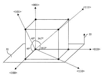
Figure 2 is an illustration showing one configuration of the ion beam, the
deposition flux, and
the substrate for a fluorite type, a pyrochlore type, or a rare earth C type
material;
Figure 3 is an illustration showing another configuration of the ion beam, the
deposition flux,
and the substrate for a fluorite type, a pyrochlore type, or a rare earth C
type material;
Figure 4 is an illustration showing one configuration between the ion beam,
the deposition
flux, and the substrate for a rock salt type material, a Re03 type material,
and perovskite type material;
Figure 5 is an illustration showing another configuration between the ion
beam, the deposition
flux, and the substrate for a rock salt type material, a Re03 type material,
and perovskite type material;
Figure 6 is an illustration showing a layer-structured material, its
crystallographic directions,
and the ion beam direction;
4
CA 02560771 2006-09-21
WO 2006/075997 PCT/US2005/011845
Figure 7 is an illustration showing a configuration between the ion beam, the
deposition flux,
and the substrate for the layer-structured material shown in Figure 6;
Figure 8 is an illustration showing a superconducting tape structure that
utilizes a layer-
structured material to obtain biaxial texture;
Figure 9 is an illustration showing an exemplary fast IBAD system for
depositing a biaxially-
textured film with an oblique incident angle deposition flux; and
Figure 10 is an illustration showing the phi-scan for a biaxially textured
film deposited using
the methods of this invention.
MODES FOR CARRYING OUT THE INVENTION
For the purposes of promoting an understanding of the invention, reference
will now be made
to some preferred embodiments of the present invention as illustrated in
FIGURES 1-10 and specific
language used to describe the same. The terminology used herein is for the
purpose of description, not
limitation. Specific structural and functional details disclosed herein are
not to be interpreted as
limiting, but merely as a basis for the claims as a representative basis for
teaching one skilled in the art
to variously employ the present invention. Any modifications or variations in
the depicted structures
and methods of making same, and such further applications of the principles of
the invention as
illustrated herein, as would normally occur to one skilled in the art, are
considered to be within the
spirit of this invention.
The present invention describes methods for deposition of high quality
biaxially-textured films
as a buffer layer for second-generation high temperature superconducting tapes
having a high critical
current density. As used herein, the critical current density refers to a
measurement of current carrying
capacity, and is abbreviated J~, measured in amperes/square centimeter (A/cm2
at OT and 77K). As is
known in the art, the critical current density in oxide films is partly
dependent upon grain-to-grain
misalignments. Higher J~ values are associated with smaller misalignment
angles. Devices utilizing
the present invention require good control over the grain alignment of the
materials therein. Frequent
high-angle boundaries impede current flow. The high-temperature
superconductors produced using the
methods described below have very high critical current densities.
As also used herein, "substrate normal" is the direction perpendicular to the
substrate surface
plane; the "deposition flux incident plane" is the plane defined by substrate
normal and the direction of
the deposition flux; and the "ion beam incident plane" is the plane defined by
substrate normal and the
direction of ion beam.
5
CA 02560771 2006-09-21
WO 2006/075997 PCT/US2005/011845
In order to create low-angle grain boundaries in a material, it is necessary
to create a biaxial
texture in the material. A biaxially-textured film, by definition, has both an
in-plane and out-of plane
crystal texture. A biaxially-textured film is defined herein as a
polycrystalline material in which both
the crystallographic in-plane and out-of plane grain-to-grain misorientation
of the surface is less than
, about 30°, such as less than about 20°, 15°,
10°, or 5°, but generally greater than about 1°. The
degree
of biaxial texture can be described by specifying the distribution of grain in-
plane and out-of plane
orientations as determined by x-ray diffraction. A full-width-half maximum (F~
of the rocking
curve of the out-of plane (OCJ) and in-plane (~~) reflection can be
determined. Therefore, the degree
of biaxial texture can be defined by specifying the range of 0D and 0~ for a
given sample. Preferably
the (0~) can be less than about 15° and (0~) can be less than about
10° for sharply textured layers.
The present invention describes methods for increasing the deposition rates of
biaxially-
textured films over the deposition rates of conventional IBAD-YSZ methods.
Typically, conventional
1BAD-YSZ deposition is performed at a rate of about O.lnm/second in order to
obtain a sharply
textured layer. The deposition rates for sharply textured layers of the
present invention are about
lnm/second or greater, preferably greater than about 2.Onm/second, and more
preferably greater than
about 3.Onm/second. The result is a rate increase of about thirty times that
of conventional methods,
which is useful for large-scale fabrication of superconducting tapes.
In conventional IBAD methods, the deposition flux is oriented normal to the
film surface. In
this invention, the deposition flux has an oblique incident angle to the film
surface, which helps achieve
faster texture evolution and results in a better film texture. Furthermore, in
this invention, the ion beam
bombardment occurs at a certain incident angle to the filin surface.
In conventional ISD methods, the deposition flux has an oblique incident angle
to the film
surface, but the <001> axis in the ISD layers is tilted off film normal,
resulting in undesired out-of
plane orientation, and a rough film surface similar to "roofing tiles." In
this invention, the deposition
rate is similar to or faster than that of conventional ISD methods, but the
<001> axis of the biaxially-
textured buffer layers of this invention does not tilt off film normal, and
more, the anisotropic growth
rate induced by ion bombardment in this invention helps to achieve a better
texture. Ion beam
bombardment in this invention also increases the atomic mobility in the film
surface and helps to obtain
a denser, smoother film.
It is well known that in ion beam assisted deposition (IBAD), when an ion beam
bombards a
growing filin at a specific angle, which usually relates to one of the film's
low index crystallographic
directions such as <1l l>, <110>, or <100>, the sharpest biaxial texture is
obtained at this incident
angle because ion beams incident along this direction have a channeling effect
and/or cause the least
damage to growing films. This incident angle is called the best ion texture
direction (BITD), and the
6
CA 02560771 2006-09-21
WO 2006/075997 PCT/US2005/011845
angle may change with different materials and/or with different deposition
parameters like the ion-to-
atom arrival ratio. In this invention, the ion beam incident angle is arranged
so that it is along the
BITD while, at the same time, the deposition flux incident plane is parallel
to the direction along which
the buffer film has a fast in-plane growth rate. Depending on the material,
the range for the deposition
flux incident angle is from about 5° to about ~0° from film
normal. Depending on the material, the
range for the ion beam incident angle is from 10-60° from film normal,
or at glancing angle (near 0°
from the substrate surface), or substantially along the substrate normal (near
0° from substrate normal).
In this invention, the materials used for the biaxially-textured filin(s) have
a fast growth rate
along one certain low index crystallographic direction, and a slow growth rate
along the other
crystallographic directions. It is well known that with, ion beam assisted
deposition, the sharpest
biaxial texture is obtained when an ion beam bombards the growing filin at a
certain specific angle. In
this invention, the ion beam incident angle is arranged so that it is along
the direction producing the
sharpest texture, while at the same time, the deposition flux incident plane
is parallel to the direction
along which the biaxially-textured film has a fast in-plane growth rate. The
overlapping of the growth
anisotropy introduced by the oblique deposition flux and the growth anisotropy
introduced by ion
bombardment yields a fast texture evolution rate.
In one exemplary embodiment, a high-rate evaporation method, such as electron
beam
2.0 evaporation (e-beam evaporation), is operable for providing the deposition
flux. In the prior art method
by X. Xiong et al. ("Rapid Deposition of Biaxially-Textured Ce02 Buffer Layers
on Polycrystalline
Nickel Alloy for Superconducting Tapes by Ion Assisted Pulsed Laser
Deposition", Physica C, 336
(2000) 70), the deposition flux was provided using excimer lasers. Excimer
lasers are very expensive
and are not cost-effective for large-scale production methods. In contrast,
the high-rate evaporation
method is cost effective and excellent for large-scale industrial
applications.
Any suitable biaxially-textured film material may be used in the present
invention, provided
that the biaxially-textured film does not adversely react with the
superconducting filin or the substrate.
In one embodiment of this invention, cubic-structured materials having a fast
growth rate direction
along the <100>, <001>, or <O10> crystal axes are used for IBAD biaxially
textured film deposition.
Such materials include, but are not limited to, fluorite type materials such
as cerium oxide (Ce02), RE
doped cerium oxide (RECe)O2, where RE is samarium, europium, erbium,
lanthanum, and yttria-
stabilized zirconia (YSZ); pyrochlore type materials such as EuzZr20~ and
Gd2Zrz0~; and rare-earth C
type materials such as ytixium oxide (Yz03). Figure 1 shows crystallographic
directions of these kinds
of materials. For these materials, and as further illustrated in Figure 2, the
film's out-of plane
orientation is along the <001> axis due to the fast growth rate along this
axis, and the BITD should be
along the <111> axis. Therefore, the ion beam 50 runs along the BITD (i.e.,
along the <1l1> axis) and
is about 55° from the substrate and film normal 55, as shown in Figure
2. Because the film's fast in-
7
CA 02560771 2006-09-21
WO 2006/075997 PCT/US2005/011845
plane growth direction is along crystal axis <100>, and the deposition flux
incident plane 53 is
arranged parallel to this direction, the angle between the deposition flux
incident plane 53 and the ion
beam incident plane 54 is about 45° or about 135°, as
illustrated in Figure 2. In this configuration of
the ion beam 50, the deposition flux 51, and the substrate 52, the deposition
flux 51 has an oblique
incident angle of about 5° to about 80°, preferably about
20° to about 55° from substrate normal 55.
Configuring the ion beam 50, the deposition flux 51, and the substrate 52 in
this manner results in the
overlapping of the anisotropic growth introduced by the ion beam and the
anisotropic growth
introduced by the oblique deposition flux, which yields fast biaxial texture
development. The ion-to-
atom arrival ratio (I/A) for these cubic structured materials is from about
0.2 to about 3, and preferably
from about 0.5 to about 1Ø The energy of the ion beam is about 150eV to
about 1500eV. The
deposition rate can be greater than about lnm/second, and preferably greater
than about 3nm/second.
The thickness of the biaxially-textured film is above about 0.2pm.
Referring now to Figure 3, there is shown an illustration showing another
configuration of the
ion beam 50, the deposition flux 51, and the substrate 52 for a fluorite type,
a pyrochlore type, or a rare
earth C type material as shown in Figure 1. Such materials include, but are
not limited to, fluorite type
materials such as cerium oxide (CeOz), RE doped cerium oxide (RECe)O2, where
RE is samarium,
europium, erbium, lanthanum, and yttria-stabilized zirconia (YSZ); pyrochlore
type materials such as
EuzZr20~ and GdZZrZO~; and rare-earth C type materials such as ytixium oxide
(Yz03). In this
embodiment, the film's out-of plane orientation is along the <001> axis due to
the fast growth rate
along <100>, <O10> or <001>, same as in the embodiment described above, but
with low ion-to-atom
arrival ratio. At a low ion-to-atom arnval ratio less than about 0.5, the BITD
or second best ion texture
direction (second BITD) is along the <110> crystal axis. Therefore, in these
embodiments, the ion
beam incident angle 50 follows the <110> crystal axis, which is about
45° from substrate normal. In
these embodiments, the deposition flux incident plane 53 is parallel to the
film's fast in-plane growth
direction <100>, or perpendicular to film's fast in-plane growth direction
under some growth
conditions, and the ion beam incident plane 54 is also parallel to the <100>
axis, so the angle between
the deposition flux incident plane 53 and the ion beam incident plane 54 is
about 0° or about 180° as
shown in Figure 3, or about 90°,. The ion beam incident angle is in the
range of about 10° to about
60°, preferably about 45°, from the substrate normal 55. The
deposition flux 51 has an incident angle in
the range of 5° to 80°, preferably about 20° to about
55° from substrate normal S5. In this
configuration, the ion-to-atom arrival ratio (I/A) needs to be less than about
0.5, preferably in the range
between about 0.05 and about 0.3; and the ion energy is about 150ev to about
1500ev, preferably, from
about SOOev to about 900ev. In this embodiment, the deposition rate can be
greater than about
lnm/second, preferably above about 3nm/second. The thickness of the biaxially-
textured film is above
about 0.2~m
8
CA 02560771 2006-09-21
WO 2006/075997 PCT/US2005/011845
In other embodiments, materials having a rock salt crystal structure such as
Mg0 (magnesium
oxide), Ba0 (barium oxide) or Ni0 (nickel oxide), or Re03 (rhenium trioxide)
type structure such as
W03 (tungsten trioxide) or, or perovskite structure such as LaAl03 (lanthium
aluminate) or SrTi03
(strontium titanate), are used for biaxially-textured film deposition. Figure
1 also illustrates the
crystallographic directions of this type of material. Compared to the fluorite
type materials discussed
above, materials with the rock salt crystal structure have larger anisotropic
sputter yield/damage along
different low index axis, which is good for texture formation by IBAD.
However, in materials with the
rock salt crystal structure, it is difficult to obtain <001> out-of plane
orientation under dynamic growth
condition because the growth rates along the <1l1> and <110> axes are higher
than along the <001>
axis. Generally, the only way to get <001> out-of plane orientation in these
materials is to apply
thermodynamic conditions (i.e., high temperatures). However, there is one
special case where <001>
out-of plane orientation can be achieved at low temperature in these materials
- during the initial
nucleation stage. During the initial fllin growth of ionic crystals such as
Mg0 or NiO, charge effect
plays a dominating role during nucleation stage. The charge-balanced <001>
plane of the Mg0 or Ni0
has the lowest energy to nucleate so the resulting film will have <001> out-of
plane orientation. As the
film grows thicker, the importance of charge effect is reduced, and the film
out-of plane orientation
changes to the <111> or <110> axis, depending upon the deposition conditions.
Therefore, the film
growth needs to be stopped after a certain thickness in order to prevent this
change in the out-of plane
orientation. This mechanism is used in IBAD Mg0 process. In this invention,
because the fast growth
direction for such materials is supposed to be along the <1l1> axis, and the
BITD is supposed to be
along the <100>, <001>, <O10> axis, in order to obtain <001> out-of plane
orientation, as shown in
Figure 4, the ion beam 50 bombards the film 52 along the substrate normal SS
with ion energy of about
300ev to about 1500ev to force the film to have <001> out of plane
orientation, while at same time, the
deposition flux 51 has an oblique incident angle of about 20° to about
80° from substrate normal 55,
preferably about 45 to about 65°, along the <1l1> direction. Because
the ion beam 50 in this invention
bombards the filin along the substrate normal 55, the ion bombardment does not
introduce in-plane
anisotropic growth. The anisotropic growth here is solely introduced by the
oblique incident angle of
the deposition flux 51, as in the ISD method. However, unlike the ISD method,
in this invention, the
<001> axis is not tilted from substrate normal 55, but rather, it is
substantially parallel to substrate
normal 55. In this embodiment, the deposition rate can be greater than about
lnm/second, preferably
above about 3nm/second.
In other embodiments of rock salt type materials, or Re03 type material, or
perovskite type
material, in order to introduce in-plane anisotropic growth by the oblique ion
beam bombardment, as
shown in Figure 5, the ion beam 50 bombards the film 52 at a glancing angle (a
few degrees from the
film surface, typically around 5°), and the angle between the ion beam
incident plane 54 and the
deposition flux incident plane 53 is about 45° or about 135°. In
this case, the ion beam 50 is roughly
along the <O10> direction, the <lll> axis is within the deposition flux
incident plane 53, and the
9
CA 02560771 2006-09-21
WO 2006/075997 PCT/US2005/011845
deposition flux 51 has an oblique incident angle of about 5° to about
80° from substrate normal 55,
preferably about 45 to about 65°, along the <1l1> direction. The ion
energy is about 300ev to about
1500ev, preferably in the range between about 700eV and about 900eV. In the
embodiment, the
biaxially texture of the deposited film can be due to growth selection
mechanism like in conventional
IBAD YSZ or ISD MgO, or/and due to biaxial nucleation mechanism like in IBAD
MgO. In this
embodiment, unlike IBAD MgO, the film's out-of plaue orientation will not
changes to the <1 l 1> or
<110> axis when film grows thicker than about lOnm, and sharper biaxial
texture and higher yield of
sharp texture is obtained compared to IBAD Mg0 process. Another advantage of
this embodiment is
that it does not put high demand on the substrate surface roughness, and also
does not need additional
homo-epitaxiallayers.
In another embodiment of rock salt, Re03 or perovskite materials with fastest
growth rate
direction along crystal axis <1l1> and a best ion texture direction (BITD) or
a second best ion texture
direction along <110> crystal direction., the biaxially textured film is
produced using an ion beam
incident angle, which is about 45° from film normal, and using a
deposition flux incident angle in the
range between about 45° to about 65° from Olin normal. In this
case, the ion-to-atom arrival ratio (I/A)
is from about 0.2 to about 3, preferably between about 0.5 and about 1.
In another embodiment, non-cubic, layer-structured materials having strong
anisotropic
growth rates are used for IBAD biaxially-textured film deposition with an
oblique incident deposition
flux to achieve a sharp texture. Such materials include, but are not limited
to, deformed perovskite
structured materials such as REBaZCu307_s (where RE is one of yttrium,
gadolinium, terbium,
dysprosium, lanthanum, neodymium, samarium, europium, holmium, erbium,
thulium, and/or
ytterbium) and rutile type material such as Ti02, Sn02, WOZ, RuOz, MnOz, NbOz,
VO2, IrOz. Figure 6
is an illustration showing a layer-structured material, its crystallographic
directions, and the ion beam
direction. In these embodiments, the growth rate along the a-axis (i.e., the
<100> crystal axis) and the
b-axis (i.e., the <O10> crystal axis) can be several times higher than the
growth rate along the c-axis
(i.e., the <001> crystal axis). In dynamically-dominating growth, the out-of
plane orientation of the
resulting film will be along the a-axis because that is the fast growth
direction. The slow growth c-axis,
and the other fast growth b-axis, lies in film plane 52. The strong in-plane
growth anisotropy between
the c-axis and the b-axis will greatly benefit the biaxial texture evolution
with the oblique deposition
flux. Due to characteristics of the layered structure, the BITD in such
materials is parallel to the layer
plane (i.e., the a-b plane), as shown in Figure 6. As shown in Figure 7, in
these embodiments, the ion
beam 50 bombards the fllin 52 at an incident angle of about 45° from
substrate normal 55, and the
angle between the ion beam incident plane 54 and the deposition flux incident
plane 53 is about 0° (or
about 180°), or about 90° (or about 270°) in certain
growth conditions. The ion beam incident angle 51
is in the range between about 35° and about 60°, preferably
45°, from the substrate normal 55, or
substantially along substrate normal (about 0°), or at a glancing angle
from substrate surface depending
on different material used. The deposition flux incident angle is in the range
between about 10° to
CA 02560771 2006-09-21
WO 2006/075997 PCT/US2005/011845
about 65° from substrate normal. Configuring the ion beam 50, the
deposition flux 51, and the substrate
52 in this manner results in the overlapping of the anisotropic growth
introduced by the ion beam and
the anisotropic growth introduced by the oblique deposition flux to yield fast
biaxial texture
development. In this embodiment, the deposition rate can be greater than about
lnm/second,
preferably above about 3nm/second.
The layer-structured material is often a mufti-component material. Therefore,
in order to get
the right composition and stoichiometry during this mufti-component
deposition, the substrate
temperature some times is increased above a value at which the layer-
structured composition is stable,
preferably the substrate temperature (and corresponding deposition
temperature) is about 200°C to
about 600°C. The deposition temperature for obtaining the right
composition and stoichiometry of the
mufti-component material can be determined from phase diagrams. Active oxygen,
such as atomic
oxygen, ozone, oxygen ions, NzO, etc., may be used to reduce the required
deposition temperature.
In all embodiments of the invention, especially in the embodiments of rock
salt type material,
RE03 type material, perovskite type material and non-cubic, layer-structured
material, in order to
prevent epitaxial growth from substrate and oxidation of substrate, an
intermediate layer is deposited
on said substrate before the deposition of said biaxially textured film, if
necessary. The function of
intermediate layer is achieved by using materials with large lattice mis-match
between said
intermediate buffer and the said biaxially-textured film, and/or by
controlling the grain size of said
intermediate buffer layer as small as possible, preferably in manometer scale.
The lattice mis-match is
larger than about 10%, preferably larger than about 20%. In order to obtain
small grain size the
material of said intermediate layer is usually chosen from material with large
free energy of formation.
Although prior art methods utilize an amorphous layer before deposition for
biaxially textured filin like
IBAD MgO, the intermediate layer utilized herein is not necessary an amorphous
layer so that wider
range of material with various other properties can be chosen from, and put
lower demand on
deposition conditions.
Referring now to Figure 8, there is an illustration showing a superconducting
metal substrate
such as a tape structure 20 that utilizes a non-cubic layer-structured
material to obtain biaxial texture.
To prevent epitaxial growth on the substrate 10, and to prevent oxidation of
the metal substrate at high
temperatures, an intermediate layer 12 (having manometer grain size and having
large lattice mis-match
with biaxially textured film) may optionally be deposited on the metal
substrate 10 before ion beam
assisted deposition of the biaxially-textured film 14. The intermediate layer
12 may comprise rare
earth C type materials such as Yz03, Eu203, or Pr203; or oxides such as
yttrium stabilized zirconium
oxide (YSZ); or nitrides such as silicon nitride (Si3N4). The thickness of
this intermediate layer 12 can
be about lOnm to about 300nm. An epitaxial buffer layer 16 of cubic structured
material, having a
good lattice match with YBCO, may optionally be deposited on the top of the
biaxially-textured filin(s)
14, if desired, prior to deposition of the superconducting layer YBCO 18. Some
exemplary cubic
11
CA 02560771 2006-09-21
WO 2006/075997 PCT/US2005/011845
structured materials 16 comprise Ce02, SrTi03, LaMn03, LaZr03, and/or GaZr03.
High temperature
superconducting layer 18 can then be coated on this epitaxial buffer layer 16.
Although prior art
methods utilize an amorphous layer before deposition for biaxially textured
film like 1BAD MgO, the
intermediate layer utilized herein does not put high demand on the substrate
surface roughness, and
also does not need additional homo-epitaxial layers.
One exemplary process for creating a biaxially-textured film of a fluorite
type material as
mentioned above is as follows:
(1.) A metal tape, such as a Ni-based alloy, is electropolished or chemical-
mechanically
polished to an average roughness of less than about l Onm.
(2.) Next, a biaxially-textured film of fluorite type material is deposited at
a high
deposition rate (greater than about 1 nm/s, preferably greater than about 3
nm/s) on the metal tape by a
high rate evaporation method, such as e-beam evaporation, with simultaneous
ion beam bombardment
at an oblique angle of about 45°, from tape normal. The deposition flux
is arranged so that it has an
oblique incident angle of 25°, from tape normal. The deposition flux
incident plane is parallel to the
ion beam incident plane. The ion-to-atom arrival ratio is controlled to be
around 0.1. The thickness of
the biaxially-textured fllin is about 1500- 2000nm.
(3.) Thereafter, a thin epitaxial buffer film (less than about 100nm) is
deposited onto the
biaxially-textured film. Depending on the material used for the biaxially-
textured film, the thin,
epitaxial film may be omitted, if desired. The material of the epitaxial
buffer layer may comprise, but
is not limited to, cerium oxide (CeOz) and/or strontium titanate (SrTi03).
(4.) Finally, a YBCO layer with a thickness greater than about 1000nm is grown
on the
buffer layer structure. Therefore the buffer layer structure may consist of
the required biaxially-textured
film and the optional epitaxial film.
The high temperature superconductors of this invention generally comprise at
least: a
substrate, a biaxially-textured film by the methods described in this
invention, in claim 1, claim 41,
claim 53, claim 66, and a superconducting layer. In various embodiments of the
present invention, the
substrate may include, but is not limited to, any polycrystalline metal or
metal alloy such as nickel
alloy and the like. Nickel alloy may be preferred due to its high strength and
temperature-resistant
properties. During the deposition of the superconducting layer, it is
necessary to achieve temperatures
of about 800°C. Various alloys, such as Hastelloy (Ni-Cr-Mo alloy) and
Inconel~ (Ni-Cr-V alloy),
are resistant to oxygen and are suitable for use in the present invention. The
metal substrate, on which
the biaxially-textured film is deposited, should preferably provide
flexibility to the whole structure so
12
CA 02560771 2006-09-21
WO 2006/075997 PCT/US2005/011845
that the structure may be shaped and wound in the form of a tape, cable or
coil for all electric power
applications. The metal substrate should be as thin, preferably less than
about O.lSmm, and flexible as
possible.
As previously discussed, the biaxially-textured film may comprise any suitable
material that
does not adversely react with the superconducting layer or the substrate. The
materials used for these
biaxially-textured films) have a fast growth rate along certain low index
crystallographic directions,
and a slow growth rate along the other crystallographic directions. An ion
beam can be used to
bombard the growing film simultaneously under various configuration of ion
beam, deposition flux and
substrate normal; this configuration is depended on the materials and
deposition conditions used. The
materials used for these biaxially textured films may comprise, but are not
limited to, fluorite type
materials such as cerium oxide (CeOz) and ytiria-stabilized zirconia (YSZ);
pyrochlore type materials
such as EuZZr20~ and Gd2Zr20~; and rare-earth C type materials such as ytixium
oxide (YZO3), rock salt
type material, Re03 type material, perovskite type material, non-cubic
material with strong anisotropic
growth rate. The biaxially-textured films may be applied by any of a variety
of conventional methods,
using at least one of evaporation method including resistive heating
evaporation, co-evaporation,
electron beam evaporation, magnetron sputtering, pulsed laser ablation, ion
beam sputtering, molecular
beam epitaxy
A superconducting layer may be subsequently deposited upon the buffer layer
structure. The
superconducting layer may be applied by any of a variety of conventional
methods including, but not
limited to, evaporation including co-evaporation, electron beam evaporation,
sputtering including
magnetron sputtering, ion beam sputtering and ion assisted sputtering,
chemical vapor deposition,
metal organic chemical vapor deposition, plasma enhanced chemical vapor
deposition, molecular beam
epitaxy, a sol-gel process, a solution process, andlor liquid phase epitaxy.
Suitable examples of superconductor materials include, but are not limited to,
oxide
superconductor materials, such as yttrium barium copper oxides (YBa2Cu30~_s),
rare-earth barium
copper oxides, and mixtures of the two materials. In the case of rare-earth
barium copper oxides, the
yttrium of YBCO may be partially or completely replaced by rare-earth metals
from the periodic table
such as, but not limited to, gadolinium, terbium, dysprosium, lanthanum,
neodymium, samarium,
europium, holinium, erbium, thulium and ytterbium. The superconducting
material is preferably
YBCO, although other minor variations of this basic superconducting material
may be used. The
superconducting layer may have a general thickness in the range of about l.O~m
to about 20.Opm,
more preferably in the range of about l.O~m to about lO.Opm. The thickness of
the superconducting
layer may vary for selected applications.
13
CA 02560771 2006-09-21
WO 2006/075997 PCT/US2005/011845
Figure 9 is an example of a Fast IBAD System with Oblique Deposition Flux
(FIBAD/ODF).
A 6 x 66 cm RF ion gun 38 was installed in a vacuum system with a base
pressure better than 5 x 10⁻⁶
Torr, which bombards the tape 42 at an incident angle of about 45°
between the ion beam 44 and tape
normal 43. Argon was used in the ion gun and neutralizer. Oxygen, preferably
active oxygen, was
provided near the tape 42. The working pressure was about 1.4 x 10~ Torr.
Normal ion energy was
about 760eV. The ion current density at the tape position was about
0.52mA/cmz. The deposition zone,
defined by an aperture, was about 8.8cm by about 60cm. Three rod-feed
electronic beam evaporating
sources 40, lined up along a long direction of the deposition zone, provided a
uniform CeOz deposition
rate about 4.lnm/s at the tape deposition zone. The ion to atom ratio is about
0.13. The tape holder 36
was tilted by about 45°, so the e-beam deposition flux had
approximately a 45° oblique angle to the
tape normal 43. The tape 42 was electropolished or chemical-mechanically
polished to an average
roughness of less than about l Onm. The tape 42 continuously moved in a
direction normal to the paper
of the drawing, perpendicular to both the ion beam 44 and the deposition flux.
The tape 42 had good
contact with the tape holder 36, and could either be water-cooled or heated by
the tape holder. The
deposition flux, ion beam and tape normal were all in the same plane. The
biaxially-textured film was
deposited to a thickness of about 1,800nm while moving through the deposition
zone, either in a single
pass or in multiple passes. The resulting film had its <002> crystal axis
along tape normal, and its
<020> crystal axis in the ion beam incident plane. The FWHINl of phi-scan of
biaxially texture film
was about 11 °, as shown in Figure 10, providing a good template for
the epitaxial growth of a
superconducting layer, a layer resulting in a critical current density greater
than about 1 MA/cmz.
The superconductor article may be employed in a power cable. In one
embodiment, the power
cable may comprise a plurality of superconductive tapes, wherein each tape
comprises a substrate; a
biaxially-textured film produced by the methods described in present
invention; and a superconducting
layer. In a further embodiment, the power cable may comprise a conduit for the
passage of a coolant
fluid, and the superconductive tapes may be wrapped around the conduit.
The superconductor article may be employed in a power transformer. In one
embodiment, the
power transformer may comprise a plurality of windings, wherein each winding
comprises a wound
coil of superconductive tape, wherein each tape comprises a substrate; a
biaxially-textured film
produced by the methods described in this invention; and a superconducting
layer.
The superconductor article may be employed in a power generator. In one
embodiment, the
power generator may comprise a shaft coupled to a rotor comprising
electromagnets comprising at least
one rotor coil, and a stator comprising a conductive winding surrounding the
rotor, wherein at least one
of the winding and the at least one rotor coil comprises a superconductive
tape. As above, each
superconductive tape comprises a substrate; a biaxially-textured film produced
by the methods
described in this invention; and a superconducting layer.
14
CA 02560771 2006-09-21
WO 2006/075997 PCT/US2005/011845
The superconductor article may be used in a power grid. In one embodiment, the
power grid
may comprise a power generation station comprising a power generator, a
transmission substation
comprising a plurality of power transformers, at least one power transmission
cable, a power
substation, and at least one power distribution cable. The plurality of
transformers are operable for
receiving power from the power generation station and stepping-up voltage for
transmission. The
power transmission cables are operable for transmitting power from the
transmission substation. The
power substation is operable for receiving power from the power transmission
cables, and comprises a
plurality of power transformers for stepping-down voltage for distribution.
The at least one power
distribution cable is operable for distributing power to an end user. The
power transmission cables,
power distribution cables, transformers of the power substation, transformers
of the transmission
substation, and the power generator may comprise a plurality of
superconductive tapes. Each
superconductive tape comprises a substrate; a in biaxially-textured film
produced by the methods
described this invention; and a superconducting layer.
The foregoing is a description of some preferred embodiments of this
invention, which are
given here by way of example only. Although the biaxially-textured film
deposition methods of the
present invention have been described with reference to preferred embodiments
and examples thereof,
other embodiments and examples may perform similar functions and/or achieve
similar results. All
such equivalent embodiments and examples are within the spirit and scope of
the present invention and
are intended to be covered by the following claims.