Note: Descriptions are shown in the official language in which they were submitted.
CA 02560820 2006-09-22
WO 2005/096221 PCT/US2004/042627
LOW COST METHOD OF PRODUCING RADIO FREQUENCY IDENTIFICATION
TAGS WITH STRAPS WITHOUT ANTENNA PATTERNING
BACKGROUND OF THE INVENTION
1. Field of the Invention
[0001] This invention relates to the field of Radio Frequency Identification
(RFID)
tags and labels, and in particular to a method of producing such tags and
devices
without antenna patterning.
2. Description of the Related Art
[0002] Radio frequency identification (RFID) tags and labels (collectively
referred
to herein as "devices") are widely used to associate an object with an
identification
code. RFID devices generally have a combination of antennas and analog and/or
digital electronics, which may include for example communications electronics,
data
memory, and control logic. For example, RFID tags are used in conjunction with
security-locks in cars, for access control to buildings, and for tracking
inventory and
parcels. Some examples of RFID tags and labels appear in U.S. Patent Nos.
6,107,920, 6,206,292, and 6,262,292, all of which are hereby incorporated by
reference in their entireties.
[0003] As noted above, RFID devices are generally categorized as labels or
tags.
RFID labels are RFID devices that are adhesively or otherwise attached
directly to
objects. RFID tags, in contrast, are secured to objects by other means, for
example
by use of a plastic fastener, string or other fastening means.
[0004] Typically, RFID devices are produced by patterning, etching or printing
a
conductor on a dielectric layer and coupling the conductor to a chip. These
structures furthermore should be able to flex when supported at one or more
ends. It
is important therefore to avoid materials and constructions that add undue
thickness
or stiffness to the RFID tag. Considering the requirements of thinness and
flexibility,
conductors such as wirebonds and metal lead frame are unsuitable, as are
related
materials such as epoxy encapsulation, and thinner conductors are desirable
(such
as printed conductive inks).
[0005] RFID devices on the other hand should have adequate electrical
connections, mechanical support, and appropriate positioning of the components
1
CA 02560820 2006-09-22
WO 2005/096221 PCT/US2004/042627
(chips, chip connectors, antennas). Structures for these purposes can add
complexity, thickness and inflexibility to the RFID device. For example,
layers in
addition to the dielectric substrate/connectors are sometimes added to
position the
radio frequency circuit and antenna in three dimensions to provide electrical
bonds
between the various conductors. The antenna and connecting conductors often
require more than one plane of electrical wiring, i.e. the designs may use
cross-overs
and stacking of components.
[0006] One type of structure that may carry chips and chip connectors for
incorporation in RFID devices is a "strap" or "interposer", as disclosed for
example in
U.S. Patent No. 6,606,247 or in European Patent Publication 1 039 543, both of
which are incorporated by reference herein in their entireties.
[0007] Another consideration is efficiency of manufacture of RFID devices.
When
using thin deposited or etched conductors, the precision and definition of the
printed
elements of lines and spaces may be important to the performance of the tabs
and
the overall RFID device. Conventional patterning, etching and printing methods
may
not provide adequate resolution, line/space separation or other qualities
necessary
to deliver engineered performance. In addition, methods of manufacturing RFID
devices that include combining a web of RFID chips or straps with a web of
formed
or printed RFID antennas are complicated by the need to account for any
differences
in the pitch of each web, or spacing between adjacent element on each web, so
that
the RFID chips or straps and antennas are aligned. Further details regarding
indexing of RFID strap webs may be found in co-owned U.S. Patent Application
2003/0136503 A1, which is herein incorporated by reference in its entirety. It
is also
desirable from a manufacturing perspective to reduce complexity and
manufacturing
steps in RFID device designs, and to make efficient use of component materials
(reduce waste).
[0008] Moreover, while RFID tags and labels are inexpensive, and costs of RFID
devices have been going down, the size and cost of such devices may make them
impractical for use with small or inexpensive items. Therefore it is important
to
achieve the properties described above, especially for thin flexible RFID tags
and
labels, through cost-effective manufacture of such devices.
[0009] From the foregoing it will be seen there is room for improvement of
RFID
devices and manufacturing processes relating thereto.
2
CA 02560820 2006-09-22
WO 2005/096221 PCT/US2004/042627
SUMMARY OF THE INVENTION
(0010] According to an aspect of the invention, a web includes a conductive
layer
atop an insulating layer, the conductive layer having one or more apertures
therein to
create suitable coupling points. Alternatively, the web may not include an
insulating
layer. The web includes a plurality of radio frequency identification (RFID)
devices,
with each of the devices including a pair of antennas that are areas or
sections of the
conductive material, and an RFID chip or strap across one of the one or more
apertures or lines of apertures, electrically coupled to the antennas. The
antennas of
various of the RFID devices may be tessellated with one another, with antennas
of
different devices having complementary shapes wherein the boundary of one of
the
antennas is also the boundary of an adjacent antenna. According to various
specific
embodiments, the webs may have rectangular shapes, curved shapes such as
sinusoidal shapes, generally triangular shapes, or other shapes.
[0011] According to another aspect of the invention, a web includes a
conductive
layer atop an insulating layer, the conductive layer having an aperture in the
longitudinal or length direction of the web. The web includes a plurality of
radio
frequency identification (RFID) devices, with each of the devices including a
pair of
antennas that are areas or sections of the conductive material, and an RFID
chip or
strap across the aperture.
[0012] According to yet another aspect of the invention, a web includes a
conductive layer atop an insulating layer, the conductive layer having a
plurality of
apertures in a transverse or width direction of the web. The web includes a
plurality
of radio frequency identification (RFID) devices, with each of the devices
including a
pair of antennas that are areas or sections of the conductive material, and an
RFID
chip or strap across one of the apertures, between the areas or sections.
[0013] According to still another aspect of the invention, a web includes a
conductive layer atop an insulating layer, the web including one or more folds
or
creases therein to produce one or more corresponding apertures in the
conductive
layer. RFID chips or straps may be placed across an aperture to form a
plurality of
RFID devices, with each chip or strap electrically coupled to sections of the
conductive layer that serve as antenna elements. The one or more apertures may
3
CA 02560820 2006-09-22
WO 2005/096221 PCT/US2004/042627
be in a longitudinal direction (in the length or long direction of the web) or
may be in
a transverse direction (in the width or short direction of the web).
[0014] According to a further aspect of the invention, a method of making RFID
devices may include placing RFID chips or straps across one of one or more
apertures in a conductive layer of a web of material, thereby electrically
coupling the
RFID chips or straps to sections of the conductive layer on opposite sides of
the
aperture. The sections of the conductive layer serve as antennas of the RFID
devices, when the RFID devices are separated from one another, as by cutting.
According to one embodiment of the invention, the method may also include
forming
the one or more apertures. According to one specific embodiment of the
invention,
the forming may include folding or creasing various portions of the web, and
removing a part of the folded portion, as by cutting, to create
discontinuities in the
conductive portions, to thereby form the one or more apertures.
[0015] According to an aspect of the present invention, an RFID device is
produced
by a low cost method of manufacture utilizing conventional roll-to-roll
manufacturing
technology. Specifically, the present invention provides a method of making an
RFID device from a web material including a conductive layer having one or
more
apertures and a continuous dielectric layer. The method comprises the steps of
providing a web material including a continuous conductive layer and a
continuous
dielectric layer, forming at least one crease portion in the web material, the
crease
portion including a central portion of overlapped web material between
adjacent
portions of single ply web material, forming an aperture in the conductive
layer by
removing at least part of the central portion of the at least one crease
portion; and
applying at least one strap across the crease portion. The aperture aids in
creating
suitable coupling points for the strap to the antenna.
[0016] According to another aspect of the present invention, a method of
making an
RFID device includes the steps of: providing a web material including a
continuous
conductive layer and a continuous dielectric layer; forming at least one
aperture in
the conductive layer; and applying at least one strap across the at least one
aperture.
[0017] According to yet another aspect of the present invention, a method of
making an RFID device includes the steps of: providing a web material
including a
continuous conductive layer and a continuous dielectric layer; forming at
least one
4
CA 02560820 2006-09-22
WO 2005/096221 PCT/US2004/042627
crease portion in the web material, the crease portion including a central
portion of
overlapped web material between adjacent portions of single ply web material;
forming an aperture in the conductive layer by removing at least part of the
central
portion of the at least one crease portion; and applying at least one strap
across the
crease portion.
[0018] According to still another aspect of the present invention a web of
RFID
devices is provided comprising: a web material having a conductive layer and a
dielectric layer; at least one aperture in the conductive layer forming at
least two
separate conductor portions; at least one RFID device, including a strap
attached
across the aperture, and coupled to a conductor portion on each side of the
aperture.
[0019] According to still another aspect of the present invention a web of
RFID
devices is provided comprising: a conductive web material, at least one
aperture in
the conductive web material forming at least two separate conductor portions,
and at
least one RFID device. The RFID device includes a strap attached across the
aperture and coupled to a conductor portion on each side of the aperture.
[0020] According to yet another aspect of the invention a method of making an
RFID device is provided comprising the steps of: providing a web of conductive
material, forming at least one aperture in the web of conductive material, and
applying at least one strap across the at least one aperture.
[0021] According to yet another aspect of the invention a method of testing a
web
of
RFID devices is provided comprising the steps of: providing a web of RFID
devices,
cutting a slit in the web on opposite sides of an RFID device, wherein the
slits
partially separate a central portion of the RFID device from the web of RFID
devices,
deflecting the central portion of the RFID device from the plane of the web,
and
testing the RFID device.
[0022] According to still another aspect of the invention, a method of
programming a web of RFID devices is provided comprising the steps of:
providing a
web of RFID devices, cutting a slit in the web on opposite sides of an RFID
device,
wherein the slits partially separate a central portion of the RFID device from
the web
of RFID devices, deflecting the central portion of the RFID device from the
plane of
the web, and programming the RFID device.
CA 02560820 2006-09-22
WO 2005/096221 PCT/US2004/042627
[0023] According to another aspect of the invention, in a preferred embodiment
the
dielectric layer and conductive layers together comprise a thin, flexible
sheet
material. In this embodiment the layers are sufficiently flexible to be folded
or formed
in a roll.
[0024] According to a further aspect of the invention, a web of conductive
material
has one or more apertures therein, thereby creating suitable connect points on
the
conductive material, on opposite sides of at least one of the apertures, for
coupling
of an RFID strap or interposes to the conductive layer. The coupling of the
RFID
strap or interposes to the conductive material may be either in a direct
electrically
conductive electrical connection, or alternatively may involve capacitive
coupling.
The one or more apertures may electrically isolate the conductive material
coupled
to opposite sides of the RFID strap or interposes. Alternatively, the one or
more
apertures may still leave one or more continuous bridges of conductive
material
between the conductive material coupled to opposite side of the RFID strap or
interposes, while still creating suitable coupling points on the conductive
material for
coupling of the RFID strap or interposes. The apertures may have any of a
variety of
suitable shapes. In addition, the apertures may be formed in any of a variety
of
suitable ways, such as (for example) by folding and cutting, laser ablation,
etching,
or selective deposition of conductive material.
[0025] To the accomplishment of the foregoing and related ends, the invention
comprises the features hereinafter fully described and particularly pointed
out in the
claims. The following description and the annexed drawings set forth in detail
certain
illustrative embodiments of the invention. These embodiments are indicative,
however, of but a few of the various ways in which the principles of the
invention
may be employed. Other objects, advantages and novel features of the invention
will become apparent from the following detailed description of the invention
when
considered in conjunction with the drawings.
BRIEF DESCRIPTION OF THE DRAWINGS
[0026] In the annexed drawings, which are not necessarily according to scale,
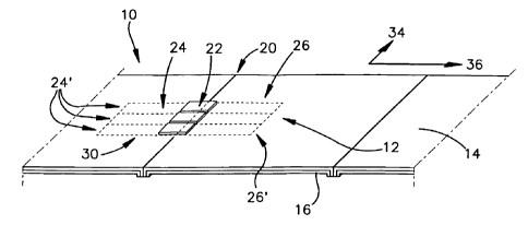
[0027] FIG. 1 is an oblique view of a web of RFID devices of the present
invention;
[0028] FIG. 2 is an oblique view of a web of RFID devices according to another
embodiment of the present invention;
6
CA 02560820 2006-09-22
WO 2005/096221 PCT/US2004/042627
[0029] FIG. 3 is an oblique view of a web of RFID devices in a partially
tessellated
configuration;
[0030] Fig. 4 is an oblique view of a web of RFID devices in a fully
tessellated
configuration;
[0031] FIG. 5 is an oblique view of a web of RFID devices in another fully
tessellated configuration;
[0032] FIG. 6 is an oblique view of a web of RFID devices wherein the
conductor
apertures extend in the transverse direction of the web material;
[0033] FIG. 7 is a top view of a strip of end-to-end aligned RFID devices;
[0034] FIG. 8 is an oblique view of a sheet of web material;
[0035] FIG. 9 is an oblique view of a partially transversely creased web
material;
[0036] FIG. 10 is an oblique view of a fully creased web material;
[0037] FIG. 11 is an oblique view of a fully creased web material with straps;
[0038] FIG. 12 is an oblique view of a web material having an aperture in the
conductive layer and a strap coupled to the conductive material across the
aperture;
[0039] FIG. 13 is an oblique view of a single RFID device according to the
present
invention;
[0040] FIG. 14 is an oblique view of a strip of end-to end aligned RFID
devices
according to the present invention;
[0041] FIG. 15 shows a strip of end-to-end aligned RFID devices being cut into
individual RFID devices;
[0042] FIG. 16 shows a system for making a web of RFID devices as in FIG. 6;
[0043] FIG. 17 is an oblique view of a web of RFID devices according to
another
embodiment of the present invention;
[0044] FIG. 18 is a plan view of a web of RFID devices, as shown in FIG. 17,
being
cut into individual RFID devices;
[0045] FIG. 19 is an oblique view of a sheet of web of material;
[0046] FIG. 20 is an oblique view of a partially longitudinally creased web
material;
[0047] FIG. 21 is an oblique view of a fully creased web material;
[0048] FIG. 22 is an oblique view of a fully creased web material with straps;
[0049] FIG. 23 is an oblique view of a web material wherein the crease is
being cut
to form an aperture in the conductive layer;
7
CA 02560820 2006-09-22
WO 2005/096221 PCT/US2004/042627
[0050] FIG. 24 is an oblique view of a single RFID device according to the
present
invention;
[0051] FIG. 25A shows a system for making a web of RFID devices as in FIG. 17;
[0052] FIG. 25B shows an oblique view of straps being applied;
[0053] FIG. 26A is an oblique view of a strip of straps being laminated to a
web
material across an aperture in the conductive layer of the web material;
[0054] FIG. 26B is an oblique view of a web of RFID devices according to
another
embodiment of the present invention;
[0055] FIG. 27 is a top view of a web of RFID devices;
[0056] FIG. 28 is a top view of a web of RFID devices;
[0057] FIG. 29 is view of a web of RFID devices with slits on each side of an
RFID
device;
[0058] FIG. 30 is an oblique view of an RFID testing/programming assembly; and
[0059] FIG. 31 is an oblique view of yet another web of RFID devices in
accordance with the present invention.
DETAILED DESCRIPTION
[0060] A web of radio frequency identification (RFID) devices includes a
conductive
layer atop an insulating layer, the conductive layer having one or more
apertures
therein. RFID chips or straps are electrically coupled to portions of the
conductive
layer on either side of one or more apertures, for use as antennas when the
RFID
devices are separated from one another, as by cutting.
[0061] The apertures may be formed by folding or creasing portions of the web,
and removing parts of the folded or creased portion as set forth herein. The
apertures may also be formed by a selective masking and evaporation process,
or
by any other suitable means. There may be a single aperture in a longitudinal
direction of the web, or multiple apertures in a longitudinal or transverse
direction of
the web. The apertures may fully separate the conductive material on either
side, or
alternatively may only partially separate the conductive material, leaving one
or more
conductive bridges linking the conductive material on both sides of the
apertures.
The shapes of the antennas of various of the RFID devices may be tessellated,
nesting within one another or having the same boundary, thereby improving
efficiency by using substantially all of the conductive material. The web may
be cut
8
CA 02560820 2006-09-22
WO 2005/096221 PCT/US2004/042627
into strips each containing a line of RFID devices, which may then be placed
on or in
individual objects. The web also may be combined with one or more additional
layers or structures, such as protective layers or printable layers, in
forming RFID
devices.
[0062] Referring initially to FIG. 1, a web 10 includes a plurality of radio
frequency
identification (RFID) devices 12. The web 10 includes an electrically-
conductive
layer or material 14 atop an electrically-insulating layer or substrate 16. As
used
herein, "conductive" means electrically conductive, and "insulating" and "non-
conductive" mean electrically non-conductive. In the embodiment shown in FIG.
1,
the conductive layer 14 has a plurality of apertures 20 therein. RFID straps,
interposers, or chips 22 are each placed across one of the apertures 20, with
the
RFID straps (interposers) 22 electrically coupled to portions 24 and 26 of the
conductive layer 14 on either side of the aperture 20. The RFID straps 22 may
be
attached to portions 24 and 26 in any number of different ways, such as
soldering, or
bonding with a conductive or nonconductive adhesive. When the RFID devices 12
are separated from one another, such as by one or more cutting operations, the
portions 24 and 26 serve as antennas for the RFID devices 12.
[0063] The RFID straps or interposers 22 may be any of a variety of
combinations
of wireless communication devices (RFID chips) with conductive leads coupled
thereto to facilitate electrical connection. The term "strap," as used herein,
may refer
to an integrated circuit (IC) chip, electrical connectors to the chip, and
strap leads
coupled to the electrical connectors. A strap also may include a strap
substrate,
which may support other elements of the strap, and may provide other
characteristics such as electrical insulation. The strap may be elongate, as
the strap
leads extend from the IC chip. The strap may be flexible, rigid, or semi-
rigid. It will
be appreciated that a variety of strap configurations are available for
coupling to the
antennas 34 and 36. Examples include an RFID strap available from Alien
Technologies, and the strap marketed under the name I-CONNECT, available from
Philips Electronics. The term "strap" broadly includes chip carriers such as
interposers. Chips available from Alien Technologies may be attached either
conductively, in a flip-chip die, or conductively or reactively for a strap
form of the
chip. Suitable RFID chips include the Philips HSL chip, available from Philips
Electronics, and the EM Marin EM4222, available from EM Microelectronic-Marin
9
CA 02560820 2006-09-22
WO 2005/096221 PCT/US2004/042627
SA, as well as RFID chips available from Matrics Inc. of Columbia, Maryland
USA.
RFID tags with adaptive elements may also be used, such as the RFID tags
described in U.S. Provisional Application No. 60/517,156, filed November 4,
2003,
which is hereby incorporated by reference.
[0064] As noted above, the RFID straps 22 may be coupled to the antenna
portions
24 and 26 by any of a variety of suitable methods, such as, for example, by
use of a
conductive or non-conductive adhesive, by use of welding and/or soldering, or
by
electroplating. Thus the straps 22 may be conductive coupled to the antenna
portions 24 and 26 directly, through continuous contact of electrically
conductive
material. Alternatively, the electrically coupling between the straps 22 and
the
antenna portions 24 and 26 may be capacitive or inductive, across a layer of
non-
conductive material. For example, a non-conductive adhesive or glue may be
used
to adhere the straps 22 to the antenna portions 24 and 26, with capacitive or
inductive electrically coupling occurring across the layer of non-conductive
material.
[0065] The straps or interposers 22 are coupled to the antenna portions 24 and
26
at suitable attach or connect points 24' and 26' on the antenna portions 24
and 26.
The attach or connect points 24' and 26' on the antenna portions 24 and 26 may
be
selected so as to achieve desired operative coupling between the straps or
J
interposers 22, and the antenna portions 24 and 26. For instance, the attach
or
connect points 24' and 26' may be selected such that the impedance across the
attach or connect points 24' and 26' is the complex conjugate of the impedance
of
the chip of the strap or interposer 22 that is connected across the aperture
20.
However, the attach points 24' and 26' may be selected to achieve some
mismatch
in impedance, between the antenna portions 24 and 26, and the straps or
interposers 22.
[0066] The insulating layer 16 may be a layer of a suitable non-conductive
polymer
material, such as polyester. The thickness of the insulating layer 16 will
depend on
the physical properties of the specific material chosen and the desired
mechanical
strength of the overall device. A typical range of thickness for the
insulating layer
may be 50 Nm to 125 Nm. The conductive layer 14 may be a suitable metal
material,
such as copper or aluminum. Conductive metal may be deposited on an insulating
material by any of a variety of suitable deposition methods. Indeed, it will
be
appreciated that commercially-available metallized polyester may be utilized
for the
CA 02560820 2006-09-22
WO 2005/096221 PCT/US2004/042627
web 10. Alternatively, the conductive material may be other sorts of material,
such
as a conductive ink printed or sprayed on the insulating layer 16.
[0067] It will be appreciated that the RFID devices 12 may have other layers
and/or
structures. For example, the RFID device 12 may have an adhesive layer for use
in
adhering the RFID device 12 to an object. The adhesive layer may have a peel
layer
thereupon for protecting the adhesive prior to use. The RFID device 12 may
also
have other layers, such as protective layers, and/or a printable layer for
printing
information thereupon. It will be appreciated that the RFID device 12 may also
include additional suitable layers and/or structures, other than those
mentioned
herein.
[0068] The shapes of the antenna portions 24 and 26 may be tessellated, with
antenna portions of adjacent of the RFID devices 12 sharing common boundaries
30. This tessellation of the antenna portions 24 and 26 may allow for
increased
utilization of the material in the conductive layer 16, reducing wastage of
the
conductive material. The tessellation of the shapes of the antenna portions 24
and
26 may also allow for reduction in the number and/or complexity of the cutting
operations required to separate the individual RFID devices 12.
[0069] The portions 24 and 26 shown in FIG. 1 are rectangular in shape, but it
will
be appreciated that a wide variety of suitable tessellated shapes may be
utilized for
the portions 24 and 26, for example including curved and/or straight lines for
the
boundaries 30. The antenna portions 24 and 26 may have any of a wide variety
of
suitable polygonal or other shapes, for example having sinusoidal shapes or
saw-
tooth shapes. The tessellated shapes may be symmetric or asymmetric, and may
repetitively use a given shape or set of multiple shapes for antenna portions
24 and
26. A few of these alternative tessellated shapes are described below, but it
will be
appreciated that many other tessellated shapes are possible.
[0070] It will also be appreciated that the portions 24 and 26 may
alternatively have
shapes that are not fully tessellated, in part or in full not sharing
boundaries with the
antenna portions 24 and 26 of other of the RFID devices 12. However,
tessellating
the antenna portions 24 and 26 of various of the RFID devices 12 may result in
more
efficient use of the web material, which may reduce material costs and thus
the cost
of the RFID devices 12.
11
CA 02560820 2006-09-22
WO 2005/096221 PCT/US2004/042627
[0071 ] The shapes of the portions 24 and 26 may have characteristics related
to
their performance with the RFID strap 22. For example, it may be advantageous
from a performance standpoint for the antenna portions 24 and 26 to have
shapes
such that a longitudinal centerline of the antenna portions 24 and 26 may be
substantially equidistant from opposite borders of the antenna portions 24 and
26.
[0072] As will be explained in greater detail below, the apertures 20 may be
made
in any of a variety of suitable ways. The apertures 20 may be locations where
the
conductive material is either not deposited in the first place, by use of a
selective
masking and deposition or evaporation process, or is selectively removed after
deposition, such as by use of a suitable etching process. Alternatively, the
apertures
20 may be parts of the web 10 which have been folded or creased in order to
create
a discontinuity in the conductive layer 14. The apertures 20 may also be
formed by
die-cutting a strip of the conductive layer 14 and removing the strip to
create an
aperture in the conductive layer 14. The apertures 20 may fully electrically
separate
conductive material on either side. Alternatively, there may be some
conductive
bridging across the apertures 20, for instance to facilitate preventing
undesirable
effects from static electricity.
[0073] In the configuration shown in FIG. 1, the apertures 20 are in a
transverse
direction 34 of the web 10, transverse to a longitudinal direction 36 of the
web 10.
The web 10 may be cut or sliced at appropriate locations in the longitudinal
direction
36, to create a number of strips 40, each including a plurality of the RFID
devices 12,
and each having a width of one of the RFID devices 12. The strips 40 may be
placed on individual rolls, and utilized as described in greater detail below.
[0074] FIG. 2 shows an alternative embodiment of the web 10, which has a
single
aperture 20 in the longitudinal direction 36. This embodiment may have
advantages
over the embodiment shown in FIG. 1. For instance, the overall process of
forming a
longitudinal aperture may be more efficient than forming a transverse aperture
because the manufacturing process can be a continuous process. The web 10
includes a plurality of radio frequency identification (RFID) devices 12. The
web 10
further includes an electrically-insulating layer or substrate 16 atop an
electrically-
conductive layer or material 14. In the embodiment shown in FIG. 2, the
conductive
layer 14 has a single aperture 20 therein. RFID straps or chips 22 are each
placed
across the aperture 20, with the RFID straps 22 electrically coupled to
portions 24
12
CA 02560820 2006-09-22
WO 2005/096221 PCT/US2004/042627
and 26 of the conductive layer 14 on either side of the aperture 20. When the
RFID
devices 12 are separated from one another, such as by one or more cutting
operations, the portions 24 and 26 serve as antennas for the RFID devices 12.
[0075] As mentioned above, the antenna portions 24 and 26 may take a variety
of
shapes. For example, turning to FIG. 3, a web 10 is shown including a
plurality of
RFID devices 12. Similar to the embodiment shown in FIG. 1, the apertures 20
are
in a transverse direction of the web. The antenna portions 24 and 26 of the
RFID
devices 12 are shown in a staggered configuration having a bow-tie shape. In
this
embodiment, the portions 24 and 26 are partially tessellated, partially
sharing
boundaries with the antenna portions 24 and 26 of other of the RFID devices
12.
[0076] FIG. 4 shows a fully tessellated configuration of RFID devices 12. In
this
embodiment, there is a single aperture 20 extending in the longitudinal
direction 36
of the web material. The antenna portions 24 and 26 are shown having a
sinusoidal-
like shape that is fully tessellated. Thus, the antenna portions 24 and 26
share
complete boundaries with the antenna portions 24 and 26 of other of the RFID
devices 12.
[0077] Similarly, FIG. 5 shows a fully tessellated configuration of RFID
devices 12
wherein the antenna portions 24 and 26 are shown having a sinusoidal-like
shape.
[0078] Turning now to FIG. 6, a web 10 of RFID devices 12 produced by a method
of the present invention is shown. In this embodiment, the RFID devices 12 are
oriented in the longitudinal direction 36 of the web material 10. The web
material
includes an electrically-conductive layer or material 14 and an electrically-
insulating
layer or substrate 16. A plurality of apertures 20 extend across the web
material 10
in the transverse direction 34 and a plurality of RFID chips 22, or straps,
are
attached to the web material 10 across the apertures 20, and electrically
coupled to
the conductive layer 14. As shown in FIG. 6, the straps are attached to the
electrically-insulating layer 16 and capacitively or otherwise coupled to the
electrically-conductive layer 14. Alternatively, the straps may be attached
directly to
the electrically-conductive layer 14, with each lead of the strap attached to
the
electrically-conductive layer 14 on a respective side of the aperture 20.
[0079] In FIG. 6, the apertures 20 are formed by creasing the web material 10
thereby creating a central portion of overlapped web material 32 between
adjacent
portions of single ply web material. The central portion of overlapped web
material
13
CA 02560820 2006-09-22
WO 2005/096221 PCT/US2004/042627
32 includes a portion wherein the dielectric layer 16 has been folded upon
itself. At
least a part of the central portion of overlapping web material 32 is then
removed,
forming an aperture 20 in the conductive layer.
(0080] Specifically, the removal of at least part of the central portion of
overlapping
web material 32 creates an aperture 20 in the conductive layer 14. The
aperture 20
in the conductive layer 16 is formed by removing the lower section of the
central
portion of the overlapping web material 32, leaving the upper section of the
central
portion of overlapping web material 32 where the dielectric layer 16 is folded
upon
itself separating the conductive layer 14. In this manner two separate antenna
portions 24 and 26 are formed, one on each side of the aperture 20, when the
RFID
device 12 is cut from the web material 10.
[0081] In this embodiment, the RFID devices 12 are formed end-to-end along the
length of the web material 10, and adjacent to one another across the width of
the
web material 10 in a plurality of rows. To form an individual RFID device 12,
the web
material 10 is cut along the longitudinal axis 36 at dashed lines A, thereby
forming a
plurality of strips 40 of RFID devices 12 interconnected as shown in FIG. 7. A
strip
40 of end-to-end aligned RFID devices 12 may then be cut into individual RFID
devices 12, or tags.
[0082] FIGS. 8-15 illustrate a method for manufacturing an RFID device and/or
web
of RFID devices according to the embodiment of FIG. 6. In FIG. 8, a web
material
having a continuous conductive layer 14 and a continuous dielectric layer 16
is
shown. In FIG. 9, a crease 42 is shown partially formed in the transverse
direction
34 of the web. In the illustrated embodiment a single crease 42 is shown.
However,
a plurality of transverse creases 42 may be formed as appropriate to maximize
the
efficiency of the manufacturing process. As shown in FIG. 10, the transverse
crease
42, including a central portion of overlapped web material 44 between adjacent
portions of single ply web material, is fully formed. This structure may be
held
together by a suitable adhesive or crimped with heat and pressure. RFID chips
22,
or straps are then applied across the crease 42 as shown in FIG. 11 and
coupled to
the conductive layer 14 on each side of the crease 42. The RFID chips 22, or
straps,
are typically applied across the entire width of the web 10, and are attached
to the
web with a suitable adhesive.
14
CA 02560820 2006-09-22
WO 2005/096221 PCT/US2004/042627
[0083] Turning to FIGS. 12 and 13, an aperture 20 in the conductive layer 14
is
formed by removing at least part of the central portion of overlapping web
material
44. Preferably, a sufficient amount of the lower section of the central
portion of
overlapping web material 44 is removed so that the remaining central portion
of
overlapping web material is flush with the conductive layer 14, thereby
forming a flat
structure. However, only the lowermost section of the central portion of
overlapping
web material 44, consisting of only the conductive layer 14, need be removed
to
create the aperture 20 in the conductive layer 14.
[0084] At this point in the manufacturing process, the web material 10
comprises a
plurality of RFID devices 12 extending across the width of the web material
and
arranged in an end-to-end configuration along the length of the web material
10 as
seen in FIG. 6. The web material 10 is then cut in the longitudinal direction
36
between the rows of end-to-end aligned RFID devices 12, thereby creating
individual
strips of web material 40 having a plurality of RFID devices 12 in a single in-
line
format as shown in FIG. 14. The individual strips of web material 40 may then
be cut
into individual RFID devices 12 as shown in FIG. 15. Alternatively, the
individual
strips 40 may be wound on rolls for use at a remote location where the roll
may be
unwound and the strip 40 of RFID devices may be cut into individual RFID
devices
12.
[0085] Turning now to FIG. 16, a system is shown for producing an RFID device
according to the embodiment depicted in FIG. 6. In this embodiment, a web
material
having an electrically-conductive layer or material 14 and an electrically-
insulating
layer or substrate 16, is shown. The web material 10 passes through a
transverse
creasing mechanism 60 that forms transverse creases 42 in the web material 10
at
predetermined intervals. The transverse creasing mechanism 60 may be a pair of
clamping jaws, or any other device capable of suitably creasing the web. The
creases 42 include a central portion of overlapping web material extending
outwardly
from the conductive layer 14. A suitable adhesive or heat and pressure
crimping
may be applied to the web at this stage to maintain the crease structure.
[0086] The web material 10 with transverse creases 42 then passes through a
strap application device 70 where straps 22 are applied with a suitable
adhesive to
the web material 10 across the creases 42 and coupled to the conductive layer
14 on
each side of the crease 42. A plurality of straps 22 may be placed across each
CA 02560820 2006-09-22
WO 2005/096221 PCT/US2004/042627
crease 42, as shown in FIG. 6, to maximize manufacturing efficiency. Any
conventional strap application device may be used to apply the straps to the
web
material. For instance, as shown in the figures, the straps 22 may be
transferred to
the web material 10 from a separate web of material 23. As will be described
in
further detail below, an advantage of this method is that the web material 10
and the
web material 23 containing the straps 22 do not require indexing. No indexing
is
required because the antenna portions 24, 26 of an RFID device 12 are not
formed
until the RFID device 12 is separated from the web material 10. Thus, the
straps 22
may be applied to the web 10 adjacent to one another or spaced apart at any
desired interval. Further, a placement station may be used to place the straps
22
across the creases 42. Alternatively, it will be appreciated that other
methods may
be used to couple the RFID chips 22, or straps, to the web material 10. For
example, a suitable pick-and-place operation may be used to place the straps
across
the creases 42.
[0087] The web material 10 next passes through a crease cutting mechanism 80
where at least part of the central portion of overlapping web material is
removed from
the crease 42, thereby forming an aperture 20 in the conductive layer 14. It
will be
appreciated that at least a part of the central portion of overlapping web
material 32
consisting of only the conductive layer 14 must be removed to create an
aperture 20
in the conductive layer 14. After removal, the aperture 20 in the conductive
layer or
material 14 exists where the dielectric material 16 separates the conductive
layer or
material 14.
[0088] The web material 10 now comprises a plurality of rows of RFID devices
12
extending across the width of the web material 10 and arranged in an end-to-
end
configuration along the length of the web material 10 as seen in FIG. 6. The
web
material 10 may then be passed through a set of cutter wheels 90. The cutter
wheels 90 are arranged to cut the web material 10 in the longitudinal
direction
between the rows of end-to-end aligned RFID devices 12, thereby creating
individual
strips of web material 40 having a plurality of RFID devices 12 in a single in-
line
format. The individual strips of web material 40 may then be cut into
individual RFID
devices 12. Alternatively, the individual strips may be taken up on rolls 74
as seen in
FIG. 16.
16
CA 02560820 2006-09-22
WO 2005/096221 PCT/US2004/042627
[0089] Turning to FIG. 17, a web 10 of RFID devices 12 according to another
embodiment of the present invention is shown. The web material includes an
electrically-conductive layer or material 14 and an electrically-insulating
layer or
substrate 16. In this embodiment, the RFID devices 12 are oriented in the
transverse direction 34 of the web material 10. A single crease 42 extends
along the
length of the web material. An aperture 20 in the conductive layer 14 extends
along
the length of the web material 10 in the longitudinal direction 36. A
plurality of RFID
chips 22, or straps, are attached to the web material 10 across the aperture
20, and
electrically coupled to the conductive layer 14. The aperture 20 is formed by
creasing the web material 10 thereby creating a central portion of overlapped
web
material 32 between adjacent portions of single ply web material. The central
portion
of overlapped web material 32 includes a portion wherein the dielectric layer
16 has
been folded upon itself. At least a part of the central portion of overlapping
web
material 32 is then removed, forming the aperture 20 in the conductive layer
14.
[0090] Specifically, the removal of at least part of the central portion of
overlapping
web material 32 creates an aperture 20 in the conductive layer 16. The
aperture 20
in the conductive layer 16 is formed by removing the lower portion of the
overlapping
web material, leaving the central portion 32 where the dielectric layer 16 is
folded
upon itself separating the conductive layer 14. In this manner two separate
antenna
portions 24 and 26 are formed on either side of the aperture 20 when the RFID
device 12 is cut from the web material 10.
[0091] In this embodiment, the RFID devices 12 are oriented in the transverse
direction of the web adjacent to one another along the length of the web
material 10
shown in FIG. 2. To form individual RFID devices 12, or tags, the web material
10
may be cut along the transverse axis 34 at lines C, thereby forming individual
RFID
tags 12 as shown in FIG. 18.
[0092] Turning now to FIGS. 19-24, a method for making RFID devices according
to the embodiment shown in FIG. 17 is shown. Looking initially to FIG. 19, a
web
material 10 having a continuous conductive layer 14 and a continuous
dielectric layer
16 is shown. In FIG. 20, a crease 42 is shown partially formed in the
longitudinal
direction 36 of the web. In the illustrated embodiment a single crease is
shown,
however, a plurality of longitudinal creases may be formed as appropriate to
maximize the efficiency of the manufacturing process.
17
CA 02560820 2006-09-22
WO 2005/096221 PCT/US2004/042627
[0093] As shown in FIG. 21, the longitudinal crease 42, including a central
portion
of overlapped web material 44 between adjacent portions of single ply web
material,
is fully formed. This structure may be held together by a suitable adhesive or
crimped with heat and pressure. RFID chips 22, or straps, are then applied
across
the crease 42 and coupled to the conductive layer 14 on each side of the
crease 42
as shown in FIG. 22. The straps 12 are typically applied over the entire
length of the
web as appropriate to maximize manufacturing efficiency, and are attached to
the
web with a suitable adhesive.
[0094] Turning to FIGS. 23 and 24, an aperture in the conductive layer 14 is
formed
by removing at least part of the central portion of overlapping web material
32. A
sufficient amount of the central portion of overlapping web material 32 may be
removed such that the remaining central portion of overlapping web material is
flush
with the conductive layer 14. However, only the lowermost part of the central
portion
of overlapping web material 32 consisting of part of the conductive layer 14
need be
removed to create the aperture 20 in the conductive layer 14 as seen in FIG.
24.
[0095] The web material 10 now comprises a plurality of RFID devices 12
extending across the width of the web material as seen in FIG. 17. The web
material
may be cut transversely at C between adjacent straps, thereby producing
individual RFID devices 12 as shown in FIG. 24. Alternatively, the web 10 may
be
wound on a roll for use at a remote location where the roll will be unwound
and the
strip of RFID devices will be cut into individual RFID devices 12.
[0096] Turning now to FIG. 25A, a system for producing an RFID device
according
to the embodiment of FIG. 17 is shown. A roll of web material having an
electrically-
conductive layer or material 14 and an electrically-insulating layer or
substrate 16, is
shown. The web material 10 passes through a longitudinal creasing mechanism
60.
The longitudinal creasing mechanism 60 forms at least one crease 42 in the
longitudinal direction of the web material. The crease 42 includes a central
portion of
overlapping web material extending outwardly from the conductive layer 14. A
suitable adhesive or heat and pressure crimping may be applied to the web at
this
stage to maintain the crease structure.
[0097] The longitudinally creased web material 10 then passes through a strap
application device 70 where straps 22 are applied with a suitable adhesive,
such as
a pressure sensitive adhesive, to the web material 10 across the crease 42 and
18
CA 02560820 2006-09-22
WO 2005/096221 PCT/US2004/042627
coupled to the conductive layer 14 on each side of the crease 42. Any
conventional
strap application device may be used to apply the straps to the web material.
For
instance, as shown in the figures, the straps 22 may be transferred to the web
material 10 from a separate web of material 23.
[0098] As stated previously, an advantage of this method is that the web
material
and the web material 23 containing the straps 22 do not require indexing
because
the antenna portions 24, 26 of an RFID device 12 are not formed until the RFID
device 12 is separated from the web material 10. Thus, the straps 22 may be
applied to the web 10 adjacent to one another to maximize efficiency or may be
spaced apart at any desired interval. In FIG. 25B, a web 10 having a
longitudinal
aperture 42 and a web 23 including straps 22 is shown. For illustration
purposes,
the webs 12, 23 are shown from a vantage point looking down the length of the
webs
towards the point of transfer of the strap 22 to the web 10. As seen in FIG.
25B, the
straps 22 may be transferred from web 23 to web 10 without the need to index
the
webs 10, 23. This is possible because the antenna portions 24, 26 of each RFID
device 12 are not formed until the RFID device 12 is separated from the web
10.
[0099] Alternative means of applying the straps, such as a placement station,
may
also be used to place the straps or interposers 22 across the creases 42 at
any
desired interval. It will be appreciated that other alternative methods may be
used to
couple the RFID chips, or straps, to the web material 10. For example, a
suitable
pick-and-place operation may be used to place the straps across the creases
42.
[00100] The web material 10 next passes through a crease cutting mechanism 80
where at least part of the central portion of overlapping web material is
removed from
the crease 42. An aperture 20 in the conductive layer 14 is thereby formed
where
the insulating material 16 separates the conductive material 14. It will be
appreciated that at least the part of the overlapping center portion
consisting of only
the conductive layer 14 must be removed to create an aperture 20 in the
conductive
layer 14.
[00101] Once the web material 10 passes through the crease cutting mechanism
80,
the web material 10 comprises a plurality of RFID devices 12 extending across
the
width of the web material as seen in FIG. 17. The web material may be divided
transversely thereby creating individual RFID devices as shown in FIG. 18 or
the
web may be taken up on a roll as seen in FIG. 19.
19
CA 02560820 2006-09-22
WO 2005/096221 PCT/US2004/042627
[00102] Another embodiment of the RFID device of the present invention is
shown in
FIG. 26A. A web material is shown at 310. The web material 310 includes a
continuous dielectric layer 316 and a conductive layer 314. The conductive
layer
314 has an aperture 320 extending the length of the web material 310 in the
longitudinal direction. A plurality of straps 322 are laminated to the web
material 310
across the aperture 320 and coupled to the conductive layer 314 on each side
of the
aperture 320.
[0100] The apertures 320 in the conductive layer 314 may be produced using
suitable roll operations, such as those described previously, or other
conventional
methods. For example, an aperture may be formed by masking a conductive layer
so as to leave a strip of exposed conductive material and then, using a
chemical
evaporation process, removing the strip of unmasked conductive layer thereby
forming an aperture in the conductive layer. Alternatively, an adhesive backed
conductive layer with a release liner may be used wherein a strip of the
conductive
layer is cut and removed, thereby forming an aperture in the conductive layer.
Further, a web of dielectric material may be laminated with a conductive
layer,
wherein the laminating the conductive layer includes laminating two parallel
aligned
conductive layers to the dielectric layer with an aperture between the two
conductive
layers.
[0101] In the embodiment shown in FIG. 26A, the RFID devices 312 are aligned
in
the transverse direction of the web material 310, and adjacent to one another
along
the length of the web material 310. To form an individual RFID device 312, the
web
material 310 is split along the transverse axis of the web material between
each
strap 322 thereby forming individual RFID devices 312 having antenna portions
324
and 326.
[0102] A plurality of apertures 320 in the conductive layer 314 may be used to
maximize manufacturing efficiency. In such case, a plurality of apertures 320
in the
conductive layer 314 extend the length of the web material 310, and a
plurality of
straps 322 are attached to the web material 310 across each aperture 320. The
web
material 310 is then sliced in the longitudinal direction at appropriate
intervals
between the apertures 320 thereby forming individual webs of RFID devices,
wherein the RFID devices 12 extend across the width of the individual webs.
CA 02560820 2006-09-22
WO 2005/096221 PCT/US2004/042627
[0103] Alternatively, apertures in the conductive layer may be formed in the
transverse direction of the web. In such case, at least one strap is placed
across
each aperture. In this embodiment, a web of RFID devices is formed with the
devices aligned adjacent to each other across the width of the web, and end-to-
end
along the length of the web. To form an individual RFID device, the web
material is
cut along the longitudinal axis at dashed lines A thereby forming a plurality
of strips
of RFID tags interconnected in an end-to-end arrangement as shown in FIG. 20.
The strip of end-to-end aligned RFID devices are then cut into individual RFID
devices.
[0104] It will be appreciated that a web of RFID devices according to the
present
invention may also be produced from a web of conductive material. In Fig. 26B,
a
web of RFID devices is shown at 10. In this embodiment, an aperture 20 in the
conductive layer 14 is formed by any of the methods of the present invention.
A
strap 22 is placed across the aperture 20 and is connected to the conductive
layer
14 on each side of the aperture 20. A non-conductive adhesive may be used to
bond the conductive layer together while maintaining the aperture 20 in the
conductive layer. Alternatively, a strap 22, when connected to the conductive
layer
14 on each side of the aperture 20, may mechanically maintain the aperture 20
in the
conductive layer 14.
[0105] In placing the straps or interposers 22 on the web of conductive
material, it
will be appreciated that it is important to achieve a proper match between the
pitch of
the straps 22 and the pitch of the attachment or connect points (coupling
points) of
the straps or interposers 22 on the conductive material. By matching the pitch
of the
straps or interposers 22 with the desired spacing of RFID devices on the web,
the
need for additional fabrication steps and/or complications, such as changing
the
speed of a carrier holding the straps or interposers 22, may be avoided.
[0106] It will be appreciated that by use of a continuous web of conductive
material,
there may be less of a need for precise placement of the straps or interposers
22,
when compared with placement of straps or interposers on individual, already
defined, conductive antenna elements.
[0107] Turning to FIG. 27, a web of RFID devices 400 is shown with the RFID
devices arranged across the width of the web. As shown previously, a web of
RFID
devices of this nature may be cut straight across the transverse axis of the
web to
21
CA 02560820 2006-09-22
WO 2005/096221 PCT/US2004/042627
form rectangular shaped RFID tags. In addition, it will be appreciated that
the web
410 of RFID devices 412 may be cut across the transverse axis 434 of the web
in
any desirable pattern. For example, a sinusoidal transverse cut may be used to
produce RFID tags 412 having a sinusoidal shape as shown in FIG. 22.
Similarly, a
delta shape RFID tag may be created by a delta shape transverse cut. Thus, any
RFID tag of any desired shape may be formed. However, tessellating shapes are
most advantageous because little or no web material is wasted.
[0108] In a similar manner, the web 510 of RFID devices 512 shown in FIG. 28
may be cut to form any desired shape of RFID tags 512. The web 510 shown in
FIG. 28 comprises a plurality of rows of RFID devices 512 extending across the
width of the web material 510 with the individual RFID devices 512 arranged in
an
end-to-end configuration along the length of the web material 510. As
previously
discussed, cutter wheels cut the web material into a plurality of strips 540
of end-to-
end aligned RFID devices 512. RFID devices of any desired shape may be made by
configuring the cutter wheels to cut the web material 510 into strips of the
desired
shape. As seen in FIG. 28, the web material 510 is cut into strips 540 having
a
generally sinusoidal edge shape. Again, while any desired shape of RFID device
may be produced, tessellating shapes are advantageous because little or no web
material is wasted.
[0109] Turning now to FIGS. 29 and 30, a method of testing and/or programming
the RFID tags before separating the RFID tags from the web of RFID devices 10
will
be described. The web of RFID devices 10 shown in FIG. 29 may be a web of
devices according to any embodiment of the present invention, or any web of
RFID
devices in general. As shown at 98, a slit is made in the web material on each
side
of the RFID chip 22 to be tested and/or programmed. In the illustrated
embodiment
the slits 98 are in the transverse direction of the web material, parallel to
the
longitudinal direction of the RFID tags. The length of the slits 98 may vary
according
to the properties and dimensions of the web material and RFID devices.
However,
the slits 98 will be of sufficient length to permit the central portion of the
RFID device
12, including the RFID strap 22, to be deflected from the plane of the web of
RFID
devices 10 when the tension of the web in the transverse direction is
decreased. A
deflecting mechanism 99, as shown in Fig. 30, deflects the central portion of
the
RFID device 12 from the plane of the web of RFID devices 10 by suction or
other
22
CA 02560820 2006-09-22
WO 2005/096221 PCT/US2004/042627
means of deflection. Once the central portion of the RFID device 12 is
deflected, the
RFID device 12 can be tested and/or programmed by a testing and/or programming
device 99. Once the testing and/or programming is complete, the deflecting
mechanism 99 allows the central portion of the RFID device 12 to return to its
original position in the plane of the web of RFID devices 10. The web of
tested
and/or programmed RFID devices 10 may then be taken up on a roll.
[0110] FIG. 31 shows another configuration, in which the aperture 20 includes
a
series of openings 630 only partially separating the conductive material of
the
antenna elements 24 and 26. Conductive bridges 640 between the openings
provide some conductive connection between the antenna elements 24 and 26. The
conductive bridges 640 may serve to reduce possible static-electricity-related
problems, such as static damage to electronics of a strap or interposer 22
coupled to
the antenna elements 24 and 26, across the aperture 20. The openings 630 may
be
elliptical holes in the conductive material, as is illustrated in FIG. 31. The
openings
630 may alternatively have other suitable shapes.
[0111] Certain modifications and improvements will occur to those skilled in
the art
upon a reading of the foregoing description. It should be understood that the
present
invention is not limited to any particular type of wireless communication
device, or
straps. For the purposes of this application, couple, coupled, or coupling is
defined
as either directly connecting or reactive coupling. Reactive coupling is
defined as
either capacitive or inductive coupling. One of ordinary skill in the art will
recognize
that there are different manners in which these elements can accomplish the
present
invention. The present invention is intended to cover what is claimed and any
equivalents. The specific embodiments used herein are to aid in the
understanding
of the present invention, and should not be used to limit the scope of the
invention in
a manner narrower than the claims and their equivalents.
[0112] Although the invention has been shown and described with respect to a
certain embodiment or embodiments, it is obvious that equivalent alterations
and
modifications will occur to others skilled in the art upon the reading and
understanding of this specification and the annexed drawings. In particular
regard to
the various functions performed by the above described elements (components,
assemblies, devices, compositions, etc.), the terms (including a reference to
a
"means") used to describe such elements are intended to correspond, unless
23
CA 02560820 2006-09-22
WO 2005/096221 PCT/US2004/042627
otherwise indicated, to any element which performs the specified function of
the
described element (i.e., that is functionally equivalent), even though not
structurally
equivalent to the disclosed structure which performs the function in the
herein
illustrated exemplary embodiment or embodiments of the invention. In addition,
while a particular feature of the invention may have been described above with
respect to only one or more of several illustrated embodiments, such feature
may be
combined with one or more other features of the other embodiments, as may be
desired and advantageous for any given or particular application.
24