Note: Descriptions are shown in the official language in which they were submitted.
CA 02561297 2010-04-07
1
DESCRIPTION
SEMICONDUCTOR PHYSICAL QUANTITY SENSOR
OF ELECTROSTATIC CAPACITANCE TYPE
AND METHOD FOR MANUFACTURING THE SAME
FIELD OF THE INVENTION
The present invention relates to a semiconductor physical quantity
sensor of electrostatic capacitance type as a MEMS (Micro Electro
Mechanical System) device and a method for manufacturing the same, and
more particularly to a countermeasure to discharge in anodic bonding.
BACKGROUND OF THE INVENTION
An example of a conventional semiconductor physical quantity
sensor of electrostatic capacitance type is shown in FIG 8. As shown
therein, an insulating glass substrate 2 is placed on an upper surface of a
silicon semiconductor substrate 1 (hereafter referred to as silicon
substrate),
in which both substrates 1, 2 are bonded at peripheral areas thereof (joining
areas) 5 by anodic bonding. The silicon substrate 1 is etched to form a
frame-shaped support mounting 3 having a pressure-sensing portion 4
thin-walled relative thereto to be flexible and movable up and down. Each
of the upper and lower surfaces of the pressure-sensing portion 4 serves as a
movable electrode, while the glass substrate 2 above has a fixed electrode 7
formed on an inner surface thereof and facing the movable electrode. Now,
an electrostatic capacitance is generated between the movable electrode and
CA 02561297 2010-04-07
2
the fixed electrode according to a gap 6. The pressure-sensing portion 4
moves with a pressure applied thereto, thereby changing the gap 6, so that
the electrostatic capacitance generated between both electrodes also changes.
The change of the gap, namely pressure, is designed to be obtained by
detecting the change of the electrostatic capacitance.
A signal is output to an external circuit via through-holes 8a, 8b
formed in the glass substrate 2 from a conductive film 9a electrically
connected to the silicon substrate 1 or movable electrode, and from a
conductive film 9b which is electrically connected to the fixed electrode 7
through its lead portions 7c and insulated from the silicon substrate 1 by an
insulating film 10. Note that reference numeral 11 designates a power
supply for bonding the silicon substrate 1 to the glass substrate 2 by anodic
bonding. The anodic bonding between the silicon substrate 1 and glass
substrate 2 at the time of applying a high voltage for the bonding may cause
a risk that the movable pressure-sensing portion 4 is moved by electrostatic
attraction to get closer to the fixed electrode 7 formed on the glass
substrate
2, generating discharge A therebetween, so that the fixed electrode 7 is
alloyed by heat and thereby fusion-bonded to the pressure-sensing portion 4.
The occurrence of such state leads to a problem that the pressure-sensing
portion 4 becomes unmovable and unable to detect a pressure.
In order to solve this problem, it is known, as shown in FIG 9 and
FIG 10, that on a glass substrate 2 in a sensor equivalent to the one
described above, a short-circuit conductive pattern (equipotential wiring) 70
to electrically connect a fixed electrode 7 of the glass substrate 2 to a
movable electrode of a silicon substrate 1 is formed in advance, and that
CA 02561297 2010-04-07
3
when a high voltage is applied for anodic bonding, both electrodes are
electrically connected via the equipotential wiring 70 (refer e.g. to Japanese
Laid-open Patent Publication Hei 10-090300). This makes the fixed
electrode equipotential to the silicon substrate in anodic bonding.
Accordingly, discharge does not occur in anodic bonding, so that both
electrodes are prevented from contacting and being fusion-bonded to each
other, making it possible to obtain a high bonding strength as well.
However, with the equipotential wiring being kept formed, desired sensor
characteristics cannot be obtained.
Thus, it is known to form a short-circuit conductive pattern having a
gap which electrically connects the fixed electrode to the silicon substrate
via short-circuit conductive pattern in anodic bonding, and which electrically
disconnects the fixed electrode from the silicon substrate in normal
measurement of a physical quantity (refer e.g. to Japanese Laid-open Patent
Publication Hei 9-196700). However, this short-circuit conductive pattern
is formed between the glass substrate and the silicon substrate, which leads
to a problem that bonding voids (condition like trapping bubbles preventing
bonding) are likely to occur around the short-circuit conductive pattern.
It is also proposed to provide a short-circuit conductive pattern on a
silicon substrate outside a bonding portion between a silicon substrate and a
glass substrate, and to cut this short-circuit conductive pattern e.g. using a
laser after anodic bonding (refer e.g. to Japanese Laid-open Patent
Publication Hei 6-340452). However, in this case, a problem arises in that
a chip size increases because the short-circuit conductive pattern is provided
outside the bonding portion between both substrates.
CA 02561297 2010-04-07
4
SUMMARY OF THE INVENTION
The present invention is to solve the above-described problems, and
the object is to provide a semiconductor physical quantity sensor of
electrostatic capacitance type and a method for manufacturing the same that
make a fixed electrode of an insulating substrate equipotential to a movable
electrode of a semiconductor substrate when the insulating substrate is
anodically bonded to the semiconductor substrate, so as to prevent discharge
from occurring, and that make it possible to obtain a high bonding strength
and desired sensor characteristics without causing bonding voids to occur
lo and a sensor chip to increase in size.
To solve the above problem, the present invention provides a method
for manufacturing a semiconductor physical quantity sensor of electrostatic
capacitance type, in which mutually facing peripheral bonding areas of an
insulating substrate and a semiconductor substrate are contacted for anodic
bonding, while both substrates have an anodic bonding voltage applied
therebetween so as to be integrated by anodic bonding, with a fixed
electrode being formed on a bonding face-side surface of the insulating
substrate, and with a movable electrode being formed on a bonding face-side
surface of the semiconductor substrate, the method comprising: a first step
of forming, before the anodic bonding, an equipotential wiring to
short-circuit the fixed electrode to the movable electrode on the bonding
face-side surface of the insulating substrate inside the bonding area, and to
be prevented from being directly sandwiched between the both substrates, in
which all of the fixed electrode, the movable electrode, the bonding
face-side surfaces of the insulating substrate and the semiconductor
substrate,
CA 02561297 2010-04-07
and the equipotential wiring are placed inside the bonding area; a second
step of performing the anodic bonding; and a third step of cutting and
removing the equipotential wiring after the anodic bonding in which the
equipotential wiring is cut by laser irradiation allowed to pass through from
5 the insulating substrate.
In the third step, the equipotential wiring can be cut by laser
irradiation allowed to pass through from the insulating substrate.
In the third step, a voltage can be applied between conductive film
layers exposed at bottom portions of respective through-holes which are
provided in the insulating substrate for the fixed electrode and the movable
electrode so as to cause a current to flow in the equipotential wiring, and
the
equipotential wiring is cut by heat generated based thereon.
Further, the present invention provides a method for manufacturing a
semiconductor physical quantity sensor of electrostatic capacitance type, in
which mutually facing peripheral bonding areas of an insulating substrate
and a semiconductor substrate are contacted for anodic bonding, while both
substrates have an anodic bonding voltage applied therebetween so as to be
integrated by anodic bonding, with a fixed electrode being formed on a
bonding face-side surface of the insulating substrate, and with a movable
electrode being formed on a bonding face-side surface of the semiconductor
substrate, the method comprising: a first step of forming, before the anodic
bonding, an equipotential wiring to short-circuit the fixed electrode to the
movable electrode on the bonding face-side surface of the semiconductor
substrate inside the bonding area, and to be prevented from being directly
sandwiched between the both substrates, in which all of the fixed electrode,
CA 02561297 2010-04-07
6
the movable electrode, the bonding face-side surfaces of the insulating
substrate and the semiconductor substrate, and the equipotential wiring are
placed inside the bonding area; a second step of performing the anodic
bonding; and a third step of cutting and removing the equipotential wiring
after the anodic bonding in which the equipotential wiring is cut by laser
irradiation allowed to pass through from the insulating substrate.
In the third step, various methods as described above can similarly
be applied to cut the equipotential wiring.
Preferably, in either of the above, the equipotential wiring has a
lo reduced wiring width at a cutting location thereof. This leads to that when
a current is caused to flow for cutting, the current and voltage are
concentrated on the reduced-width portion, making it possible to easily
achieve the cutting of the equipotential wiring.
The present invention provides a semiconductor physical quantity
sensor of electrostatic capacitance type, in which mutually facing peripheral
areas bonding areas of an insulating substrate and a semiconductor substrate
are contacted for anodic bonding, while both substrates have an anodic
bonding voltage applied therebetween so as to be integrated by anodic
bonding, with a fixed electrode being formed on a bonding face-side surface
of the insulating substrate, and with a movable electrode being formed on a
bonding face-side surface of the semiconductor substrate, wherein: an
equipotential wiring to short-circuit the fixed electrode to the movable
electrode is formed on the bonding face-side surface of the insulating
substrate or the semiconductor substrate inside the bonding area so as to be
prevented from being directly sandwiched between the both substrates, with
CA 02561297 2010-04-07
7
all of the fixed electrode, the movable electrode, the bonding face-side
surfaces of the insulating substrate and the semiconductor substrate, and the
equipotential wiring being placed inside the bonding area; and the
equipotential wiring has such a structure that can be cut by applying, to the
equipotential wiring, a laser irradiation passing through from the insulating
substrate after the anodic bonding.
According to the present invention, in anodic bonding, the
semiconductor substrate (movable electrode) is connected to the fixed
electrode by an equipotential wiring, which is a short-circuit conductive
pattern, so that the movable electrode is equipotential to the fixed
electrode.
This prevents discharge from occurring between both electrodes in the
anodic bonding, whereby the anodic bonding is secured. This equipotential
wiring is cut and removed after the end of the bonding. This electrically
separates the movable electrode from the fixed electrode, making it possible
to detect a physical quantity such as pressure, acceleration or the like,
whereby a sensor having desired characteristics can be obtained.
Furthermore, since the equipotential wiring is prevented from being
sandwiched between the substrates, bonding voids are prevented from
occurring. Further, since the short-circuit conductive pattern is formed on
the insulating substrate inside the bonding portion, it is possible to reduce
chip size.
BRIEF DESCRIPTION OF THE DRAWINGS
FIG. 1 is a cross-sectional view of a pressure sensor of electrostatic
capacitance type according to an embodiment of the present invention,
CA 02561297 2010-04-07
8
showing to cut an equipotential wiring by laser beam irradiation;
FIG 2 is a top plan of the sensor;
FIG 3 is a cross-sectional view of the sensor, showing to cut the
equipotential wiring by voltage application;
FIG 4 is a cross-sectional view of the sensor, showing to cut the
equipotential wiring by voltage application using through-holes;
FIG. 5 is a top plan view of the sensor, showing to reduce a wiring
width of the equipotential wiring;
FIG 6 is a cross-sectional view of a pressure sensor of electrostatic
capacitance type according to another embodiment of the present invention,
showing to cut an equipotential wiring by laser beam irradiation;
FIG 7 is a top plan view of the sensor;
FIG 8 is a cross-sectional view of a conventional pressure sensor of
electrostatic capacitance type having no equipotential wiring;
FIG 9 is a cross-sectional view of a conventional pressure sensor of
electrostatic capacitance type having an equipotential wiring; and
FIG 10 is a top plan view of the conventional pressure sensor of
electrostatic capacitance type having the equipotential wiring.
2 o DETAILED DESCRIPTION OF THE INVENTION
Hereinafter, a semiconductor physical quantity sensor of electrostatic
capacitance type (hereafter referred to as capacitance type sensor) according
to an embodiment of the present invention will be described with reference
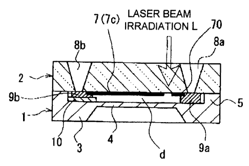
to the drawings. FIG 1 shows a cross-sectional structure of a capacitance
type sensor according to an embodiment of the present invention, while FIG
CA 02561297 2010-04-07
9
2 is a top plan structure of the sensor, in which a glass substrate 2 is
transparent, and a fixed electrode 7 and so on are shown in a see-through
manner. The drawings show a silicon substrate 1 (semiconductor substrate)
as a wafer corresponding to one sensor chip part together with the glass
substrate 2 (insulating substrate), while in an actual manufacturing process,
areas corresponding to the glass substrate 2 are allocated on the surface of a
large glass substrate. This similarly applies to the silicon substrate 1.
Before anodic bonding to bond both substrates, the fixed electrode 7
and lead portions 7c having a predetermined pattern shape are formed at the
same time by evaporation or sputtering on the bonding face-side surface of
the glass substrate 2. When this fixed electrode 7 is formed, an
equipotential wiring 70 is formed at the same time which is led from the
fixed electrode 7 and is a short-circuit conductive pattern to short-circuit
the
fixed electrode 7 and a movable electrode (first step). The equipotential
wiring 70 is formed inside the bonding area, namely in the fixed electrode 7
of the glass substrate 2. The equipotential wiring 70 can be formed by only
changing the pattern shape of evaporating/sputtering a given metal on the
surface of the glass substrate 2. Meanwhile, a support mounting 3 and a
pressure-sensing portion 4 are formed on the silicon substrate 1 by etching.
The bonding face-side surface of the silicon substrate 1 including the
pressure-sensing portion 4 serves as a movable electrode.
Such silicon substrate 1 and glass substrate 2 are contacted with their
relative positions being aligned together. Here, mutually facing peripheral
areas (referred to as bonding areas) 5 of the silicon substrate 1 and glass
substrate 2 are contacted for anodic bonding, and both substrates have an
CA 02561297 2010-04-07
anodic bonding voltage applied therebetween so as to be integrated by
anodic bonding (second step) as will be described in detail later. The
equipotential wiring 70 is cut and removed after the anodic bonding as
shown by a wiring cutting location C (third step). The equipotential wiring
5 70 serves to electrically connect the fixed electrode 7 of the glass
substrate 2
to the movable electrode of the silicon substrate 1, and is used as a
countermeasure to discharge in anodic bonding.
Two through-holes 8a, 8b for the movable electrode and the fixed
electrode are formed at predetermined positions in, and penetrate up and
10 down through, the glass substrate 2. The silicon substrate 1 has formed
thereon a conductive film 9a electrically connected to the movable electrode
so as to be exposed to the bottom portion of the through-hole 8a, and also
has formed thereon a conductive film 9b electrically connected to the fixed
electrode 7 through its lead portions 7c so as to be exposed to the bottom
portion of the through-hole 8b. This conductive film 9b is formed on an
insulating film 10 for insulation from the silicon substrate 1. A sensor
signal is output from the conductive films 9a, 9b to an external circuit via
the
through-holes 8a, 8b. The through-holes each have an inner wall surface
with a conductive film formed thereon, and are respectively electrically
connected to conductive thin films formed mutually separately on the
surface of the glass substrate 2.
This kind of pressure sensor of electrostatic capacitance type changes
a capacitance gap 6 with a pressure applied to the pressure-sensing portion 4.
Assuming that this gap length is d, and that the area of the fixed electrode 7
is S, a capacitance C between both electrodes is to output a change according
CA 02561297 2010-04-07
11
to C =c oS/d.
Next, anodic bonding between the silicon substrate 1 and glass
substrate 2 of the capacitance type sensor will be described in detail. For
anodic bonding, an anode of a power supply for anodic bonding is connected
to the silicon substrate 1, and further a cathode of the power supply for
anodic bonding is connected to the glass substrate 2, so as to apply a
predetermined voltage between both electrodes. Thereby, a current is
caused to flow between the silicon substrate 1 and glass substrate 2, contact
portions of both of which, namely the peripheral areas (bonding area) 5 in
lo the present example, are bonded and integrated (anodic bonding). At this
time, the fixed electrode 7 and the movable electrode are short-circuited by
the equipotential wiring 70 to be equipotential, so that it is unlikely for a
potential difference to be generated therebetween. This prevents discharge
between the electrodes in the anodic bonding, and thus prevents the
electrodes from being alloyed and thereby fusion-bonded together upon the
discharge, whereby the anodic bonding is secured.
After the anodic bonding, the equipotential wiring 70 is cut. For
this purpose, a laser beam irradiation L (arrow in FIG 1) is used. A laser
beam, using CO2, YAG or the like, is allowed to pass from the glass
substrate 2 through the glass, and is irradiated to the wiring cutting
location
C of the equipotential wiring 70, thereby cutting the equipotential wiring 70.
In this way, a sensor having desired characteristics can be obtained.
Next, another method of removing the equipotential wiring 70
following the anodic bonding in the capacitance type sensor will be
described. As shown in FIG 3, a DC bias power supply 12 is connected so
CA 02561297 2010-04-07
12
as to cause a current to flow in the equipotential wiring 70, and the current
flow based on this voltage application causes the equipotential wiring 70 to
generate heat so as to be melted and cut. The voltage is applied between
the conductive films 9a, 9b exposed at the bottom portions of the respective
through-holes 8a, 8b which are provided in the glass substrate 2 for the
movable electrode and the fixed electrode. The applied voltage had better
be gradually increased to increase the probability of cutting at a constant
location.
In the method of removing the equipotential wiring 70 by the
lo above-described voltage application, it is also possible, as shown in FIG.
4,
to use the through-holes 8a, 8b of the glass substrate 2 as voltage
application
terminals. Conductive films 13a, 13b are formed on inner wall surfaces of
the through-holes 8a, 8b, while conductive film portions 14a, 14b which are
electrically connected to the conductive films 9a, 9b on the silicon substrate
1 via the conductive films 13a, 13b are formed on the glass substrate 2,
allowing the conductive film portions 14a, 14b to serve as the voltage
application terminals. The step of forming the conductive layers 13a, 13b
on the inner wall surfaces of the through-holes can be performed either
before or after the anodic bonding.
In either the process of cutting the equipotential wiring 70 using the
laser beam irradiation or the process of cutting the equipotential wiring 70
using the voltage application as described above, it is preferable to form, as
shown in FIG 5, a reduced-width portion D of the equipotential wiring 70
which is around the wiring cutting location and which is reduced in the
width of the wiring pattern. The reduced-width portion D, which is thus
CA 02561297 2010-04-07
13
partially present in the equipotential wiring 70, facilitates recognizing the
target location of a laser beam spot for cutting in the case of the cutting
process using a laser, and increases the electrical resistance at the portion
of
the reduced wiring width in the case of the cutting process using voltage
application, thereby making it possible to stabilize the cutting location.
While the above has shown an embodiment with an equipotential
wiring 70 formed on a glass substrate 2 in a capacitance type sensor, a
capacitance type sensor of another embodiment with one formed on a silicon
substrate 1 will be described hereinafter with reference to FIG 6 and FIG 7.
An equipotential wiring 71 according to this embodiment is formed on a
silicon substrate 1 so as to electrically connect a conductive film 9b for a
fixed electrode to a movable electrode of the silicon substrate 1 (first
step).
This equipotential wiring 71 makes a fixed electrode 7 equipotential to the
movable electrode. This prevents discharge between the electrodes in
anodic bonding similarly as in the above-described embodiment, whereby
secure anodic bonding is performed.
After the anodic bonding (second step), this equipotential wiring 71
is cut. The equipotential wiring 71 is cut by applying a laser beam
irradiation L to a wiring cutting location C from a glass substrate 2 through
the glass (third step).
Although not shown, the equipotential wiring 71 following the
anodic bonding can be cut either by applying a DC voltage to the conductive
films for the movable electrode and fixed electrode similarly as in the above
FIG 3, or by using through-holes of the glass substrate 2 similarly as in FIG.
4. Furthermore, similarly as in the above, it is preferable to reduce a wiring
CA 02561297 2010-04-07
14
width around the wiring cutting location of the equipotential wiring 71.
Although various embodiments of the present invention have been
described above, its various modifications are possible without being limited
to the structures of the above-described embodiments, such that examples of
the MEMS device to be mentioned as an object to which it is to be applied
are electrostatic capacitance type pressure sensor, electrostatic capacitance
type angular velocity sensor and others such as piezoelectric type
pressure/acceleration/angular velocity sensor and MEMS mechanical relay.
Furthermore, the glass substrate 2 is only required to be of an insulating
lo substrate material, in which glass and other transparent materials that
pass a
laser beam can be used therefor. Silicon and others such as GaAs and Ge
can be used for the silicon substrate 1. Materials which can be used for the
fixed electrode/conductive films are Cr, Al and others such as Au, Ag, Cu, Pt
and Ti.
Further, the present application is based on Japanese Patent
Application 2005-007784.