Language selection

Search

Patent 2561572 Summary

Third-party information liability

Some of the information on this Web page has been provided by external sources. The Government of Canada is not responsible for the accuracy, reliability or currency of the information supplied by external sources. Users wishing to rely upon this information should consult directly with the source of the information. Content provided by external sources is not subject to official languages, privacy and accessibility requirements.

Claims and Abstract availability

Any discrepancies in the text and image of the Claims and Abstract are due to differing posting times. Text of the Claims and Abstract are posted:

  • At the time the application is open to public inspection;
  • At the time of issue of the patent (grant).
(12) Patent Application: (11) CA 2561572
(54) English Title: PHASE FREQUENCY DETECTOR WITH A NOVEL D FLIP FLOP
(54) French Title: DETECTEUR DE FREQUENCE DE PHASE AVEC NOUVELLE BASCULE DE TYPE D
Status: Dead
Bibliographic Data
Abstracts

English Abstract


Methods, systems and components for use with or as a phase frequency detector.
The phase frequency detector stretches its output pulse, allowing the detector
to operate in a more linear region. As part of the invention, a new
configuration for a D type flip flop is also disclosed. In one embodiment, the
D type flip flop triggers at both the rising and the falling edges of the
reference input, allowing a lower frequency input to be used while having the
advantages of a higher frequency.


French Abstract

Cette invention se rapporte à des procédés, des systèmes et des composants conçus pour être utilisés avec un détecteur de fréquence de phase ou comme détecteur de fréquence de phase. Ce détecteur de fréquence de phase étale son impulsion de sortie, ce qui lui permet de fonctionner dans une zone plus linéaire. Faisant partie de cette invention, une nouvelle configuration pour une bascule de type D est également présentée. Dans un mode de réalisation, la bascule de type D se déclenche à la fois sur le front montant et sur le front descendant de l'entrée de référence, ce qui permet d'utiliser une entrée de fréquence inférieure, tout en profitant de l'avantage d'une fréquence supérieure.

Claims

Note: Claims are shown in the official language in which they were submitted.


What is claimed is:

1. A D-type flip flop comprising:
- a first FET (field effect transistor) receiving an input signal at its gate
terminal;
- a delay element also receiving said input signal, said delay element
outputting a delayed logical inverse of said input signal;
- a second FET receiving an output of said delay element at its gate
terminal, a drain terminal of said second FET being coupled to a source
terminal
of said first FET, a source terminal of said second FET being coupled to a
relative ground;
- a reset FET coupled to said relative ground by way of its source terminal,
a drain terminal of said reset FET being coupled to a junction node, a gate
terminal of said reset FET being coupled to an external reset input;
- a third FET coupled by way of its source terminal to said junction node, a
drain terminal of said third FET being coupled to a power supply, a gate
terminal
of said third FET being coupled a drain terminal of said first FET;
- a fourth FET coupled to said drain terminal of said first FET by way of a
source terminal of said fourth FET, a drain terminal of said fourth FET being
coupled to said power supply and a gate terminal of said fourth FET being
coupled to said junction node,
wherein
- an output of said flip flop is tapped from said junctions node;
- said first, second and reset FETs are of the same type of FET; and
- said third and fourth FETs are of the same type of FET.

2. A D type flip flop according to claim 1 wherein said flip flop is used in a
phase
frequency detector.

3. A D type flip flop according to claim 1 further comprising:
- a first branch delay element receiving said input signal and outputting a


11


delayed logical inverse of said output of said first branch delay element;
- a fifth FET coupled to said drain terminal of said first FET by way of a
drain terminal of said fifth FET, a gate terminal of said fifth FET receiving
an
output of said first brand delay element;
- a sixth FET coupled to fifth FET, a drain terminal of said sixth FET being
coupled to a source terminal of said fifth FET, a source terminal of said
sixth FET
being coupled to said relative ground, a gate terminal of said sixth FET being
coupled to an output of said second branch delay element.

4. A phase-frequency detector circuit comprising:
- a first D flip flop receiving a reference input;
- a second D flip flop receiving a divider input;
- a first NAND gate receiving a first select input and said divider input;
- a first NOT gate receiving an output of said first NAND gate;
- a NOR gate receiving an output of said first NOT gate and an output of
said first D flip flop;
- a second NOT gate receiving an output of said NOR gate and producing
a first output of said detector circuit;
- a second NAND gate receiving said output of said first D flip flop gate
and an output of said second D flip flop;
- a third NOT gate receiving an output of said fourth NAND gate, an output
of said third NOT gate being received as a reset input to both said first and
second D flip flops.

5. A phase frequency detector circuit comprising:
- a first D flip flop receiving a reference input;
- a second D flip flop receiving a divider input;
- a first NAND gate receiving a select input and said divider input;
- a second NAND gate receiving an output of said first NAND gate and a
logical inverse of an output of said second D flip flop;
- a first NOT gate receiving an output of said second NAND gate and
producing an output of said detector circuit;


12


- a third NAND gate receiving an output of said first D flip flop and said
output of said second D flip flop;
- a second NOT gate receiving an output of said third NAND gate, an
output of said second NOT gate being received as a reset input to both said
first
and second D flip flops.

6. A phase frequency detector circuit comprising:
- a first D flip flop receiving a reference input;
- a second D flip flop receiving a divider input;
- a first NAND gate receiving a first select input and said divider input;
- a first NOT gate receiving an output of said first NAND gate;
- a NOR gate receiving an output of said first NOT gate and an output of
said first D flip flop;
- a second NOR gate receiving an output of said NOR gate and producing
first output of said detector circuit;
- a second NAND gate receiving a second select input and said divider
input;
- a third NAND gate receiving an output of said first D flip flop and an
output of said second D flip flop;
- a third NOT gate receiving an output of said third NAND gate, an output
of said third NOT gate being received as a reset input to both said first and
second D flip flops;
- a fourth NAND gate receiving a second select input and said divider
input;
- a fifth NAND gate receiving an output of said first NAND gate and a
logical inverse of said output of said second D flip flop;
- a fourth NOT gate receiving an output of said fifth NAND gate and
producing a second output of said detector circuit.

7. A phase frequency detector according to claim 4 wherein said first D Flip
flop
comprises:
- a first FET (field effect transistor) receiving an input signal at its gate


13


terminal;
- a delay element also receiving said input signal, said delay element
outputting a delayed logical inverse of said input signal;
- a second FET receiving an output of said delay element at its gate
terminal, a drain terminal of said second FET being coupled to a source
terminal
of said first FET, a source terminal of said second FET being coupled to a
relative ground;
- a reset FET coupled to said relative ground by way of its source terminal,
a drain terminal of said reset FET being coupled to a junction node, a gate
terminal of said reset FET being coupled to an external reset input;
- a third FET coupled by way of its source terminal to said junction node, a
drain terminal of said third FET being coupled to a power supply, a gate
terminal
of said third FET being coupled a drain terminal of said first FET;
- a fourth FET coupled to said drain terminal of said first FET by way of a
source terminal of said fourth FET, a drain terminal of said fourth FET being
coupled to said power supply and a gate terminal of said fourth FET being
coupled to said junction node,
wherein
- an output of said flip flop is tapped from said junctions node;
- said first, second and reset FETs are of the same type of FET; and
- said third and fourth FETs are of the same type of FET.

8. A phase frequency detector according to claim 7 wherein said first D Flip
flop
comprises:
- a first branch delay element receiving said input signal and outputting a
delayed
logical inverse of said output of said first branch delay element;
- a fifth FET coupled to said drain terminal of said first FET by way of a
drain terminal of said fifth FET, a gate terminal of said fifth FET receiving
an
output of said first brand delay element;
- a sixth FET coupled to fifth FET, a drain terminal of said sixth FET being
coupled to a source terminal of said fifth FET, a source terminal of said
sixth FET


14


being coupled to said relative ground, a gate terminal of said sixth FET being
coupled to an output of said second branch delay element.

9. A phase frequency detector according to claim 5 wherein said second D flip
flop comprises:
- a first FET (field effect transistor) receiving an input signal at its gate
terminal;
- a delay element also receiving said input signal, said delay element
outputting a delayed logical inverse of said input signal;
- a second FET receiving an output of said delay element at its gate
terminal, a drain terminal of said second FET being coupled to a source
terminal
of said first FET, a source terminal of said second FET being coupled to a
relative ground;
- a reset FET coupled to said relative ground by way of its source terminal,
a drain terminal of said reset FET being coupled to a junction node, a gate
terminal of said reset FET being coupled to an external reset input;
- a third FET coupled by way of its source terminal to said junction node, a
drain terminal of said third FET being coupled to a power supply, a gate
terminal
of said third FET being coupled a drain terminal of said first FET;
- a fourth FET coupled to said drain terminal of said first FET by way of a
source terminal of said fourth FET, a drain terminal of said fourth FET being
coupled to said power supply and a gate terminal of said fourth FET being
coupled to said junction node,
wherein
- an output of said flip flop is tapped from said junctions node;
- said first, second and reset FETs are of the same type of FET; and
- said third and fourth FETs are of the same type of FET.

10. A phase frequency detector according to claim 5 wherein said second D flip
flop comprises:
- a first branch delay element receiving said input signal and outputting a
delayed


15


logical inverse of said output of said first branch delay element;
- a fifth FET coupled to said drain terminal of said first FET by way of a
drain terminal of said fifth FET, a gate terminal of said fifth FET receiving
an
output of said first brand delay element;
- a sixth FET coupled to fifth FET, a drain terminal of said sixth FET being
coupled to a source terminal of said fifth FET, a source terminal of said
sixth FET
being coupled to said relative ground, a gate terminal of said sixth FET being
coupled to an output of said second branch delay element.

11. A phase frequency detector according to claim 6 wherein at least one of
said
first D flip flop and said second D flip flop comprises:
- a first FET (field effect transistor) receiving an input signal at its gate
terminal;
- a delay element also receiving said input signal, said delay element
outputting a delayed logical inverse of said input signal;
- a second FET receiving an output of said delay element at its gate
terminal, a drain terminal of said second FET being coupled to a source
terminal
of said first FET, a source terminal of said second FET being coupled to a
relative ground;
- a reset FET coupled to, said relative ground by way of its source terminal,
a drain terminal of said reset FET being coupled to a junction node, a gate
terminal of said reset FET being coupled to an external reset input;
- a third FET coupled by way of its source terminal to said junction node, a
drain terminal of said third FET being coupled to a power supply, a gate
terminal
of said third FET being coupled a drain terminal of said first FET;
- a fourth FET coupled to said drain terminal of said first FET by way of a
source terminal of said fourth FET, a drain terminal of said fourth FET being
coupled to said power supply and a gate terminal of said fourth FET being
coupled to said junction node,
wherein
- an output of said flip flop is tapped from said junctions node;
- said first, second and reset FETs are of the same type of FET; and


16


- said third and fourth FETs are of the same type of FET.

12. A phase frequency detector according to claim 11 wherein at least one of
said first D flip flop and said second D flip flop comprises:
- a first branch delay element receiving said input signal and outputting a
delayed
logical inverse of said output of said first branch delay element;
- a fifth FET coupled to said drain terminal of said first FET by way of a
drain terminal of said fifth FET, a gate terminal of said fifth FET receiving
an
output of said first brand delay element;
- a sixth FET coupled to fifth FET, a drain terminal of said sixth FET being
coupled to a source terminal of said fifth FET, a source terminal of said
sixth FET
being coupled to said relative ground, a gate terminal of said sixth FET being
coupled to an output of said second branch delay element.

13. A phase frequency detector comprising:
- at least two D flip flops;
- a plurality of logic gates, at least one of said logic gates being coupled
to
at least one of said D flip flops,
wherein
- at least one of said at least two D flip flops comprises:
- a first FET (field effect transistor) receiving an input signal at its gate
terminal;
- a delay element also receiving said input signal, said delay element
outputting a delayed logical inverse of said input signal;
- a second FET receiving an output of said delay element at its gate
terminal, a drain terminal of said second FET being coupled to a source
terminal
of said first FET, a source terminal of said second FET being coupled to a
relative ground;
- a reset FET coupled to said relative ground by way of its source terminal,
a drain terminal of said reset FET being coupled to a junction node, a gate
terminal of said reset FET being coupled to an external reset input;


17


- a third FET coupled by way of its source terminal to said junction node, a
drain terminal of said third FET being coupled to a power supply, a gate
terminal
of said third FET being coupled a drain terminal of said first FET;
- a fourth FET coupled to said drain terminal of said first FET by way of a
source terminal of said fourth FET, a drain terminal of said fourth FET being
coupled to said power supply and a gate terminal of said fourth FET being
coupled to said junction node,
wherein
- an output of said flip flop is tapped from said junctions node;
- said first, second and reset FETs are of the same type of FET; and
- said third and fourth FETs are of the same type of FET.

14. A phase frequency detector according to claim 13 wherein said at least one
of said at least two D flip flops further comprises:
- a first branch delay element receiving said input signal and outputting a
delayed logical inverse of said output of said first branch delay element;
- a fifth FET coupled to said drain terminal of said first FET by way of a
drain terminal of said fifth FET, a gate terminal of said fifth FET receiving
an
output of said first brand delay element;
- a sixth FET coupled to fifth FET, a drain terminal of said sixth FET being
coupled to a source terminal of said fifth FET, a source terminal of said
sixth FET
being coupled to said relative ground, a gate terminal of said sixth FET being
coupled to an output of said second branch delay element.

15. A phase frequency detector according to claim 13 wherein said detector
receives at least one select input, said at least one select input determining
which output pulses of said detector is extended.

16. A phase frequency detector according to claim 13 wherein at least one of
said at least two D flip flops has for an input frequency of n, a output
frequency of
2n.


18


17. A phase frequency detector circuit according to claim 6 wherein said first
and
second select inputs determine which pulse outputs of said detector circuit
are to
be extended.


19

Description

Note: Descriptions are shown in the official language in which they were submitted.


CA 02561572 2006-09-28
WO 2005/096501 PCT/CA2004/000511
PHASE FREQUENCY DETECTOR WITH A NOVEL D FLIP FLOP
Field of the invention
The present invention relates to electronics and, more specifically, relates
to a phase frequency detector circuit employing a novel D flip flop element.
Background to the Invention
The recent revolution in telecommunications has led to a corresponding
revolution in electronics. Wireless communications devices are now as
plentiful
as the rotary telephone of yesteryears. One key component of many wireless
circuits is the delta sigma controlled fractional N frequency synthesizer.
Such a
circuit allows for the synthesizing of almost any required signal frequency.
As
part of this component, a phase frequency detector (PFD) receives an input
reference signal with a known frequency and a variable input signal, known as
a
divider input, with a variable frequency determined by dividing a VCO (voltage
controlled oscillator) frequency. The PFD outputs a signal that is
proportional to
the difference in phase between the input reference signal and the divider
input.
This output can then be used to increase or decrease the VCO frequency to
minimize the phase difference. This feedback arrangement is called a phase
lock loop or a PLL.
Current PFD designs suffer from what is commonly termed a "deadzone".
When the frequency synthesizer is in lock, the phase difference between the
reference and the divider input is very close to zero. Thus, the output (or
outputs
as the PFD may have more than one output) should not be active or, if they
are,
the pulses produced should be very narrow. For small phase errors close to
zero, due to delays and uncontrollable circumstances, it is not possible to
create
a complete pulse at the output of the PFD. This results in a flat or non-
linear
section in the PFD transfer curve normally termed a deadzone. While not very
serious for integer-N synthesizers, this can result in increased fractional-N
spur
levels for delta sigma controlled fractional-N frequency synthesizers.
1


CA 02561572 2006-09-28
WO 2005/096501 PCT/CA2004/000511
As such, there is therefore a need for systems and components which
avoid the above problems. It is therefore an object of the present invention
to
mitigate if not overcome the shortcomings of the prior art.
Summar~of the Invention
The present invention provides methods, systems and components for
use with or as a phase frequency detector. The phase frequency detector
stretches one of its output pulses, forcing the PLL to operate in a region
where
the phase difference between the divider and the reference is no close to
zero.
This allows the detector to operate in a more linear region. As part of the
invention, a new configuration for a D type flip flop is also disclosed. In
one
embodiment, the D type flip flop triggers at both the rising and the falling
edges of
the reference input, allowing a lower frequency input to be used while having
the
advantages of a higher frequency.
In a first aspect, the present invention provides a D-type flip flop
comprising:
- a first FET (field effect transistor) receiving an input signal at its gate
terminal;
- a delay element also receiving said input signal, said delay element
outputting a delayed logical inverse of said input signal;
- a second FET receiving an output of said delay element at its gate
terminal, a drain terminal of said second FET being coupled to a source
terminal
of said first FET, a source terminal of said second FET being coupled to a
relative ground;
- a reset FET coupled to said relative ground by way of its source terminal,
a drain terminal of said reset FET being coupled to a junction node, a gate
terminal of said reset FET being coupled to an external reset input;
- a third FET coupled by way of its source terminal to said junction node, a
drain terminal of said third FET being coupled to a power supply, a gate
terminal
of said third FET being coupled a drain terminal of said first FET;
- a fourth FET coupled to said drain terminal of said first FET by way of a
source terminal of said fourth FET, a drain terminal of said fourth FET being
2


CA 02561572 2006-09-28
WO 2005/096501 PCT/CA2004/000511
coupled to said power supply and a gate terminal of said fourth FET being
coupled to said junction node,
wherein
- an output of said flip flop is tapped from said junctions node;
- said first, second and reset FETs are of the same type of FET; and
- said third and fourth FETs are of the same type of FET.
In a second embodiment the present invention provides a phase-
frequency detector circuit comprising:
- a first D flip flop receiving a reference input;
- a second D flip flop receiving a divider input;
- a first NAND gate receiving a first select input and said divider input;
a first NOT gate receiving an output of said first NAND gate;
- a NOR gate receiving an output of said first NOT gate and an output of
said first D flip flop;
- a second NOT gate receiving an output of said NOR gate and producing
a first output of said detector circuit;
- a second NAND gate receiving said output of said first D flip flop gate
and an output of said second D flip flop;
- a third NOT gate receiving an output of said fourth NAND gate, an output
of said third NOT gate being received as a reset input to both said first and
second D flip flops.
In a third embodiment, the present invention provides a phase frequency
detector circuit comprising:
- a first D flip flop receiving a reference input;
- a second D flip flop receiving a divider input;
- a first NAND gate receiving a select input and said divider input;
- a second NAND gate receiving an output of said first NAND gate and a
logical inverse of an output of said second D flip flop;
- a first NOT gate receiving an output of said second NAND gate and
producing an output of said detector circuit;
- a third NAND gate receiving an output of said first D flip flop and said
output of said second D flip flop;
3


CA 02561572 2006-09-28
WO 2005/096501 PCT/CA2004/000511
- a second NOT gate receiving an output of said third NAND gate, an
output of said second NOT gate being received as a reset input to both said
first
and second D flip flops.
In yet another embodiment the present invention provides a phase
frequency detector circuit comprising:
- a first D flip flop receiving a reference input;
- a second D flip flop receiving a divider input;
- a first NAND gate receiving a first select input and said divider input;
- a first NOT gate receiving an output of said first NAND gate;
- a NOR gate receiving an output of said first NOT gate and an output of
said first D flip flop;
- a second NOR gate receiving an output of said NOR gate and producing
first output of said detector circuit;
- a second NAND gate receiving a second select input and said divider
input;
- a third NAND gate receiving an output of said first D flip flop and an
output of said second D flip flop;
- a third NOT gate receiving an output of said third NAND gate, an output
of said third NOT gate being received as a reset input to both said first and
second D flip flops;
- a fourth NAND gate receiving a second select input and said divider
input;
- a fifth NAND gate receiving an output of said first NAND gate and a
logical inverse of said output of said second D flip flop;
- a fourth NOT gate receiving an output of said fifth NAND gate and
producing a second output of said detector circuit.
In a fifth embodiment the present invention provides, a phase frequency
detector comprising:
- at least two D flip flops;
- a plurality of logic gates, at least one of said logic gates being coupled
to
at least one of said D flip flops,
wherein
4


CA 02561572 2006-09-28
WO 2005/096501 PCT/CA2004/000511
- at least one of said at least two D flip flops comprises:
- a first FET (field effect transistor) receiving an input signal at its gate
terminal;
- a delay element also receiving said input signal, said delay element
outputting a delayed logical inverse of said input signal;
- a second FET receiving an output of said delay element at its gate
terminal, a drain terminal of said second FET being coupled to a source
terminal
of said first FET, a source terminal of said second FET being coupled to a
relative ground;
- a reset FET coupled to said relative ground by way of its source terminal,
a drain terminal of said reset FET being coupled to a junction node, a gate
terminal of said reset FET being coupled to an external reset input;
- a third FET coupled by way of its source terminal to said junction node, a
drain terminal of said third FET being coupled to a power supply, a gate
terminal
of said third FET being coupled a drain terminal of said first FET;
- a fourth FET coupled to said drain terminal of said first FET by way of a
source terminal of said fourth FET, a drain terminal of said fourth FET being
coupled to said power supply and a gate terminal of said fourth FET being
coupled to said junction node,
wherein
- an output of said flip flop is tapped from said junctions node;
- said first, second and reset FETs are of the same type of FET; and
- said third and fourth FETs are of the same type of FET.
Brief Description of the Drawings
A better understanding of the invention will be obtained by considering the
detailed description below, with reference to the following drawings in which:
Figure 1 illustrates a phase frequency detector according to the prior art;
Figure 2 illustrates a phase frequency detector according to one aspect of the
invention;
Figure 3 illustrates a D flip-flop which may be used in the phase frequency
detector of Figure 2; and
5


CA 02561572 2006-09-28
WO 2005/096501 PCT/CA2004/000511
Figure 4 illustrates a variant of the D flip-flop of Figure 3
Detailed Description
Referring to Figure 1, a phase frequency detector 10 according to the prior
art is illustrated. Two D type flip flops 20, 30 are illustrated with flip
flop 20
receiving a reference input 40 and flip flop 30 receiving a variable frequency
input
50 known as a divider input. As is well known in the art, the PFD 10 seeks to
minimize the phase difference between the reference input 40 and the divider
input 50. The outputs 60, 70 can be used as a feedback to the VCO. Output 60,
known as the pump up output (output Q of D flip flop 20), is high when the
reference edge arrives before the divider edge arrives. Thus, in this case,
the
VCO signal must be "pumped up" or increased to match the divider input.
Similarly, if the divider edge arrives first, the other output, known as the
pump
down output (output Qe of D flip flop 30), is high. This means that the
reference
frequency must be reduced to match the divider input. To provide flexibility
in the
logic used, each output has a corresponding logical inverse as part of the
output.
Output 60A (PUB or pump up bar or output Qe) is the logical inverse of the
output 60 while output 70A (PDB or pump down bar or output Q) is the logical
inverse of the output 70.
The system is reset after every pulse so the D flip flops 20, 30 may re-
sample the incoming reference and divider inputs. The reset is accomplished
using the NAND gate 80 and NOT gate 90. The NAND gate 80 receives outputs
60, 70 and its output is received by NOT gate 90. The output of NOT gate 90 is
received at the reset ports of the D flip flops 20, 30. Because of delay
through
the gates 80, 90 the reset does not immediately occur, resulting in a finite
pulse
width for the outputs even when the PFD is in lock (i.e. when the reference
frequency and divider input have minimal phase difference). The widths of the
output pulses are proportional to the phase difference between the rising
edges
of the inputs. In an alternative, the NAND gate 80 and NOT gate 90 can be
replaced by a single AND gate. It should be noted for clarity that when
referring
to an output of a d flip flop, this is to mean either Q or Qe and not the
logical
inverse of these outputs.
6


CA 02561572 2006-09-28
WO 2005/096501 PCT/CA2004/000511
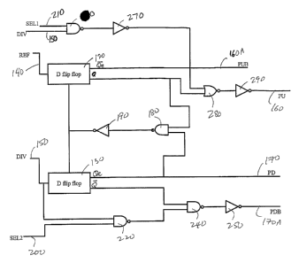
Referring to Figure 2, a novel arrangement for a phase frequency detector
100 is illustrated. Two D flip flops 120, 130 receive a reference input 140
and a
divider input 150. The divider input 150 is a variable frequency input signal
which
is adjusted up or down based on the status of the output signals while
reference
input 160 is a fixed frequency input signal. Much like the system in Figure 1,
the
pump up output 160 has a counterpart logical inverse output pump up bar output
160A. The pump down output 170 similarly has a logical inverse counterpart - a
pump down bar (PDB) output 170A.
The reset arrangement for the system in Figure 2 is similar to that in
Figure 1 - a NAND gate 180 receives outputs 160, 170 and passes its output to
a
NOT gate 190. The output of the NOT gate 190 is received by the reset inputs
of
D flip flops 120, 130.
To select which outputs are to be stretched or which outputs are to have
their pulses extended, select inputs 200, 210 are provided. If select input
200 is
high, then the pump down output 170A is extended while if select input 210 is
high, then the pump up outputs 160 is extended.
The above feature is implemented by properly gating selected outputs of
the D flip flops with the select inputs 200, 210. Select input 200 is
received,
along with the divider input 150, by a NAND gate 220. The output of NAND gate
220 is received, along with the logical inverse 230 of the pump down output
170,
by a NAND gate 240. The output of NAND gate 240 is then received by NOT
gate 250. The output of NOT gate 250 is the extended pump down bar output
170A. The NAND gate 220 may, if desired, be a single NOT gate receiving the
select input 200.
For the extended pump up output 160, the select input 210 is received by
NAND gate 260 along with the divider input 150. The output of NAND gate 260
is received by NOT gate 270, the output of which is received by NOR gate 280.
NOT gate 280 also receives the pump up output of D flip flop 120. The result
of
NOR gate 280 is NOT gated (NOT gate 290) to produce the pump up output 160
of the phase frequency detector 100.
It should be noted that while the embodiment in Figure 2 extends the
pulse of the pump up output 160 and of the pump down bar output 170A, a
7


CA 02561572 2006-09-28
WO 2005/096501 PCT/CA2004/000511
similar arrangement, but with different gating connections, can provide
extension
of the pulses of the other outputs. The logic behind the embodiment
illustrated in
Figure 2 is that the divider output is OR'd with either the pump up output or
the
pump down bar output of the detector. The two select inputs are used to
control
which of the outputs get stretched or extended. If the pump up output is
stretched or extended, feedback will similarly extend or stretch the other
output
(pump down bar output) to compensate. In a similar manner, if the pump down
bar output is extended, the pump up output will be extended as well to
compensate. This arrangement introduces a DC phase offset and the loop does
not lock at zero degrees phase offset but rather at an offset controlled by
the
divider pulse width. The phase frequency detector can thus now operate in a
more linear region.
It should further be noted that while Figure 2 illustrates two select inputs
200, 210, the invention may be implemented as having only one select input and
as extending only one of the output pulses. If the implementation only
required
extending the output pulse 160, then gates 220, 240, 250 need not be
implemented. Similarly, if only the output pulse 170A needs to be extended,
then
gates 260, 270, 280, 290 need not be implemented. In these two alternative
embodiments, the sole select input (either of select inputs 200, 210 as the
case
may be) will still extend the relevant output pulse.
Referring to Figure 3, a structure for a novel D flip flop which may be used
in the phase frequency detector of Figure 2 is illustrated. An input 300 to
the D
flip flop 310 is received by a NOT gate 320 (a delay element) and a gate of
FET
(field effect transistor) 330. The NOT gate output is received by the gate of
a
FET 340. The source terminal of FET 340 is coupled to Vss 350 while the drain
terminal is coupled to the source terminal of FET 330. The drain terminal of
FET
330 is coupled to the gate terminal of FET 360. The source terminal of FET 360
is coupled to a junction node 370 from which the output 380 of the D flip flop
310
is tapped. Also coupled to the drain terminal of FET 330 is the source
terminal of
FET 390. The drain terminal of FET 390 is coupled to Vpp 400. Vop 400 is also
coupled to the drain terminal of FET 360.
The junction node 370 serves as a coupling point for the gate terminal of
8


CA 02561572 2006-09-28
WO 2005/096501 PCT/CA2004/000511
FET 390 and a drain terminal of a reset FET 410. The reset FET 410 has a gate
terminal which receives a reset input to the D flip flop 310 and a source
terminal
coupled to Vss 350.
In the phase frequency detector of Figure 2, the D flip flop 310 of Figure 3
would receive the reference input 140 at the input terminal 300. This
reference
input is applied to FET 330 and a delayed and inverted version is applied to
FET
340. When the rising edge of the reference input occurs, FET 330 pulls the
left
side of the latch (a cross coupled latch formed by FETs 390, 360) low. In
order
to make the latch edge sensitive, the falling edge of the inverted input
reference
signal, applied to FET 340, falls low afterwards and turns off the left branch
of the
latch.
It should be noted that, as can be seen in Figure 3, the FETs 330, 340,
410 are n channel FETs while FETs 360, 390 are p channel FETs. While
MOSFETs (metal oxide semiconductor field effect transistors) are contemplated
for implementation, other types of FETs, such as JFETs, may be used.
The D type flip flop of Figure 3 may be modified to be sensitive to both
rising and falling edges of the reference input. The D type flip flop of
Figure 3 is
only sensitive to and therefore only reacts to the rising edge of the input.
With
the addition of some FETs and some gating, the flip flop can respond to both
rising and falling edges of the input. This would allow a lower input
frequency to
be used while achieving the performance of a higher input frequency,
Referring to Figure 4, the D type flip flop 500 is similar to that in Figure 3
except with the addition of branch delay elements (NOT gates) 510, 520 and
FETs 530, 540. The delay element 510 receives the input 300 and the output of
this NOT gate 510 is received by the gate terminal of FET 540. The output of
NOT gate 510 is also received by delay element (NOT gate) 520, the output of
which is received by the gate terminal of FET 530. The source terminal of FET
530 is coupled to relative ground (Vss) 350 and the drain terminal of FET 530
is
coupled to the source terminal of FET 540. The drain terminal of FET 540 is
coupled to the drain terminal of FET 330.
The D flip flop of Figure 4 may also be used in the phase frequency
detector of Figure 2. Using the D flip flop of Figure 4 will allow a doubling
of the
9


CA 02561572 2006-09-28
WO 2005/096501 PCT/CA2004/000511
input frequency. Thus, an input reference frequency of n will have the same
effect is if an input frequency of 2n was used.
A person understanding this invention may now conceive of alternative
structures and embodiments or variations of the above all of which are
intended
to fall within the scope of the invention as defined in the claims that
follow.

Representative Drawing
A single figure which represents the drawing illustrating the invention.
Administrative Status

For a clearer understanding of the status of the application/patent presented on this page, the site Disclaimer , as well as the definitions for Patent , Administrative Status , Maintenance Fee  and Payment History  should be consulted.

Administrative Status

Title Date
Forecasted Issue Date Unavailable
(86) PCT Filing Date 2004-04-02
(87) PCT Publication Date 2005-10-13
(85) National Entry 2006-09-28
Examination Requested 2009-03-25
Dead Application 2013-04-02

Abandonment History

Abandonment Date Reason Reinstatement Date
2012-04-02 FAILURE TO PAY APPLICATION MAINTENANCE FEE

Payment History

Fee Type Anniversary Year Due Date Amount Paid Paid Date
Registration of a document - section 124 $100.00 2006-09-28
Application Fee $400.00 2006-09-28
Maintenance Fee - Application - New Act 2 2006-04-03 $100.00 2006-09-28
Maintenance Fee - Application - New Act 3 2007-04-02 $100.00 2007-04-02
Registration of a document - section 124 $100.00 2008-03-31
Maintenance Fee - Application - New Act 4 2008-04-02 $100.00 2008-03-31
Request for Examination $800.00 2009-03-25
Maintenance Fee - Application - New Act 5 2009-04-02 $200.00 2009-03-26
Maintenance Fee - Application - New Act 6 2010-04-06 $200.00 2010-03-17
Maintenance Fee - Application - New Act 7 2011-04-04 $200.00 2011-03-25
Owners on Record

Note: Records showing the ownership history in alphabetical order.

Current Owners on Record
KABEN WIRELESS SILICON INC.
Past Owners on Record
KABEN RESEARCH INC.
RILEY, TOM
Past Owners that do not appear in the "Owners on Record" listing will appear in other documentation within the application.
Documents

To view selected files, please enter reCAPTCHA code :


To view images, click a link in the Document Description column. To download the documents, select one or more checkboxes in the first column and then click the "Download Selected in PDF format (Zip Archive)" or the "Download Selected as Single PDF" button.

List of published and non-published patent-specific documents on the CPD .

If you have any difficulty accessing content, you can call the Client Service Centre at 1-866-997-1936 or send them an e-mail at CIPO Client Service Centre.


Document
Description 
Date
(yyyy-mm-dd) 
Number of pages   Size of Image (KB) 
Abstract 2006-09-28 1 56
Claims 2006-09-28 9 353
Drawings 2006-09-28 4 40
Description 2006-09-28 10 465
Representative Drawing 2006-11-24 1 7
Cover Page 2006-11-27 1 35
Drawings 2006-09-29 4 35
Claims 2011-07-28 11 338
Assignment 2008-03-31 3 201
PCT 2006-09-28 5 137
Assignment 2006-09-28 6 223
Prosecution-Amendment 2006-09-28 6 86
Correspondence 2008-03-31 2 83
Correspondence 2008-06-17 1 18
Correspondence 2008-06-17 1 13
Prosecution-Amendment 2009-03-25 1 36
Prosecution-Amendment 2011-07-28 14 415
Prosecution-Amendment 2011-01-28 2 70