Note: Descriptions are shown in the official language in which they were submitted.
CA 02562485 2006-10-11
WO 2005/101398 PCT/IB2005/051165
Optical master substrate with mask layer and nethod to manufacture high-
density relief
structure
The present invention relates to an optical master substrate with mask layer
for
manufacturing a high-density relief structure. Such a relief structure can,
for example, be
used as a stamper for mass-replication of read-only memory (ROM) and pre-
grooved write-
once (R) and rewritabl~e (RE) discs. The invention further relates to a method
of
manufacturing such a high-density relief structure. The invention further
relates to the optical
discs manufactured with the processed optical master substrate.
Optical record carriers have seen an evolutionary increase in the data
capacity
by increasing the numerical aperture of the obj ective lens and a reduction of
the laser
wavelength. The total data capacity was increased from 650 Mbyte (CD, NA=0.45,
~, =780
nm) to 4.7 Gbyte (DVD, NA=0.65, ~,=670 nm) to 25 Gbyte for the Blu-ray Disc
(BD,
NA=0.85, ~,=405 nm). Optical record carriers can be of the type write-once
(R), rewritable
(RE) and read-only memory (ROM). The great advantage of ROM discs is the cheap
mass
replication, and therefore the cheap distribution of content such as audio,
video and other
data. Such a ROM disc is, for example, a polycarbonate substrate with tiny
replicated pits
(holes). The pits in a replicated disc can typically be made with injection
molding or a similar
kind of replication process. The manufacturing of a stamper, as used in such a
replication
process, is known as mastering.
In conventional mastering, a thin photosensitive layer, spin-coated on a glass
substrate, is illuminated with a modulated focused laser beam. The modulation
of the laser
beam causes that some parts of the disc are being exposed by UV light while
the intermediate
areas in between the pits remain unexposed. While the disc rotates, and the
focused laser
beam is gradually pulled to the outer side of the disc, a spiral of
alternating illuminated areas
remains. In a second step, the exposed areas are being dissolved in a so-
called development
process to end up with physical holes inside the photo-resist layer. Alkaline
liquids such as
NaOH and K.OH are used to dissolve the exposed areas. The structured surface
is
subsequently covered with a thin Ni layer. In a galvanic process, this sputter-
deposited Ni
layer is further grown to a thick manageable Ni substrate with the inverse pit
structure. This
CA 02562485 2006-10-11
WO 2005/101398 PCT/IB2005/051165
2
Ni substrate with protruding bumps is separated from the substrate with
unexposed areas and
is called the stamper.
ROM discs contain a spiral of alternating pits and lands representing the
encoded data. A reflection layer (metallic or other kind or material with
different index of
refraction coefficient) is added to facilitate the readout of the information.
In most of the
optical recording systems, the data track pitch has the same order of
magnitude as the size of
the optical readout/write spot to ensure optimum data capacity. Compare for
example the data
track pitch of 320 nm and the 1/e spot radius of 305 nm (1/e is the radius at
which the optical
intensity has reduced to 1/e of the maximum intensity) in case of Blu-ray
Disc. In contrary to
write-once and re-veritable optical record carriers, the pit width in a ROM
disc is typically
half of the pitch between adjacent data tracks. Such small pits are necessary
for optimum
readout. It is well known that ROM discs are readout via phase-modulation,
i.e. the
constructive and destructive interference of light rays. During readout of
longer pits,
destructive interference between light rays reflected from the pit bottom and
reflected form
the adjacent land plateau occurs, which leads to a lower reflection level.
Mastering of a pit structure with pits of approximately half the optical
readout
spot typically requires a laser with a lower wavelength than is used for
readout. For CD/DVD
mastering, the Laser Beam Recorder (LBR) typically operates at a wavelength of
413 nm and
numerical aperture of the objective lens of NA=0.9. For BD mastering, a deep
LTV laser with
257 nm wavelength is used in combination with a high NA lens (0.9 for far-
field and 1.25 for
liquid immersion mastering). In other words, a next generation LBR is required
to make a
stamper for the current optical disc generation. An additional disadvantage of
conventional
photoresist mastering is the cumulative photon effect. The degradation of the
photo-sensitive
compound in the photoresist layer is proportional to the amount of
illumination. The sides of
the focused Airy spot also illuminates the adjacent traces during writing
ofpits in the central
track. This multiple exposure leads to local broadening of the pits and
therefore to an
increased pit noise (fitter). Also for reduction of cross-illumination, an as
small as possible
focused laser spot is required. Another disadvantage of photoresist materials
as used in
conventional mastering is the length of the polymer chains present in the
photoresist.
Dissolution of the exposed areas leads to rather rough side edges due to the
long polymer
chains. In particular in case of pits (for ROM) and grooves (for pre-grooved
substrates for
write-once (R) and rewritable (RE) applications) this edge roughness may lead
to
deterioration of the readout signals of the pre-recorded ROM pits and recorded
R/RE data.
CA 02562485 2006-10-11
WO 2005/101398 PCT/IB2005/051165
3
It is an object of the invention to provide a master substrate with mask layer
for making a high-density relief structure, for example, for mass-replication
of high-density
read-only memory (ROM) and recordable (R/RE) discs with the advantage of a
better signal
quality of the pre-recorded data in ROM discs and a qualitatively better pre-
groove for
improved data recording (R/RE). In particular the use of a mask layer enables
the making of
a deep high-density relief structure, i.e. with a large aspect ratio. An
object of the invention is
further to provide a method of making such a high-density relief structure.
Finally, the
invention discloses optical discs made with the proposed master substrate and
method of
processing such a master substrate.
The object is achieved by providing a master substrate comprising a substrate
layer and a recording stack deposited on the substrate layer, the recording
stack comprising:
- a mask layer,
- an interface layer sandwiched between said mask layer and the substrate,
said mask layer comprising a recording material for forming marks and spaces
representing
an encoded data pattern, said forming of marks by thermal alteration by a
focused laser beam
and said marks having a different phase than the unrecorded material.
Preferred embodiments of the master substrate with mask layer are defined in
the dependent claims. In a preferred embodiment, claimed in claim 2, the
master substrate
comprises a growth-dominated phase-change material, said material is an alloy
comprising at
least two materials of the group of materials containing Ge, Sb, Te, In, Se,
Bi, Ag, Ga, Sn,
Pb, As. In another preferred embodiment, the master substrate comprises a Sb-
Te alloy
material doped with Ge and In as recording material, in particular SbzTe doped
with Ge and
In. In another preferred embodiment, claimed in claim 4, the master substrate
comprises a
Sn-Ge-Sb-alloy material, in particular with the composition Sn18,3 - Gelz.6 -
Sbs9.z. The
claimed phase-change materials lead to so-called re-crystallisation in the
tail of the mark
enabling the further reduction of the channel bit length, and thus the
tangential data density.
The thickness range for the mask layer as claimed in claim 1 is defined in
claim S, namely 2-
50 nm, preferably between 5 and 40 nm.
The preferred materials for the interface layer are claimed in claim 6, 7 and
8.
Claim 6 discloses the use of dielectric materials, such as ZnS-SiOz, A1z03,
SiOz, Si3N4, as
interface in the master substrate as claimed in claim 1. Claim 7 discloses the
use of organic
materials of the group dye materials containing phthalo-cyanine, cyanine and
AZO dyes, as
interface layer in the master substrate. Claim 8 discloses the use of organic
photoresist
CA 02562485 2006-10-11
WO 2005/101398 PCT/IB2005/051165
4
materials selected from the group Diazonaphthoquinone-based resists as
interface layer (11).
The preferred thickness of the interface ranges from 5 nm to 200 nm, in
particular between
20 and 110 nm, and is disclosed in claim 9.
In a preferred embodiment, the recording stack of the master substrate with
mask layer as claimed in claim 1, further comprises a protection layer
adjacent the mask layer
at a side most remote from the substrate. The preferred thickness of this
protection layer (81),
disclosed in claim 11, is between 2 and 50 nm, in particular between 5 and 30
nm. The
preferred materials are disclosed in claim 12 and 13. Claim 12 proposes the
use of dielectric
materials such as ZnS-Si02, A1203, Si02, S13N4, TaaO. Claim 13 proposes the
use of organic
photoresist materials, in particular selected from the group
Diazonaphthoquinone-based
resists. Furthermore, the use of soluble organic materials, such as PMMA is
disclosed. The
protection layer is particularly advantageous to prevent large scale migration
of molten
phase-change material. This effect will be discussed later in the application.
The protection
layer needs to be resistant to the high recording temperatures that are
encountered during
writing the high-density relief structure in the master substrate. Another
important
requirement is the ability to remove this layer via etching with the proposed
etching liquids.
Other solvents are also possible to remove the cover layer, such as acetone,
iso-propanol, etc.
Even mechanical pealing offthe protection layer is a possibility to remove it
from the master
substrate after recording.
In another preferred embodiment, the master substrate with mask layer as
claimed in claim 1 further comprises a second interface layer between the
substrate layer and
the interface layer not facing the incident laser light. This interface layer
preferably has a
high resistance to the etching liquid such that this second interface acts as
a natural barrier.
The depth of the etched grooves and other relief structure is determined by
the thickness of
the mask layer and the first interface layer. The thickness of the second
interface layer is
claimed in claim 15, and ranges between 10 and 100 nm, preferably between 15
and 50 nm.
In another preferred embodiment, the master substrate as claimed in claim l,
10 or 14 further comprises a metal heat sink layer (~3) between the substrate
layer and the
interface layer, not facing the incident laser light. The metal heat sink is
added for quick heat
removal during recording of data. At the same time the metal heat sink layer
can also serve as
a reflector to enhance the absorption of the incident laser beam by the
recording layer. The
preferred thickness of the metallic layer is larger than 5 nm, in particular
larger than 15 nm.
The thickness range is disclosed in claim 17. The metal heat sink layer is
made of a material
CA 02562485 2006-10-11
WO 2005/101398 PCT/IB2005/051165
or an alloy based on a material of the group of materials containing Al, Ag,
Cu, Ag, Ir, Mo,
Rh, Pt, Ni, Os, W and alloys thereof. These compositions are disclosed in
claim 18.
The object is further achieved by providing a method of manufacturing a
stamper for replicating a high density relief structure comprising at least
the steps of
- illuminating a master substrate as claimed in any one of claims 1 -18 a
first time with
a modulated focused radiation beam,
- rinsing the illuminated master substrate layer a first time with a
developer, being one
of an alkaline or an acid liquid, preferably selected of the group of
solutions of
NaOH, I~OH, HCl and HN03 in water, such that a desired first relief structure
results,
- sputter-deposition of a metallic layer, in particular a Nickel layer,
- galvanically growing the sputter-deposited layer to the desired thickness
forming a
stamper,
- separating the master substrate from the stamper.
The object is further achieved by providing a method as claimed in claim 19,
further comprising the steps of
- after rinsing the master substrate the first time, illuminating the
interface layer of the
master substrate for a second time through the first relief structure, serving
as a mask,
- rinsing the illuminated master substrate layer a second time with a
developer, being
one of an alkaline or an acid liquid, preferably selected of the group of
solutions of
NaOH, I~OH, HCl and HN03 in water, such that the first relief structure is
deepened
to form a second relief structure.
A method as claimed in claim 19 using a master substrate as claimed in claims
1, 10, 14 or 16, the mask layer having a thickness in the range 5-35 nm
wherein a pre-
grooved shaped first relief structure is formed for replication of write-once
and rewritable
optical discs is disclosed in claim 21.
A method as claimed in claim 19 using a master substrate as claimed in claims
1, 10, 14 or 16, the mask layer having thickness in the range 5-35 nm wherein
the second
relief structure is formed in both the mask layer and the interface layer is
disclosed in claim
22. In this embodiment, the recorded and patterned mask layer, with a
thickness in the range
10-35 nm, serves as mask layer such that the relief structure is contained in
both the mask
layer and the interface layer. The interface layer etches at the places
exposed to the etching
liquid. The data pattern recorded in the mask layer is transferred via etching
into the
interface. After processing, the relief structure comprises the patterned mask
layer and the
etched interface layer.
CA 02562485 2006-10-11
WO 2005/101398 PCT/IB2005/051165
6
A method as claimed in claim 19 using a master substrate as claimed in claim
l, the mask layer having a thickness in the range 5-35 nm, wherein the second
relief structure
is further deepened, by etching, to form a third relief structure such that
the third relief
structure is contained in the mask layer, the interface layer and partly in
the substrate is
disclosed in claim 23.
A method as claimed in any of the claims 18 to 23, in which the developer
solution is used in a concentration 1-30%, preferably between 2 and 20% is
claimed in claim
24.
Claim 25 discloses a pre-recorded optical disc replicated with the stamper
manufactured with the method of any one of claims 19 to 24, characterized in
that the relief
structure on the stamper surface comprises shortest pits having a typical
crescent and longer
pits having a swallow-shaped trailing edge and that the relief structure is
replicated in the
optical disc.
The invention will now be explained in more detail with reference to the
drawings in which
Fig. 1 shows the basic layout of the master substrate,
Fig. 2 shows nucleation and growth probabilities curves of two classes of
phase-change materials: growth-dominated and nucleation-dominated phase-change
materials,
Fig. 3 shows a Transmission Electron Microscopic (TEM) picture of written
amorphous marks in an optical record carrier based on a fast-growth phase-
change material,
Fig. 4 shows an atomic force microscopy (AFM) picture of a relief structure
illustrating the difference in etching velocity of the amorphous and
crystalline phase,
Fig. 5 shows the measured residual layer thickness as a function of the total
dissolution time for an InGeSbTe phase-change composition in case NaOH and KOH
are
used as developer,
Fig. 6 shows the measured residual layer thickness as a function of the total
dissolution time for a SnGeSb phase-change composition in case NaOH is used as
developer,
Fig. 7 shows the measured residual layer thickness as a function of the total
dissolution time for a SnGeSb phase-change composition in case NaOH and HN03
are used
as developer,
Fig. 8 shows the layout of a preferred master substrate with mask layer,
CA 02562485 2006-10-11
WO 2005/101398 PCT/IB2005/051165
7
Fig. 9 shows a groove structure made with the proposed master substrate and
according to the proposed method,
Fig. 10 shows three relief structures obtained for one laser power but
immersed at different times in 10% NaOH solution,
Fig. 11 shows three relief structure obtained for three different laser powers
at
minutes immersion in 10% NaOH solution,
Fig. 12 shows AFM pictures of a short pit written with the proposed master
substrate and according to the proposed method,
Fig. 13 shows schematically the process of using the mask layer to obtain a
10 deeper high-density relief structure,
Fig. 14 shows schematically the process of using the mask layer to obtain an
even deeper high-density relief structure.
Phase-change materials are applied in the well-known re-writable disc
formats, such as DVD+RW and the recently introduced Blu-ray Disc (BD-RE).
Phase-change
materials can change from the as-deposited amorphous state to the crystalline
state via laser
heating. In many cases, the as-deposited amorphous state is made crystalline
prior to
recording of data. The initial crystalline state can be made amorphous by
lased induced
heating of the thin phase-change layer such that the layer melts. If the
molten state.is very
rapidly cooled down, a solid amorphous state remains. The amorphous mark
(area) can be
made crystalline again by heating the amorphous mark to above the
crystallisation
temperature. These mechanisms are known from rewritable phase-change
recording. The
applicants have found that, depending on the heating conditions, a difference
in etch velocity
exists between the crystalline and amorphous phase. Etching is known as the
dissolution
process of a solid material in an allealine liquid, acid liquid, or other type
or solvent. The
difference in etch velocity leads to a relief structure. Suitable etching
liquids for the claimed
material classes are allcaline liquids, such as NaOH, KOH and acids, such as
HCl and HN03.
If the proposed phase-change materials are used as mask layer, the relief
structure can be
made deeper thereby leading to an larger aspect ratio. The aspect ratio is
defined as the ratio
of the height and the width of the obstacles of the relief structure. The
relief structure can, for
example, be used to make a stamper for the mass replication of optical read-
only ROM discs
and possibly pre-grooved substrates for write-once and re-writable discs. The
obtained relief
structure can also be used for high-density printing of displays (micro-
contact printing).
CA 02562485 2006-10-11
WO 2005/101398 PCT/IB2005/051165
In Figure 1 the master substrate with mask layer proposed according to the
present invention essentially comprises a mask layer (12) made of, for example
phase-change
material, and an interface layer (11) sandwiched between said mask layer (12)
and the
substrate (10). The phase-change material for use as recording material in
said mask layer is
selected based on the optical and thermal properties of the material such that
it is suitable for
recording using the selected wavelength. In case the master substrate in
initially in the
amorphous state, crystalline marks are recorded during illumination. In case
the recording
layer is initially in the crystalline state, amorphous marks are recorded.
During developing,
one of the two states is dissolved in the alkaline or acid liquid to result in
a relief structure.
Phase-change compositions can be classified into nucleation-dominated and
growth-dominated materials. Nucleation-dominated phase-change materials have a
relative
high probability to form stable crystalline nuclei from which crystalline
marks can be formed.
On the contrary, the crystallisation speed is typically low. An example of
nucleation
dominated materials are GelSb2Te4 and Ge2Sb2Te5 materials. Growth-dominated
materials
are characterized by a low nucleation probability and a high growth rate.
Example of growth-
dominated phase-change compositions are the disclosed compositions Sb2Te doped
with In
and Ge and SnGeSb alloy. The nucleation and growth probability curves of these
two classes
of phase-change materials are shown in Figure 2. The left panel shows the
crystallisation
characteristics of a nucleation-dominated phase-change material. (21)
indicates the
probability of nucleation, (22) indicates the probability of growth. The
material possesses a
relatively high probability to form stable nuclei from which the amorphous
material can
crystallize to a polycrystalline mark. This re-crystallisation process is
illustrated in the insert
of the figure. The process of crystallisation from stable nuclei (23) of an
amorphous mark
(24) in a crystalline background (25) is schematically shown. The right panel
shows the
crystallisation characteristics of a growth-dominated phase-change material.
(26) indicates
the probability of nucleation, (27) indicates the probability of growth. These
materials have a
relatively low probability to form stable crystalline nuclei from which
crystalline marks can
be formed. On the contrary, the growth velocity is large such that re-
crystallisation can be
fast in case an amorphous-crystalline interface is present. The process is
illustrated in the
insert of the figure as well. The amorphous mark (24) re-crystallises via
growth form the
crystalline-amorphous interface.
In case crystalline marks are written in an initial amorphous layer, typical
marks remain that are conform the shape of the focussed laser spot. The size
of the crystalline
mark can somewhat be tuned by controlling the applied laser power, but the
written mark can
CA 02562485 2006-10-11
WO 2005/101398 PCT/IB2005/051165
9
hardly be made smaller than the optical spot. In case amorphous marks are
written in a
crystalline layer, the crystallisation properties of the phase-change material
allow for a mark
that is smaller than the optical spot size. In particular in case growth-
dominated phase-change
materials are used, re-crystallisation in the tail of the amorphous mark can
be induced by
application of proper laser levels at proper time scales relative to the time
at which the
amorphous mark is written.
This re-crystallisation process is elucidated in Figure 3. Shown is a
Transmission Electron Microscopy (TEM) picture of amorphous marks (31) written
in a
crystalline background layer (32). The used phase-change material was a growth-
dominated
phase-change material, specifically a Sb2Te composition doped with In and Ge.
The shortest
marks (33) are characterized by a so-called crescent shape due to the re-
crystallisation
induced in the trailing edge of the mark (34). The longer marks (35) show
similar re-
crystallisation behaviour in the trailing edge (36), also leading to
shortening of the marks.
This re-crystallisation enables the writing of marks smaller than the optical
spot size.
A difference in dissolution rate of the amorphous and crystalline state is
made
visible in Figure 4. The figure shows an atomic force microscopic picture of a
relief structure
that is obtained after rinsing a phase-change film, partly in the crystalline
and partly in the
amorphous state, with an alkaline solution (10°fo NaOH) for 10 minutes.
The left plateau (41)
refers to the initial (amorphous) state of the phase-change film. The right
plateau (42) is the
written (crystalline) state. A smooth step is found, which illustrates a good
contrast in
dissolution rate between the amorphous and crystalline phase of the used phase-
change
material (Sb2Te doped with In and Ge).
Measured dissolution rates are shown in Figure 5 for a Sb2Te composition
doped with In and Ge. Figure Sa shows the measured residual layer thickness as
a function of
the total dissolution time for 5% and 10% concentrated NaOH solution. The
slope of the
curve denotes the dissolved layer thickness per unit time, which is denoted as
the dissolution
rate. For 5% NaOH, the dissolution rate is about 2 nm/minute for this
particular InGeSbTe
composition. For 10% NaOH, the dissolution rate is about 1.5 nm/minute for
this particular
InGeSbTe composition. Figure Sb plots the measured groove depth as a function
of the total
dissolution time for 10% NaOH. The grooves v~rere written with a laser beam
recorder (LBR).
Measurements are shown for three different laser powers (indicated with LON).
The
dissolution rate is also 1.5 nm/minute. Figure Sc plots the measured groove
depth as a
function of the total dissolution time for 5, 10 and 20% KOH solution. The
dissolution rate is
CA 02562485 2006-10-11
WO 2005/101398 PCT/IB2005/051165
about 1.3 nm/minute for 5% KOH, about 2 nm/rninute for 20% KOH and about 3
nm/minute
for 10% KOH.
The measured residual layer thickness as a function of the total dissolution
time for 5%, 10% and 20% concentrated NaOH solution are given in Figure 6 for
a SnGeSb
5 composition. The slope of the curve denotes the dissolved layer thickness
per unit time,
which is denoted as the dissolution rate. For 5% NaOH, the dissolution rate is
about 2.3
nm/minute for this particular SnGeSb composition.
The measured residual layer thickness as a function of the total dissolution
time for 5% HN03 is compared to 10% NaOH in Figure 7 for the SnGeSb
composition. The
10 dissolution rate of HN03 is much higher than that for NaOH, namely 12
nm/minute versus
2.3 nm/minute.
The layout of an improved master substrate is given in Figure 8. The recording
stack comprises the mask layer (12) based on fast-growth phase-change
materials, an
interface layer (11), a second interface layer (82), a metallic heat sink
layer (83) and a
protection layer (81) on top of the mask layer. The metal heat sink layer is
added to control
the heat accumulation during writing of data and grooves. In particular if
marks are written
by amorphisation of the phase-change material, it is important that heat is
quickly removed
from the mask layer during recording to enable melt-quenching of the phase-
change material.
The protection layer is added to prevent large-scale migration of molten phase-
change .
material under influence of centrifugal forces during rotation of the master
substrate. The
protection layer should be resistant to the high recording temperature of
around 600-800 C in
case of amorphous writing. Furthermore, the protection layer should be
removable to form
the relief structure in the mask layer and possibly in the interface layer
(11) and substrate (10)
as well.
Grooves made with the proposed master substrate and according to the
proposed method are shown in Figure 9. The grooves are written at a groove
track pitch of
740 nm with a laser beam recorder, which was operated at a laser light
wavelength of 413 nm
and had an objective lens with numerical aperture of NA=0.9. The total
dissolution time was
10 minutes in 20% NaOH solution. The resulting groove depth was 19.8 nm.
Another example of grooves made with the proposed master substrate and
proposed method are shown in Figure 10. Three different phases of the
dissolution process
are shown, namely the result after 5 (left image), 10 (middle image) and 15
(right image)
minutes immersion in 10% NaOH. The grooves are written at a groove track pitch
of 500 nm
with a laser beam recorder which operates at a laser light wavelength of 413
nm and a
CA 02562485 2006-10-11
WO 2005/101398 PCT/IB2005/051165
11
numerical aperture of the objective lens of NA=0.9. The resulting groove depth
was 20 nm
after 15 minutes immersion.
Grooves written with different laser power of the LBR are shown in Figure 11.
The left image shows the result obtained at low laser power, the middle image
shows the
result obtained at medium laser power and the right image shows the result
obtained at high
laser power. The total dissolution time was 10 minutes with a 10% NaOH
solution. The
figure illustrates that the proposed master substrate and method enable the
formation of
grooves with different groove widths. The lowest power illustrates that a
groove of width 160
nm can be written with a 413 nm LBR and NA=0.9, enabling the making of master
substrates
for replication of 25GB Blu-ray Disc RE (re-veritable) and R (write-once)
discs. The track
pitch of the pre-recorded groove is TP=320 nm. A groove width of 160 nm gives
a
groove/land duty cycle of 50%. The width of the grooves can be further reduced
if a laser
beam recorder with 257 nm was used. A smaller optical spot will give a smaller
thermal spot
and therefore narrower written grooves. The smaller spot will also facilitate
the writing of
smaller marks, and therefore will lead to higher data densities.
AFM pictures of a short pit written with the proposed master substrate and
according to the proposed method are given in Figure 12. The total dissolution
time was 10
minutes in 10% NaOH solution. The pit is denoted with (12Q). The pit shape
resembles the
typical crescent shape of the shortest marks shown in Figure 2. The pit width
is almost twice
the length of the pit. The pit length is reduced via the re-crystallization
effect in the tail of the
pit <121). The crescent shape of the mark is perfectly transferred to the
relief structure. The
depth of the pit was 20 nm in this case.
The examples illustrate that fast-growth phase-change materials possess a high
contrast in dissolution rate between the amorphous and the crystalline phase.
This contrast in
dissolution rate can be utilized to make a high-density relief structure in
the mask layer. The
high-density relief structure can be contained in the mask layer only, but
also in the mask
layer and interface layer (11). Interface layer (82) acts as a natural barrier
to etching since it
is designed to have awery low or zero dissolution rate for the used developer
liquids, such as
allealine or acid liquids.
A high-density relief structure in the form of pre-grooves can be used as
stamper for the replication of recordable (R) and rewritable (RE) optical
discs. A high-
density relief structure in the form of pre-pits can be used as stamper for
the replication of
pre-recorded read-only memory (ROM) discs. In particular in the latter case,
the typical
crescent shapes that result from writing in fast-growth phase-change
materials, are present in
CA 02562485 2006-10-11
WO 2005/101398 PCT/IB2005/051165
12
the high-density relief structure, and eventually will be transferred into the
optical ROM disc
via replication.
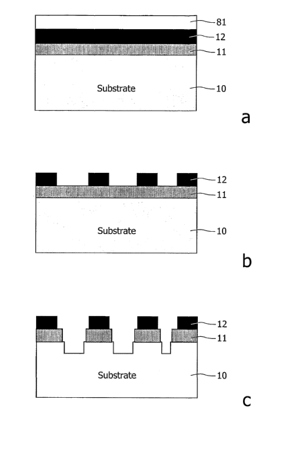
It is possible to use the patterned mask layer with relief structure as a mask
layer for further development of the underlying layer. Further development
means the further
selectively removal of material from the master substrate, in particular from
the interface
layer, for obtaining a deeper relief structure. This process is schematically
shown in Figure
13. The upper figure (figure 13a) shows the master substrate with protection
layer (81), mask
layer (12), interface layer (11), metal layer (83) and substrate (10). After
illumination and
developing (patterning) of the mask layer (12), the result given in figure
13b, the etching
liquid can come in contact with the interface layer (11) as well. Selective
exposure of the
interface layer to the etching fluid will cause that the relief structure
embedded in the mask
layer is further transferred into the interface layer (11). This is
schematically shown in figure
13c. The great advantage of this embodiment is to obtain deep relief
structures. The etching
liquid used for etching the interface layer may be of a different type than
that used to pattern
the mask layer.
In case no metallic layer (83) is used, the relief structure can be further
etched
into the substrate to obtain a further deepening of the relief structure. This
process is
schematically shown in Figure 14. The master substrate comprises a protection
layer (81), a
mask layer (12), an interface layer I1 and substrate (10). After illumination
and developing
(patterning) of the mask layer (12), the result given in figure 14b, the
etching liquid can come
in contact with the interface layer (11) as well. Selective exposure of the
interface layer to the
etching fluid will cause that the relief structure embedded in the mask layer
is further
transferred into the interface layer (11) and substrate (10). This is
schematically shown in
figure 14c. The great advantage of this embodiment is to obtain even deeper
relief structures.
2 5 It is also possible to use the patterned mask layer with relief structure
as a
mask layer for further illumination of the interface layer I1. The interface
layer I1 is, for
example, made of a photosensitive polymer. Illumination of the master
substrate with for
example W light will cause exposure of the areas which are not covered with
the mask
layer. The areas of the interface layer covered with the mask layer are not
exposed to the
3 O illumination since the mask layer is opaque for the used light. The
exposed interface layer I1
can be treated in a second development step, with a developing liquid not
necessarily be the
same as the liquid used to pattern the mask layer. In this way, the relief
structure present in
the mask layer is transferred to the interface layer Il such that a deeper
relief structure is
obtained.
CA 02562485 2006-10-11
WO 2005/101398 PCT/IB2005/051165
13
The proposed master substrate with protection layer is also perfectly suited
for
mastering with liquid immersion. Liquid immersion mastering is a mastering
concept to
increase the numerical aperture of the objective lens to above 1. Water is
present as an
intermediate medium in between the objective lens and the master substrate
instead of air.
Water has a higher index of refraction (n) than air. In the preferred
mastering method, a
temperature increase of at least 500-800 is required to induce melting of the
phase-change
layer. In particular in case a liquid film is present on top of the phase-
change layer, a
significant amount of heat will be lost through the liquid film. This heat
loss leads to:
1) a very higher laser power for recording data. In most laser beam recorders,
the
available laser power is limited. Therefore, a significant heat loss is not
permitted.
2) broadening of the thermal write spot. This is explained from the lateral
heat
spreading due to the presence of a good thermal conductor in the vicinity of
the mask layer.
The size of the focused laser spot is determined by the optics of the system.
This focused
laser spot causes laser-induced heating by the absorption of photons in the
recording stack. In
case a good thermal conductor is present in the vicinity of the mask layer,
lateral spreading
will cause a broadening of the temperature distribution. Since the proposed
method is based
on thermally induced phase transitions, this temperature broadening leads to
larger marks and
leads to a reduced data density.
The proposed protection layer acts as a good insulator, preventing the heat
loss
from the mask layer. In case such a protection layer is applied, the optical
spot resembles
almost the thermal spot such that small marks can be written. The thermal
conductivity of the
proposed organic protection layers is between 0.2 and 0.4 W/mK.
An additional advantage is the protection against water of the mask layer. The
protection layer can be seen as a seal during liquid immersion mastering.