Note: Descriptions are shown in the official language in which they were submitted.
CA 02562748 2006-10-13
WO 2005/103944 PCT/CA2005/000598
1
TITLE OF THE INVENTION
A nano molecular modeling method
FIELD OF THE INVENTION
[0001] The present invention relates to molecular modeling
in the nano scale. More specifically, the present invention is concerned
with a modeling method for nano systems.
BACKGROUND OF THE INVENTION
[0002] Electronic device modeling methods have allowed an
incredible development rate of microtechnology, by allowing engineers
to predict the performance of a technology emerging at the time. ,
[0003] Similarly, nano-tech modeling methods would allow
developing nano-electronics and nanotechnology to a full potential by
enabling rapid design and validation of nano-scale materials and
devices. Such nano-tech modeling methods for electronic device
properties do not yet exist today for lack of proper theoretical formalism
and of associated modeling tool.
[0004] As people in the art are well aware of, the properties
of electronic systems at a nano-meter scale are strongly influenced by
CA 02562748 2006-10-13
WO 2005/103944 PCT/CA2005/000598
2
quantum mechanical effects, and derive from conceptually different
device structures and operation principles. State-of the-art electronic
device modeling methods based on atomistic quantum mechanical first
principles can currently only deal with systems involving roughly 1000
atoms or less, due to theoretical and numerical complexities. This
severely limits their relevance for most large scale nanotechnology
systems.
[0005] A remarkable miniaturization of semiconductor micro-
electronics has been taking place over the past several decades. If the
miniaturization trend is to continue, devices are expected to reach a
physical limit in a near future (see The International Technology
Roadmap for Semiconductors, Technical Report, Semiconductor
Industry Association, San Jose, CA (2003)). At that time, electronic
devices will no longer work under designs as currently known, and will
require an understanding of conceptually different device structures
and operation principles.
[0006] Therefore, a challenge in the field of nanoelectronics
is to develop adequate modeling methods.
[0007] As it stands now, efforts in the field of nanoelectronics
have been conducted in at least two distinct domains. On the one hand,
an "up-to-bottom" approach of microtechnology applies the scaling
down of semiconductor microtechnology to the device feature size
CA 02562748 2006-10-13
WO 2005/103944 PCT/CA2005/000598
3
regime of below 50nm. Quantum effects are expected to play a very
important role for the operation of such ultra-small semiconductor
devices. On the other hand', there has been the advent of "bottom-to-
up" fabrication of devices from assembling individual molecules and
groups of atoms at a length scale of about 1 nm, in which quantum
effects not only play an important role, but also provide some of the
basic device principles. The latter efforts tend to a scaling up of sub-
nanometer scale devices such as single molecule devices and nano-
electromechanic systems (known as. NEMS).
[0008] Importantly, a present trend seems to indicate that
these efforst are leading to a near future where nanoelectronics are
expected to operate, hence a need for a molecular modeling methods
to understand how such nanoelectronic devices work.
[0009] Although the modeling of semiconductor technology
has a long history, its basic physical principle lies in classical or semi-
classical physics, where quantum effects and atomistic details of the
devices are largely ignored. Such modeling is heavily dependent on
material and electronic parameters obtained by fitting to experimental
data, which is becoming increasingly expensive and less reliable as
device size continues to shrink. Furthermore, due to fundamental
limitations, traditional microelectronic devices theory and modeling
methods are insufficient and even invalid when quantum effects are
CA 02562748 2006-10-13
WO 2005/103944 PCT/CA2005/000598
4
involved, for example in the case of charge transport at the up-coming
scale between 30 nm and 50 nm.
[0010] For full quantum mechanical first principles atomistic
analysis of materials and electronics, a most widely used and most
powerful formalism is the density functional theory (known as DFT).
Since DFT is able to solve quantum mechanic model including all
atomic details, it has been applied to many different problems to predict
structural and mechanical properties of materials, optical and electronic
properties of matter, molecular modeling in chemistry, biological and
drug-design applications, etc. The success of DFT is evidenced by the
Nobel Prize awarded to its original discoverer, Prof. Walter Kohn, in
1998. However DFT methods of analysis of materials property has so
far been applied to systems involving, in most cases, from a few tens to
a few hundred atoms due to the complexity of the theory and its time
consuming numerical procedure. In 'other words, at present, quantum
mechanical atomistic analysis methods are limited to systems with a
linear size less than about 5 nm.
[0011] At a technical level, a typical nano-electronic device
can be considered as comprising a device scattering region, such as
the channel region of a Si transistor, a large molecule, or a collection of
atoms for example, contacted by a number of long and different
electrodes where bias voltages are applied and electric current
collected. There can be a number of gates with gate voltages
CA 02562748 2006-10-13
WO 2005/103944 PCT/CA2005/000598
modulating the current flow. The typical nano-electronic device is
further interacting with an environment such as a substrate or other
devices nearby.
[0012] To deal with such a typical nano-electronic device, a
5 most realistic approach is clearly based on DFT, which has a potential
to handle large systems and includes most of the important microscopic
physics. However, DFT methods are so far largely limited to two
classes of problems at equilibrium, namely electronic states of finite
system such as an isolated molecule, and electronic states of periodic
system consisting of repeated units.
[0013] The typical nano-electronic device, however, is
neither finite nor periodic, and is typically operating under non-
equilibrium conditions. First, it is not finite since it is connected to a
number of electrodes and interacts with an environment involving a
practically infinite number of atoms. Second, it is not periodic since it
does not have translational symmetry. Third, it is away from equilibrium
since external bias voltages are applied to drive a current flow. These
features of the typical nano-electronic device need be resolved with a
nano-modeling method.
[0014] To date, there have been a few theoretical attempts
for analyzing quantum transport of devices at a truly molecular scale
using DFT (see for example: N.D. Lang, Phys. Rev. B, 52, 5335,
CA 02562748 2006-10-13
WO 2005/103944 PCT/CA2005/000598
6
(1995); K. Hirose, M. Tsukada, Phys. Rev. B 51, 5278 (1995); C.C.
Wan, J. L. Mozos, G. Taraschi, J. Wang and H. Guo, Appl. Phys. Lett.,
71, 419, (1997); H. J. Choi and J. Ihm, Phys. Rev. B, 59, 2267, (1999);
J. Taylor, H. Guo and J. Wang, Phys. Rev. B 63 245407 (2001 ); J.
Taylor, Ph. D. thesis, McGill University (2000); M. Brandbyge, J. L.
Mozos, P. Ordejdn, J. Taylor and K. Stokbro, Phys. Rev. B 65 165401
(2002)).
[0015] Although fully recognizing the important contributions
of these works to molecular electronics theory, it is however noted that
~10 they have a number of fundamental limitations. For example, methods
based on periodic boundary condition cannot deal with open device
structures, and methods based on the jellium model for device
electrodes (rather than realistic atomic electrodes) are too crude to deal
with device-electrode contacts. In addition, most existing methods can
only treat a number of atoms less than a few hundred and are very
difficult, if applicable at all, to extend to much larger scale.
[0016] At present, the most promising atomistic modeling
methods in the nano-range are based on carrying out DFT analysis
within the Keldysh non-equilibrium Green's function (NEGF) formalism.
This technique, as first developed by the present inventors, allows
parameter-free analysis of devices involving as large as about 1000
atoms in the device channel region (see J. Taylor, H. Guo and J. Wang,
Phys. Rev. B 63 245407 (2001 )J. Taylor, Ph. D. thesis, McGill
CA 02562748 2006-10-13
WO 2005/103944 PCT/CA2005/000598
7
University (2000); H. Mehrez, Ph. D. thesis, McGill University (2001);
B. Larade, Ph. D. thesis, McGill University (2002); P. Pomorski, Ph. D.
thesis, McGill University (2002); P. Pomorski, C. Roland, H. Guo and J.
Wang, Phys. Rev. B 70, 115408 (2004); P. Pomorski, Phys. Rev. B 67,
161404 (2003); P. Pomorski, L. Pastewka, C. Roland, H. Guo and J.
Wang, Phys. Rev. B 69, 115418 (2004)).
[0017] Using a NEGF-DFT method they have developed, the
present inventors have so far investigated a number of important issues
of nano-electronics, including the quantitative comparison and
agreement with experimental data on transport properties of molecular
(C.- C. Kaun, B. Larade and H. Guo, Phys. Rev. B 67, Rapid
Communication, 121411 (2003), C. C. ICaun and Hong Guo, Nano
Letters, 3, 1521 (2003)), metallic (see H. Mehrez, A. Wlasenko, B.
Larade, J. Taylor, P. Grutter, and H. Guo, Phys. Rev. B, 65, 195419
(2002)), and Carbon nanowires (see B. Larade, J. Taylor, H. Mehrez,
and H. Guo, Phys. Rev. B, 64, 75420 (2001)); the understanding of
electronic levels of molecular devices (see B. Larade, J. Taylor, Q. R.
Zheng, H. Mehrez, P. Pomorski and H. Guo, Phys. Rev. B, 64, 195402
(2001 )); current triggered vibrational excitations in molecular transistors
(see S. Alavi, B. Larade, J. Taylor, H. Guo and T. Seideman, special
issue of Molecular electronics in Chemical Physics, 281, 293 (2002));
Carbon nanotubes (see J. Taylor, H. Guo and J. Wang, Phys. Rev. B
63 245407 (2001); J. Taylor, Ph. D. thesis, McGill University (2000); C.
-C. ICaun, B. Larade, H. Mehrez, J. Taylor, and H. Guo , Phys. Rev. B
CA 02562748 2006-10-13
WO 2005/103944 PCT/CA2005/000598
65, 205416 (2002)); fullerene tunnel junctions (see C. Roland, B.
Larade, J. Taylor, and H. Guo, Physical Review B, 65, Rapid
Communication, 8041401 (2002); J. Taylor, H. Guo and J. Wang,
Phys. Rev. B 63, Rapid Communication, 121104 (2001)); and non-
equilibrium charge distribution and nanoscale capacitors (see P.
Pomorski, C. Roland, H. Guo and J. Wang, Phys. Rev. B 67, 161404
(2003)). These and a number of other investigations of the present
inventors have established a basic working formalism for predicting
nano-electronics operation from quantum principle at devices length
scales of about 5 nm.
[0018] Still, a most important and urgent task in nano-
electronic device theory is to develop a theoretical formalism and an
associated modeling method, based on atomistic quantum mechanical
principles, which are powerful and accurate enough to analyze and
predict material and device properties from about 1 nm molecular
electronics all the way to about 50 nm semiconductor technology. This
means a first principles method that allows accurate quantum analysis
involving from one to about one million atoms.
[0019] Therefore there is a need for a molecular modeling
method for nanoscale systems.
CA 02562748 2006-10-13
WO 2005/103944 PCT/CA2005/000598
9
SUMMARY OF THE INVENTION
[0020] More specifically, there is provided a method for
modeling a system including a group of atoms and an open
environment comprising other atoms, the group of atoms interacting
with the open environment, whereby the group of atoms and an
interaction thereof with the open environment. are defined by
Hamiltonian matrices and overlap matrices, matrix elements of the
matrices being obtained by a tight-binding (TB) fitting of system
parameters to a first principles atomistic model based on density
functional theory (DFT) with a non-equilibrium density distribution.
[0021] Other objects, advantages and features of the
present invention will become more apparent upon reading of the
following non-restrictive description of embodiments thereof, given by
way of example only. ~ a
BRIEF DESCRIPTION OF THE DRAWINGS
[0022] In the appended drawings:
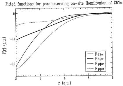
[0023] Figure 1 is a plot of fitted functions for parameterizing
on-site Hamiltonian of CNTs (Carbon Nanotubes), according to the
present invention;
a
CA 02562748 2006-10-13
WO 2005/103944 PCT/CA2005/000598
[0024] Figure 2 is a plot of fitted functions for parameterizing
two-wall carbon nanotube intra-shell off-site Hamiltonian according to
the present invention, as compared with ab initio results Hamiltonian;
[0025] Figure 3 is a plot of fitted functions for parameterizing
5 Carbon nanotube inter-shell Hamiltonian according to the present
invention, as compared with ab initio results Hamiltonian;
[0026] Figure 4 shows the transmission coefficient T(E) as a
function of energy E for a (5,5) carbon nanotube, obtained by ab initio
Hamiltonian (solid black line) and obtained by parameterized TB
10 Hamiltonian (dashed red line); and
[0027] Figure 5 shows I-V curves for a (5,5) carbon
nanotube obtained from the transmission T shown in Figure 4.
DESCRIPTION OF EMBODIMENTS OF THE INVENTION
[0028] There is provided a multi-scale modeling method,
which bridges a length scale gap between the two domains of current
nano-systems discussed above, and therefore provides a powerful
means to help developing a future generation of electronic devices, and
has a wide range of applicability in the understanding and prediction of
material; electronic and transport properties of nanoscale systems.
CA 02562748 2006-10-13
WO 2005/103944 PCT/CA2005/000598
11
[0029] Based on previous methods developed so far as
described hereinabove, the present method allows a qualitative leap,
whereby nanosystems comprising from a single atom all the way to
about 50 nm may be modeled.
[0030] The present method for bridging length scales in
nano-electronics modeling has been developed along four directions,
as follows: for devices involving up to about a few thousands atoms,
even up to 10,000 atoms, the method comprises using a self-consistent
first principles atomistic formalism; for devices involving up-to one
million atoms, the method comprises using a tight binding atomistic
formalism; the method is developed for a wide range of application
formalisms for nano-electronics device modeling; and the method
comprises using powerful computer cluster system for parallel
computation.
[0031] A nano-electronic device as referred to herein is a
system including a group of atoms (referred to as the device-group')
interacting with an open environment (referred to as the environmental-
group) comprising other atoms or/and a continuum of material. The
system is specified by a three-dimensional structure of atoms, including
their positions and types, in a device scattering region thereof, and
electrodes. Mathematically, this system .is defined by a Hamiltonian
operator H, which includes electron-electron and electron-ion
interactions, the environmental-group and external forces, so that once
CA 02562748 2006-10-13
WO 2005/103944 PCT/CA2005/000598
12
this Hamiltonian operator H is known all system properties may be
deduced.
[0032] For devices involving up to a few thousands atoms,
the method comprises using a self-consistent first principles atomistic
formalism. More specifically, the method uses a DFT atomistic
approach to predict device properties fully self-consistently without
resorting to any phenomenological parameter, as described elsewhere
by the present inventors (see J. Taylor, H. Guo and J. Wang, Phys.
Rev. B 63 245407 (2001); J. Taylor, Ph. D. thesis, McGill University
(2000); H. Mehrez, Ph. D, thesis, McGill University (2001 ); B. Larade,
Ph. D. thesis, McGill University (2002); P. Pomorski, Ph. D. thesis,
McGill University (2002)).
[0033] In DFT, as described in the art (See, for example,
Density-Functional Theory of Atoms and Molecules, R.G. Parr and W.
Yang, (Oxford University Press, New York, 1989)), the Hamiltonian
operator H of the system is determined as a functional of a local
electron charge density p(r), i.e. H = H [p (r)~. In a transport problem,
the system has open boundaries connecting to electrodes and operates
under external bias and gate potentials, which drive the device to non-
equilibrium, i. e. the environmental-group comprises one or more
electrodes and possibly metallic gates and substrates where the device
is embedded, and the device-group is the electronic device scattering
region, which comprises at least one atom. The charge density p(r) is
CA 02562748 2006-10-13
WO 2005/103944 PCT/CA2005/000598
13
thus to be determined under such conditions. Obtaining Fi and p (r) is a
self-consistent process, wherein H is obtained from p (r), and then,
using H, p (r) is evaluated, in an iterative process until H converges. As
shown before by the present inventors, the device conditions may be
accounted for by using the Keldysh non-equilibrium Green's function
(NEGF) for example, to construct p (r) from Fi (J. Taylor, H. Guo and J.
Wang, Phys. Rev. B 63 245407 (2001 ); J. Taylor, Ph. D. thesis, McGill
University (2000); H. Mehrez, Ph. D. thesis, McGill University (2001); B.
Larade, Ph.. D. thesis, McGill University (2002); P. Pomorski, Ph. D.
thesis, McGill University (2002)).
[0034] The details of this NEGF-DFT formalism is rather
technical and only its main advantages over other known formalisms
will be briefly summarized herein for concision purpose, as follows:
(i) NEGF-DFT allows calculating the charge density p(r) for open
quantum systems under a bias voltage entirely self-consistently
without resorting to phenomenological parameters;
(ii) since p(r) is constructed from NEGF, the non-equilibrium nature
of device operation is handled properly;
CA 02562748 2006-10-13
WO 2005/103944 PCT/CA2005/000598
14
(iii) NEGF-DFT treats atoms in the device scattering region and in
the electrodes at equal-footing, therefore allowing realistic
electrodes and contacts modeling;
(iv) NEGF treats discrete and continuum parts of electron spectra at
equal footing, so that all electronic states are included properly
into the calculation of Fi.
[0035] It is to be noted that NEGF-DFT has already been
applied to devices with sizes and complexities no other atomistic
formalism of the art could handle.
[0036] In the present method, the NEGF-DFT formalism is
used to allow modeling of systems involving a large number of atoms,
based on the fact that the calculation cost of the system Hamiltonian Fi
scales as O (N), which means that the cost scales linearly with the
atomic degrees of freedom (N) inside the device scattering region.
[0037] More precisely, it was shown that a main
computational bottleneck of NEGF-DFT method is the calculation and
inversion of a large matrix {Hu,,) in order to calculate the NEGF, which is
needed in constructing the charge density. For example, considering
nine orbitals (s, p, d orbitals) per atom, in the case of 10, 000 atoms,
this matrix is 90, 000 x 90, 000, and it is prohibitively time consuming to
CA 02562748 2006-10-13
WO 2005/103944 PCT/CA2005/000598
invert such a large matrix tens of times during the DFT. iteration.
However, it is noted that the atomic orbitals decay rapidly to zero from
the atomic core, which results in that distant atoms do not have a direct
orbital overlap. Furthermore, it has been shown that it is possible to "cut
5 ~ ofF' the orbital tails at some cut-off distance about several Angstroms
while still maintaining high accuracy (P. Ordejdn, E. Artacho and Josh
M. Soler, Phys. Rev. B. 53, 810441 (1996)).
[0038] Hence, due to the finite ranginess of the atomic basis,
a matrix element H~,, is zero if atoms p and v are located further than
10 twice the cut-off distance: Using this fact, the present method
comprises cutting the device scattering region into a number of sub-.
boxes each having a linear size , at least equal to twice the cut-off
distance. As a result, atoms in each sub-box only "interact" with other
atoms in the same sub-box and in nearest-neighbor sub-boxes. The
15 resulting matrix {H,~"~ is then block-tridiagonal and may be inverted
within O (N2) operations (instead of O (N3) for dense matrices).
[0039] In addition, to calculate charge density from non-
equilibrium Green's functions, only a very small portion of the NEGF
matrix, which is related to the inverted ~H~,,~, is needed, and the
calculation of NEGF is further reduced to O (N) operations because
most of its elements do not need to be calculated. Indeed, technically,
NEGF is calculated from the Keldysh equation G' = Gr E' Ga, where
G~'a are retarded and advance Green's functions obtained by inverting
CA 02562748 2006-10-13
WO 2005/103944 PCT/CA2005/000598
16
the {H,~,,] matrix. The matrix ~', referred to as the self-energy, describes
charge injection from the electrodes, and couples the scattering region
to the electrodes. Most matrix elements of ~' are zero, except those
corresponding to electrode atoms in the immediate neighboring sub-
s boxes to the scattering region. Because of this form of the self-energy
~', only a part of the Green's functions G~'a needs to be calculated in
order to obtain the NEGF G'. Therefore, due to this O (N) nature, the
matrix to be inverted in computing NEGF is not the full 90, 000 x 90,
000, matrix (in the above example of 10,000 atoms), but reduces to a
number of sub-matrices with a size corresponding to the orbitals in sub-
boxes. The size of these sub-matrices is estimated to be about 3, 000 x
3, 000 'using a typical value of orbital cut-off (as assessed for example
in P. Ordejdn, E. Artacho and Josh M. Soler, Phys. Rev. B. 53, 810441
(1996)) between about 5 - 6 A, and this sub-matrix size does not
increase when the total number of atoms increases. As people in the
art will appreciate, a matrix of such .size is easily inverted, and inversion
of a number of them is highly parallelizable.
[0040] Therefore, the present method allows handling
systems as large as a few thousands atoms totally self-consistently.
[0041] For devices involving up-to one million atoms, the
present method further comprises using a tight binding atomistic
formalism to model the about 50 nm nano-electronic devices, where a
very large number of atoms is involved. Although this scale is too large
CA 02562748 2006-10-13
WO 2005/103944 PCT/CA2005/000598
17
for the NEGF-DFT method even considering the development
described hereinabove, it may be handled by the present method by
using a parameterized tight-binding (TB) model in which a device
Hamiltonian HTB is parameterized instead of being dynamically
calculated. For device modeling, HTB is to reflect the presence of
external fields driving the current flow, and other open environmental
effects such as the charge transfer from the electrodes during
transport, which existing TB methods in the art do not allow. Therefore
existing TB methods appear unsatisfactory for nano-electronics
modeling.
[0042 The present method makes use of the NEGF-DFT
method developed by the present inventors and described hereinabove
to calculate Hamiltonian matrix ~H,~,,~ on devices with a smaller number
of atoms, as a function of external bias and gate fields. The resulting
~H~,,} is then fitted into a TB form {HTB ~. The resulting ~HTa } thus
~v
obtained includes all the effects of the device environment, and
therefore reproduces, to a large extent, the full self-consistent transport
results of the original device model {I=fu,,j~.
[0043 For much lager systems, {H~~j~ is used to calculate
transport directly, which saves the time consuming self-consistent DFT
CA 02562748 2006-10-13
WO 2005/103944 PCT/CA2005/000598
18
iteration of computing ~H,~,,). Cases with carbon devices were
successful.
(0044] A number of ways are contemplated in order to
determine an optimized strategy for parameterizing HTB to reflect the
device operation environment. As will be further described hereinafter,
these ways include for example directly using bias and gate voltages as
fitting parameters; parameterizing using average electric field strength
inside the scattering region; and parameterizing using local orbital
charge densities.
(0045] For non-equilibrium charge and spin transport, the
fitting of TB parameters is done by fitting to the Hamiltonian matrix
elements obtained from the ab initio NEGF-DFT method, described
above. Examples of the fitted parameters are in Figures 1-3.
(0046] The fitting of the TB parameters may further be
facilitated by fitting to the electron transmission coefficient T (E, Vb, V9),
which is obtained from the first principles DFT methods, and which is a
function of electron energy E, external bias voltage Vb, and external
gate voltage V9. The transmission coefficient T (E, Vb, V9) describes the
probability for an electron to traverse the device-group from one part of
the environmental-group (an electrode) to another part of the
environmental-group (a second electrode).
CA 02562748 2006-10-13
WO 2005/103944 PCT/CA2005/000598
19
[0047] This fitting of the TB parameters may further be
facilitated by further fitting to a bias dependent density of states, DOS
(E, Vb, V9), calculated from first principles, and by further fitting to
equilibrium properties of the device system (at zero bias potentials).
Furthermore, it may be contemplated fitting to charge and spin current,
the non-equilibrium charge distribution that is established during current
flow, the quantum mechanical forces with and without external bias and
gate voltages.
[0048] The transmission coefficient T (E, Vb, Vg) used to fit
the TB parameters is obtained from a first principles quantum
mechanical calculation, and fitting to T (E, Vb, V9) comprises performing
first principles quantum mechanical calculations on the device system
to obtain T (E, Vb, Vg) and other equilibrium properties; performing TB
~ calculations on the same system to obtain approximate transmission
coefficient TTB (E, Vb, V9) and approximate equilibrium properties; and
minimizing the difference between T (E, Vb, Vg) and TTB (E, Vb, Vg), as
well as between the equilibrium properties, by adjusting the TB
parameters for all applied voltages.
[0049] A similar fitting procedure applies for fitting to other
properties.
[0050] From the foregoing, it appears that the full self-
consistent NEGF-DFT method of the nano-modeling as described
CA 02562748 2006-10-13
WO 2005/103944 PCT/CA2005/000598
hereinabove can be used to generate TB parameters which depend on
external fields, thereby allowing nano-electronics modeling involving a
very large number of atoms. As a result, the method may allow
modeling devices involving one million atoms.
5 [0051] The application possibility of the present nano-
modeling method is extremely wide ranged. It may be applied for
example to the following:
(i) The investigation of nanotube field effect devices on
semiconductor substrate, as experimentally fabricated (see
10 details of fabrication in J. Appenzeller, J. Knoch, V. Derycke,
R. Martel, S. Wind, and Ph. Avouris, Phys. Rev. Lett. 89,
126801 (2002)). Nano-electronic devices on realistic
substrates have never been investigated theoretically to any
satisfaction due to the large number of atoms involved, but
15 may be within reach with the present nano-modeling method.
(ii) Study of electric conduction in self-assembled monolayer
(SAM) systems. SAM is a very important system and exactly
how charge flows through a SAM must now be understood.
(iii) Investigation of Si devices at a scale of 10 to 50 nm channel
20 length. Leakage current of ultra-thin oxides may also be
calculated. It is also possible to investigate other nano-meter
CA 02562748 2006-10-13
WO 2005/103944 PCT/CA2005/000598
21
scale semiconductor devices made by compound
semiconductors.
(iv) The study of AC transport properties of nano-electronics. As .
discussed elsewhere before by the present inventors, new
physics arise in AC transport at nanoscale due to induction,
which becomes much, stronger for systems with a reduced
density of states (see B. G. Wang, J. Wang and H. Guo,
Phys. Rev. Lett, 82, 398 (1999); C. Roland, M. B. Nardelli, J.
Wang and H. Guo, Phys. Rev. Lett. 84, 2921 (2000)).
(v) Modeling of transport properties of hybrid devices including
normal-superconductor, normal-magnetics, and normal-
biomolecular hybrids: superconductor and magnetic materials
contribute more complicated self-energies to the NEGF, but
relevant formulas have already been derived for these
systems (see H. Mehrez, J. Taylor, H. Guo, J. Wang and C.
Roland, Phys. Rev. Lett., 84, 2682 (2000); Q. F. Sun, H. Guo,
and T. H. Lin, Phys. Rev. Lett. 87, 176601 (2001 ); Y. Wei, J.
Wang, H. Guo, H. Mehrez and C. Roland, Phys. Rev. B. 63,
195412 (2001 ); N. Sergueev, Q. -F. Sun, H. Guo, B. G. Wang
and J. Wang, Phys. Rev. B 65, 165303 (2002)), and are
ready to be implemented into the present nano-modeling
method.
CA 02562748 2006-10-13
WO 2005/103944 PCT/CA2005/000598
22
(vi) Charge conduction in bio-molecules may be investigated.
Bio-molecules such as DNA may be used to build nanoscale
networks of conductors, they may also conduct charge
themselves. These properties are strongly influenced by
environmental effects such as the presence of water
molecules and their study involves a large number of atoms.
(vii) Current induced structural changes may be studied. The
present method allows the calculation of current-induced
quantum mechanical forces, molecular vibrational spectrum
. during current flow, and other current triggered molecular
dynamics.
(viii) Calculation of switching speed of current in nanoscale
devices. When a voltage pulse is applied to a nanoelectronic
device, the current turns on and turns off' according to the
pulse duration. The present method allows the calculation of
this switching speed including all quantum contributions to
resistance, capacitance and inductance.
(ix) Investigation of how two or more nanoelectronic devices
couple and work in a circuit. Interaction between devices at
the nanoscale is a very important problem and may be solved
by the present method.
CA 02562748 2006-10-13
WO 2005/103944 PCT/CA2005/000598
23
(x) STM simulations: scanning tunneling microscopes (STM) are
commonly used in a wide range of fields by passing a current
through the subject of study into a substrate. The present
method may be used to predict and help explaining STM
images without resorting to approximations used in
conventional STM theory.
[0052] The present nano-modeling method may further be
applied to model the coupling strength between electrons and
molecular vibrations during current flow in a nanoscale device, as well
as the modeling of inelastic current and local heating properties of the
device.
[0053] Figures 1 to 5 present results obtained by the present
method, in modelling of various carbon nanotube systems (CTN).
[0054] Unlike prior art methods for obtaining tight-binding
parameters by fitting ab initio calculated electronic band structures
and/or total energies of various different atomic structures, the present
method provides a set of tightbinding-like parameters by directly
parameterizing ab initio calculated Hamiltonian matrix elements. On
various carbon nanotube systems, as show in Figures 1 to 5, the
obtained parameters reproduce the ab inifio Hamiltonian matrix
elements very precisely and are transferable within a class of atomic
structures with similar topological properties. The reliable parame-
CA 02562748 2006-10-13
WO 2005/103944 PCT/CA2005/000598
24
terized Hamiltonian then reproduces all transport results of the original
ab initio calculated Hamiltonian.
[0055] The procedures for obtaining the parameters as
plotted in Figures 1 to 5 is recalled below.
[0056] First, the Hamiltonian matrix ~Hu~} is obtained by the
NEGF-DFT method. For parameterization of this Hamiltonian, the on
site part, related to each single atom in the structure, i.e. the atomic
orbital index u, v of the on-site matrix ,elements {H,",} belonging to the
same atom; and the hopping part of the matrix elements, related to two
adjacent atoms, are dealt with separately, as follows:
[0057] (i) On-site part: for a carbon nanotube (CNT)
system, a spa basis set is used. By transforming each 4 x 4 on-site
submatrix of the Hamiltonian matrix ~H,",~ into its equivalent form
defined on local coordinates of each site, it is found that the energy
difference between p-orbitals perpendicular to and parallel to the CNT
surface is as large as 5 eV, indicating that a conventional tight-binding
scheme with a constant on-site p-orbital energy can not reproduce the
ab initio Hamiltonian {NN"}. In addition, it is found that the Hamiltonian
element between s-orbital and the p-orbital perpendicular to the CNT
surface is about 1 eV, in contrast the zero value adopted by the
conventional tight-binding scheme. Further calculation shows that both
the energy difference between p-orbitals and the small element
CA 02562748 2006-10-13
WO 2005/103944 PCT/CA2005/000598
between s-orbital and the p-orbital perpendicular to the CNT surface
affect transport results significantly, and that, therefore, they can not be
neglected. Based on the above analysis, the matrix element values of
the on-site part of ~HN"~ are decomposed into contributions from every
5 neighbor atoms of the site. In this way, environment effects on the site is
included and the matrix elements are parameterized very precisely with
a maximum error being within tens of meV. The decomposition is
performed around the Slater-Koster two-center approximation, which
was originally used in the conventional tight-binding scheme for the
10 hopping part of the Hamiltonian. With the Slates-Koster two-center
approximation, the 16 on-site elements of {NN"} for each site i are
written as follows:
Ess = E° + ~ F'ssa ~,~
O
Esa ~~a~~lj~~spa~J~
J~xi
i _ ~ ~(' ,+ ~~, ~ ~ ~
Eap-EaVap j~)~~a j"~ p ~"ij Fppa ij ~aep a ~Ij p ~tj 1' ppn ij
xi
where a, f3 are coordinates x, y, z; ES°and E«° are atomic
orbital
15 energies of corresponding isolated atom; and the functions FsSa, Fspa,
Fpp6 and Fpp.~ are determined numerically by fitting the ab initio on-site
elements of ~HN~} for a number of different CNT structures: Those fitted
functions FSSa, Fspa, Fppa and Fpp.~ are plotted as a function of distance r
in Figure 1.
CA 02562748 2006-10-13
WO 2005/103944 PCT/CA2005/000598
26
(ii) Hopping part: Similar to the analysis on the on-site part of
~H~,~), local coordinates are redefined for.each pair of atoms and then
the corresponding 4 x 4 hopping submatrix of {H,",~ is transformed into
its equivalent form defined on the redefined local coordinates. By
plotting all the matrix elements defined on the local coordinates against
distance between the pair of atoms, it is found that the elements
between p-orbitals perpendicular to the CNT surface and the elements
between p-orbitals parallel to the CNT surface fall on two distinctly
different curves. The energy difference of the two .curves, at the
distance between two nearest neighbor atoms, is as large as 1 eV,
which indicates again that the conventional tight-binding scheme with
no difference between p-orbitals can not reproduce the ab initio
Hamiltonian ~HN~~. It is found that ignoring the difference between the .
two curves and using average values thereof completely changes the
transport properties of the original ab initio Hamiltonian ~Hr,~~, which
means that for reproducing the transport properties the difference
between the two curves needs to be taken into account. Once the
difference between p-orbitals is thus taken into account, all matrix
elements of the hopping part of {Hug}, after being transformed to local
coordinates, is found either to be close to zero or to fall on six smooth
curves VSSa, Vspa, Vpsa, Vppa, Vpp~ ~~~ and Vpp.~ ~2~, which are then be
easily parameterized, with Vpsa = - Vspa. Figure 2 shows plots of VSS6,
VSp6, VpSa, Vpp6, Vpp,~ ~~~ and Vpp.~ ~~) as a function of distance r for
constructing two-wall carbon nanotube intra-shell off-site
CA 02562748 2006-10-13
WO 2005/103944 PCT/CA2005/000598
27
Hamiltonian, as compared with ab initio results, showing an
agreement between the TB method and the present NEGF-DFT
method.
(0058] In multi-shell systems, such as multi-wall CNTs, the
intershell interaction is different from intrashell interaction. With a
similar analysis as hereinabove, it is found that for intershell interaction,
there is no observable difference between Vpp.~ ~~) and Vpp.~ ~2~ as in the
case of intrashell interaction, and a single empirical curve describes the
pp~ interaction. Then, as shown in Figure 3, the intershell part of the
ab initio Hamiltonian matrix elements can be well reproduced by
smooth curves Vssa, Vsp~.,, VpSa, Vpp~., and Vpp~a as a function of distance
r.
Again, VpSa = - Vspa.
(0059] Figure 4 illustrates the transmission coefficient T(E)
as a function of energy E for a (5,5) carbon nanotube, obtained by ab
initio Hamiltonian (solid black line) and by parameterized TB
Hamiltonian (dashed red line). Almost perfect agreement is obtained.
(0060] Figure 5 illustrates I-V curves for a (5,5) carbon
nanotube obtained from the transmission T shown in Figure 4, showing
an almost perfect agreement between the TB and the ab initio
methods.
CA 02562748 2006-10-13
WO 2005/103944 PCT/CA2005/000598
28
(0061] A number of other systems may be studied, including
binary systems and alloys for example.
[0062] Generally stated, the present method, besides
allowing all molecular modeling as well as any existing methods, allows
modeling anything involving a current flow, including for example any
electronic devices modeling, structure changes due to current (NEMS),
sensors, storage device modeling, etc.
[0063] The present method further comprises using a
distributed computing strategy, for both NEGF-DFT and TB methods
discussed hereinabove, for parallel computation, allowed by the O (N)
nature previously described.
[0064] People in the art should now be in a position to
appreciate that, although the above description concentrated on
discussing charge transport, the scope of the present method clearly
goes way beyond this domain as it provides a completely new way to
carry out large scale atomistic analysis. It is believed the theoretical
and computational developments of this method will help to lay a solid
foundation to a general modeling strategy for nanotechnology.
[0065] People in the art will appreciate that the present
method, based on first principles quantum mechanical atomistic model,
for predicting electronic, transport, and materials properties of
CA 02562748 2006-10-13
WO 2005/103944 PCT/CA2005/000598
29
nanoscale devices, is unique in its theoretical formalism and its
modeling strategy. Importantly, the present method is capable of
handling much larger number of atoms than presently available
methods, and covers length scales from atomic level all the way to
about 50 nm. The present method has therefore a wide range of
application potential and unprecedented predictive power in the field of
nano-electronics and nanotechnology.
[0066] Although the present invention has been described
hereinabove by way of embodiments thereof, it may be modified,
without departing from the nature and teachings of the subject invention
as described herein.