Note: Descriptions are shown in the official language in which they were submitted.
CA 02563190 2011-09-01
CIRCUIT INTERRUPTING DEVICE WITH A SINGLE TEST-RESET BUTTON
BACKGROUND OF THE INVENTION
1. Field of the Invention
The present application is directed to a family of resettable circuit
interrupting
devices and systems that comprises ground fault circuit interrupters (GFCI's),
are fault
circuit interrupters (AFCI's), immersion detection circuit interrupters
(IDCI's), appliance
leakage circuit interrupters (ALCI's), equipment leakage circuit interrupters
(ELCI's),
circuit breakers, contactors, latching relays and solenoid mechanisms. More
particularly,
the present application is directed to circuit interrupting devices having a
single actuator
for breaking and making electrically conductive paths between a line side and
a load side
of the devices.
2. Description of the Related Art
Many electrical wiring devices have a line side, which is connectable to an
electrical power supply, and a load side, which is connectable to one or more
loads and
at least one conductive path between the line and load sides. Electrical
connections to
wires supplying electrical power or wires conducting electricity to the one or
more loads
are at line side and load side connections. The electrical wiring device
industry has
witnessed an increasing call for circuit breaking devices or systems which are
designed
to interrupt power to various loads, such as household appliances, consumer
electrical
products and branch circuits. In particular, electrical codes require
electrical circuits in
home bathrooms and kitchens to be equipped with ground fault circuit
interrupters
(GFCI), for example. A more detailed description of a GFCI device is provided
in U.S.
Pat. No. 4,595,894, which is incorporated herein in its entirety by reference.
Presently
available GFCI devices, such as the device described in commonly owned U.S.
Pat. No.
4,595,894 (the '894 patent), use an electrically activated trip mechanism to
mechanically
break an electrical connection between the line side and the load side. Such
devices are
resettable after they are tripped by, for example, the detection of a ground
fault. In
1
CA 02563190 2006-10-06
WO 2005/099393 PCT/US2005/011737
the device discussed in the '894 patent, the trip mechanism used to cause the
mechanical
breaking of the circuit (i.e., the conductive path between the line and load
sides) includes a
solenoid (or trip coil). A test button is used to test the trip mechanism and
circuitry used to
sense faults, and a reset button is used to reset the electrical connection
between line and load
sides.
However, instances may arise where an abnormal condition, caused by for
example a
lightning strike, occurs which may result not only in a surge of electricity
at the device and a
tripping of the device but also a disabling of the trip mechanism used to
cause the mechanical
breaking of the circuit. This may occur without the knowledge of the user.
Under such
circumstances an unknowing user, faced with a GFCI which has tripped, may
press the reset
button which, in turn, will cause the device with an inoperative trip
mechanism to be reset
without the ground fault protection available.
Further, an open neutral condition, which is defined in Underwriters
Laboratories (UL)
Standard PAG 943A, may exist with the electrical wires supplying electrical
power to such
GFCI devices. If an open neutral condition exists with the neutral wire on the
line (versus
load) side of the GFCI device, an instance may arise where a current path is
created from the
phase (or hot) wire supplying power to the GFCI device through the load side
of the device
and a person to ground. In the event that an open neutral condition exists,
current GFCI
devices, which have tripped, may be reset even though the open neutral
condition may remain.
Commonly owned U.S. Patent 6,040,967 having Serial No. 09/138,955, which is
incorporated herein in its entirety by reference, describes a family of
resettable circuit
interrupting devices capable of locking out the reset portion of the device if
the circuit
interrupting portion is non-operational or if an open neutral condition
exists.
Some of the circuit interrupting devices described above have a user
accessible load
side connection in addition to the line and load side connections. The user
accessible load side
connection includes one or more connection points where a user can externally
connect to the
electrical power supplied from the line side. The load side connection and
user accessible load
side connection are typically electrically connected together. An example of
such a circuit
interrupting device is a GFCI receptacle, where the line and load side
connections are binding
screws and the user accessible load side connection is a typical two or three
hole receptacle
2
CA 02563190 2006-10-06
WO 2005/099393 PCT/US2005/011737
used in power outlets for connection to electrical devices typically using a
three-prong or two-
prong male plug. As noted, such devices are connected to external wiring so
that line wires
are connected to the line side connection and load side wires are connected to
the load side
connection.
However, instances may occur where the circuit interrupting device is
improperly
connected to the external wires so that the load wires are connected to the
line side connection
and the line wires are connected to the load connection. This is known as
reverse wiring. In
the event the circuit interrupting device is reverse wired, fault protection
to the user accessible
load connection may be eliminated, even if fault protection to the load side
connection
remains. Further, because fault protection is eliminated the user accessible
terminals (i.e.,
three hole or two hole receptacles) will have electrical power making a user
think that the
device is operating properly when in fact it is not. Therefore, there exists a
need to detect
faults when the circuit interrupting device is reverse wired. Also, there
exists a need to
prevent a device from being reverse wired. Further, there exists a need to
prevent the user
accessible load terminals from having electrical power when the circuit
interrupting device is
reverse wired or when the circuit interrupting device is not operating
properly.
Furthermore, some of the circuit interrupting devices described above include
two
buttons on the face of the device: a reset button and a test button. When the
device is in a
tripped condition, the user can depress the reset button to reestablish an
electrical connection
between the line and load connections, referred to as the reset state. When
the device is in the
reset state, the user can depress the test button to discontinue the
electrical connection between
the line and load connections, referred to as the tripped state.
3
CA 02563190 2006-10-06
WO 2005/099393 PCT/US2005/011737
SUMMARY OF THE INVENTION
The present invention relates to a family of resettable circuit interrupting
devices
having a single actuator for activating a circuit interrupting to break a
conductive path between
line side and load side of the device and using the same button for activating
a reset portion to
reestablish the conductive path. The devices prevent electric power from being
accessible to
users of such devices when these devices are reversed wired. The devices have
a reset lockout
mechanism that prevents them from being reset when they are not operating
properly. When
the devices are not reset and if such devices are reverse wired no power is
available to any user
accessible receptacles and/or plugs located on the face of the devices. Each
of the devices of
the present invention has at least one pair of line terminals, one pair of
load terminals and one
pair of face terminals. The line terminals are capable of being electrically
connected to a
source of power. The load terminals are capable of being electrically
connected to a load and
are improperly connected to electrical power when the device is reverse wired.
The face
terminals are electrically connected to user accessible plugs and/or
receptacles located on the
face of a device for example. The line, load and face terminals are
electrically isolated from
each other when the device is in its tripped condition. The devices of the
present invention are
manufactured and shipped in a trip condition, i.e., no electrical connection
between line
terminals and load terminals and no electrical connection between the load
terminals and face
terminals. Thus, in the trip condition the at least three terminals are
electrically isolated from
each other.
Each of the pairs of terminals has a phase terminals and a neutral terminal. A
phase
conducting path is created when the corresponding phase terminals are
connected to each
other. Similarly a neutral conducting path is created when the corresponding
neutral terminals
are connected to each other. Preferably, the phase conductive path includes
one or more
switch devices that are capable of opening to cause electrical discontinuity
in the phase
conductive path and capable of closing to reestablish the electrical
continuity in the phase
conductive paths. Also, the neutral conductive path includes one or more
switch devices that
4
CA 02563190 2006-10-06
WO 2005/099393 PCT/US2005/011737
are capable of opening to cause electrical discontinuity in the neutral
conductive path and
capable of closing to reestablish the electrical continuity in the neutral
conductive paths.
The devices of the present invention each further has a pair of movable
bridges which
are electrically connected to the line terminals. The movable bridges
electrically connect the
line terminals to the load and face terminals when the devices are reset thus
bringing power to
the face of the devices. The movable bridges are mechanically biased away from
the load and
face terminals. When the devices are improperly wired or reverse wired (i.e.,
power connected
to load terminals), the reset lockout mechanism prevents the movable bridges
from connecting
the line terminals to the load and face terminals even when an attempt is made
to reset the
device thus preventing electric power to be present at the face terminals or
user accessible
plugs and/or receptacles.
In one embodiment, the present application is directed to circuit interrupting
devices
that include a single test-reset button for triggering a reset portion and a
circuit interrupting
portion. The reset portion includes functionality to make electrically
conductive paths
between a line side and a load side of a device. The circuit interrupting
portion includes
functionality to break electrically conductive paths between the line side and
load side. In
particular, the circuit interrupting portion is an electro-mechanical
mechanism that comprises a
coil and plunger assembly, a latch plate and lifter assembly, a mechanical
switch assembly and
a mechanical trip actuator assembly. The circuit interrupting portion is
capable of
automatically tripping or breaking electrical connections between the load and
line side upon
detection of a fault or a predetermined condition. The circuit interrupting
portion also can
manually break electrical connections by using only the mechanical portion of
the circuit
interrupting portion using the test-reset button, the latch plate and lifter
assembly and the
mechanical trip actuator. The reset portion comprises common components as the
circuit
interrupting portion, particularly the same test-reset button. As a result,
the operation of the
device is simplified.
One embodiment for the circuit interrupting device uses an electro-mechanical
circuit
interrupting portion that causes electrical discontinuity between the line,
load and face
terminals. A reset lockout mechanism prevents the reestablishing of electrical
continuity
between the line, load and face terminals unless the circuit interrupting
portion is operating
5
CA 02563190 2006-10-06
WO 2005/099393 PCT/US2005/011737
properly. That is, the reset lockout prevents resetting of the device unless
the circuit
interrupting portion is operating properly. The reset portion allows the
device to be reset
causing electrical continuity between the line terminals and the load
terminals and electrical
continuity between the line terminals and the face terminals; i.e., device in
reset mode. Also,
there is electrical continuity between the load terminals and the face
terminals when the device
is reset. Thus the reset portion establishes electrical continuity between the
line, load and face
terminals. The electro-mechanical circuit interrupting portion comprises a
latch plate and
lifter assembly, a coil and plunger assembly, a mechanical switch assembly,
the movable
bridges, a mechanical trip actuator and the sensing circuit.
The reset condition is obtained by using the test-reset button. The test-reset
button is
mechanically biased and has a flange (e.g., circular flange or disk) that
extends radially from
an end portion of a pin for interference with the latch plate and lifter
assembly when the test-
reset button is depressed while the device is in the trip condition. The
interfered latch plate
and lifter assembly engages the mechanical switch assembly which triggers the
sensing circuit.
If the circuit interrupting portion is operating properly, the triggered
sensing circuit causes a
coil assembly coupled to the sensing circuitry to be energized. The energized
coil assembly,
which has a movable plunger located therein, causes a movable plunger to
engage the latch
plate to allow the end portion of the pin and the flange to go through
momentarily aligned
openings in the latch plate and lifter assembly. The openings then become
misaligned
trapping the flange and the end portion of the pin underneath the lifter. The
flange is now
positioned under the latch plate and lifter assembly. When the test-reset
button is released
after having been depressed, the biasing of the button is such that the pin
tends to move away
from the latch and lifter assembly. Upon release of the test-reset button, the
biasing of the pin
in concert with its interfering flange engages and lifts the latch plate and
lifter assembly.
Thus, the lifter engages the movable bridges to cause the bridges to
electrically connect the
line, load and face terminals to each other thus putting the device in a reset
condition. If the
circuit interrupting portion is not operating properly the plunger of the coil
assembly does not
engage the latch plate and lifter assembly thus preventing the circuit
interrupting device from
being reset.
6
CA 02563190 2006-10-06
WO 2005/099393 PCT/US2005/011737
The sensing circuit comprises various electrical and electronic components for
detecting the occurrence of a predetermined condition. The sensing circuitry
is coupled to the
electro-mechanical circuit interrupting portion. Upon detection of a
predetermined condition
the sensing circuitry activates the electro-mechanical circuit interrupter
causing the device to
be in the trip condition.
The trip condition can be obtained by activating the circuit interrupting
portion by
depressing the test-reset button when the device is in the reset state. The
trip condition can
also occur when the device detects a predetermined condition (e.g., ground
fault) while in the
reset mode. In one embodiment, when the test-reset button is depressed, while
the device is in
the reset mode, the test-reset button engages the mechanical trip actuator
causing a cam action
between the pin and the trip actuator resulting in the momentary alignment of
the lifter and
latch plate openings; this allows the end portion and flange of the pin to be
released from
underneath the lifter and thus no longer interfere with the lifter and latch
plate assembly. As a
result the lifter and latch plate no longer lift the movable bridges and the
biasing of the
movable bridges causes them to move away from the load and face terminals to
disconnect the
line, load and face terminals from each other thus putting the device in the
trip condition.
The foregoing has outlined, rather broadly, the preferred feature of the
present
invention so that those skilled in the art may better understand the detailed
description of the
invention that follows. Additional features of the invention will be described
hereinafter that
form the subject of the claims of the invention. Those skilled in the art
should appreciate that
they can readily use the disclosed conception and specific embodiment as a
basis for designing
or modifying other structures for carrying out the same purposes of the
present invention and
that such other structures do not depart from the spirit and scope of the
invention in its
broadest form.
7
CA 02563190 2006-10-06
WO 2005/099393 PCT/US2005/011737
BRIEF DESCRIPTION OF THE DRAWINGS
Other aspects, features and advantages of the present invention will become
more fully
apparent from the following detailed description, the appended claim, and the
accompanying
drawings in which similar elements are given similar reference numerals:
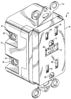
FIG. 1 is a perspective view of one embodiment of a ground fault circuit
interrupting
device according to the present application;
FIG. 2 is top view of a portion of the GFCI device shown in FIG. 1, with the
face
portion removed;
FIG. 3 is an exploded perspective view of the face terminal internal frames,
the load
terminals and the movable bridges;
FIG. 4 is a perspective view of the arrangement of some of the components of
the
circuit resetting and interrupting portion of the device of the present
invention;
FIG. 5 is a simplified side view of FIG. 4;
FIG. 6 is a schematic diagram of a sensing circuit of a GFCI;
FIGS. 7-10 show the sequence of operation when the device of the present
invention is
reset from a tripped state; and
FIGS. 11-12 show the sequence of operation when the device of the present
invention
is tripped from a reset state.
8
CA 02563190 2006-10-06
WO 2005/099393 PCT/US2005/011737
DETAILED DESCRIPTION
The present application contemplates various types of circuit interrupting
devices that
have at least one conductive path. The conductive path is typically divided
between a line side
that connects to electrical power, a load side that connects to one or more
loads and a user side
that connects to user accessible plugs or receptacles. As noted, the various
devices in the
family of resettable circuit interrupting devices comprise: ground fault
circuit interrupters
(GFCI's), arc fault circuit interrupters (AFCI's), immersion detection circuit
interrupters
(IDCI's), appliance leakage circuit interrupters (ALCI's) and equipment
leakage circuit
interrupters (ELCI's).
For the purpose of the present application, the structure or mechanisms used
in the
circuit interrupting devices, shown in the drawings and described hereinbelow,
are
incorporated into a GFCI device suitable for installation in a single-gang
junction box used in,
for example, a residential electrical wiring system. However, the mechanisms
according to the
present application can be included in any of the various devices in the
family of resettable
circuit interrupting devices. Further, more generally the circuit interrupting
device of the
present invention can be implemented as any device having at least a first,
second, and third
electrical conductor each of which is at least partially disposed in a
housing. The electrical
conductors are electrically isolated from each other with the first conductor
capable of being
connected to electrical power, the second conductor capable of being connected
to one or more
loads and the third conductor configured to be accessible to users. At least
one movable
bridge, one end of which is connected to the source of power and the first
conductor, is able to
connect the first, second and third electrical conductors to each other and
disconnect said
conductors from each other when a fault or predetermined condition is
detected.
More specifically, however, the circuit interrupting devices described herein
have at
least three pairs of electrically isolated terminals: at least one pair of
line terminals, at least
one pair of load terminals and at least one pair of user or face terminals.
The at least one pair
of line terminals permits electrical power (e.g., alternating current (AC)) to
be connected to the
device and the at least one pair of load terminals permits external conductors
or appliances to
be connected to the device. These connections may be, for example, electrical
fastening
9
CA 02563190 2006-10-06
WO 2005/099393 PCT/US2005/011737
devices that secure or connect external conductors to the circuit interrupting
device, as well as
conduct electricity. Examples of such connections include binding screws,
lugs, terminals and
external plug connections. The at least one face or user terminal, which
typically is
implemented using two-prong or three-prong receptacles, allows users to
electrically connect
electrical devices to the GFCI device typically via the two-prong or three-
prong male plugs
that mate with the receptacles.
The above-described features can be incorporated in any resettable circuit
interrupting
device, but for the sake of explanation the description to follow is directed
to a GFCI device.
In one embodiment, the GFCI device having a single test-reset actuator for
activating a
circuit interrupting or test portion to break a conductive path between line
side and load side
of the device and for activating a reset portion to reestablish the conductive
path. The reset
portion includes functionality to make electrically conductive paths between a
line side and a
load side of a device. The circuit interrupting portion includes functionality
to break
electrically conductive paths between the line side and load side. In
particular, the circuit
interrupting portion includes an electro-mechanical mechanism comprising a
coil and plunger
assembly, a latch plate and lifter assembly, a mechanical switch assembly and
a mechanical
trip actuator. The circuit interrupting portion is capable of automatically
tripping or breaking
electrical connections between the load and line side upon detection of a
fault or a
predetermined condition. The circuit interrupting portion also can manually
break electrical
connections by using only the mechanical portion of the circuit interrupting
portion
comprising the latch plate and lifter assembly and the mechanical trip
actuator. The reset
portion comprises the same components as the circuit interrupting portion,
particularly the
same test-reset button.
In another embodiment, the GFCI device has a circuit interrupting portion, a
reset
portion and a reset lockout mechanism. The GFCI device further has a pair of
movable
bridges that, when engaged, connect the line terminals to load and face
terminals. When the
bridge is not engaged, the line, load and face terminals are electrically
isolated from each
other. Because the face tenninals are electrically isolated from the load and
line terminals,
there will be no power at the face terminals even if the GFCI device is
reverse wired (power
connected to load terminals instead of line terminals). When the movable
bridge is not
CA 02563190 2006-10-06
WO 2005/099393 PCT/US2005/011737
engaged and thus the line, load and face terminals are electrically isolated
from each other, the
device is said to be in a tripped condition.
The circuit interrupting and reset portions described herein preferably use
electro-
mechanical components to break (open) and make (close) one or more conductive
paths
between the line and load terminals of the device and also between the line
and face terminals.
However, electrical components, such as solid state switches and supporting
circuitry, may be
used to open and close the conductive paths.
Generally, the circuit interrupting portion is used to automatically break
electrical
continuity in one or more conductive paths (i.e., open the conductive path)
between the line
and load terminals upon the detection of a fault, which in the embodiment
described is a
ground fault. Electrical continuity is also broken between the line and face
terminals. The
reset portion is used to close the open conductive paths.
In this configuration, the operation of the reset and reset lockout portions
is in
conjunction with the operation of the circuit interrupting portion, so that
electrical continuity
in open conductive paths cannot be reset if the circuit interrupting portion
is non-operational,
if an open neutral condition exists and/or if the device is reverse wired.
When the circuit
interrupting portion is non-operational---meaning that any one or more of its
components is
not operating properly---the device cannot be reset. The test-reset button is
able to break
electrical continuity between the line, load and face terminals independently
of the operation
of the circuit interrupting portion. Thus, in the event the circuit
interrupting portion is not
operating properly, the device can still be tripped.
Turning now to FIG. 1, the GFCI device 10 has a housing 12 to which a face or
cover
portion 36 is removably secured. The face portion 36 has entry ports 16, 18,
24 and 26 aligned
with receptacles for receiving normal or polarized prongs of a male plug of
the type normally
found at the end of a household device electrical cord (not shown), as well as
ground-prong-
receiving openings 17 and 25 to accommodate three-wire plugs. The GFCI device
also
includes a mounting strap 14 used to fasten the device to a junction box. A
single actuator
embodied as a test-reset button 20 forming a part of the reset portion extends
through opening
19 in the face portion 36 of the housing 12. The test-reset button 20
alternately activates both
a test operation (tripped condition) and reset operation (reset operation),
hence it is a dual
11
CA 02563190 2006-10-06
WO 2005/099393 PCT/US2005/011737
function button. The test-reset button 20 can be used to activate a reset
operation, which
reestablishes electrical continuity in the open conductive paths. The test-
reset button 20 also
can used to establish a trip condition by activating the circuit interrupting
portion of the
device. The circuit interrupting portion, to be described in more detail
below, is used to break
electrical continuity in one or more conductive paths between the line and
load side of the
device.
Still referring to FIG. 1, electrical connections to existing household
electrical wiring
are made via binding screws 28 and 30 where, for example, screw 30 is an input
(or line)
phase connection, and screw 28 is an output (or load) phase connection. Screws
28 and 30 are
fastened (via a threaded arrangement) to terminals 32 and 34 respectively.
However, the GFCI
device can be designed so that screw 30 can be an output phase connection and
screw 28 an
input phase or line connection. Terminals 32 and 34 are one half of terminal
pairs. Thus, two
additional binding screws and terminals (not shown) are located on the
opposite side of the
device 10. These additional binding screws provide line and load neutral
connections,
respectively. It should also be noted that the binding screws and terminals
are exemplary of
the types of wiring terminals that can be used to provide the electrical
connections. Examples
of other types of wiring terminals include set screws, pressure clamps,
pressure plates, push-in
type connections, pigtails and quick-connect tabs. The face terminals are
implemented as
receptacles configured to mate with male plugs. A detailed depiction of the
face terminals is
shown in FIG. 2.
Referring to FIG. 2, a top view of the GFCI device (without face portion 36
and strap
14) is shown. An internal housing structure 40 provides the platform on which
the
components of the GFCI device are positioned. Test-reset button 20 is mounted
on housing
structure 40. Housing structure 40 is mounted on printed circuit board 38. The
receptacle
aligned to opening 16 of face portion 36 is made from extensions 50A and 52A
of frame 48.
Frame 48 is made from an electricity conducting material from which the
receptacles aligned
with openings 16 and 24 are formed. The receptacle aligned with opening 24 of
face portion
36 is constructed from extensions 50B and 52B of frame 48. Also, frame 48 has
a flange the
end of which has electricity conducting contact 56 attached thereto. Frame 46
is an electricity
conducting material from which receptacles aligned with openings 18 and 26 are
formed. The
12
CA 02563190 2006-10-06
WO 2005/099393 PCT/US2005/011737
receptacle aligned with opening 18 of frame portion 36 is constructed with
frame extensions
42A and 44A. The receptacle aligned with opening 26 of face portion 36 is
constructed with
extensions 42B and 44B. Frame 46 has a flange the end of which has electricity
conducting
contact 60 attached thereto. Therefore, frames 46 and 48 form the face
terminals implemented
as receptacles aligned to openings 16, 18, 24 and 26 of face portion 36 of
GFCI 10 (see FIG.
1). Load terminal 32 and line terminal 34 are also mounted on internal housing
structure 40.
Load terminal 32 has an extension the end of which electricity conducting load
contact 58 is
attached. Similarly, load terminal 54 has an extension to which electricity
conducting contact
62 is attached. The line, load and face terminals are electrically isolated
from each other and
are electrically connected to each other by a pair of movable bridges. The
relationship
between the line, load and face terminals and how they are connected to each
other is shown in
FIG. 3.
Referring now to FIG. 3, there is shown the positioning of the face and load
terminals
with respect to each other and their interaction with the movable bridges (64,
66). Although
the line terminals are not shown, it is understood that they are electrically
connected to one
end of the movable bridges. The movable bridges (64, 66) are generally
electrical conductors
that are configured and positioned to connect at least the line terminals to
the load terminals.
In particular movable bridge 66 has bent portion 66B and connecting portion
66A. Bent
portion 66B is electrically connected to line terminal 34 (not shown).
Similarly, movable
bridge 64 has bent portion 64B and connecting portion 64A. Bent portion 64B is
electrically
connected to the other line terminal (not shown); the other line terminal
being located on the
side opposite that of line terminal 34. Connecting portion 66A of movable
bridge 66 has two
fingers each having a bridge contact (68, 70) attached to its end. Connecting
portion 64A of
movable bridge 64 also has two fingers each of which has a bridge contact (72,
74) attached to
its end. The bridge contacts (68, 70, 72 and 74) are made from relatively
highly conductive
material. Also, face terminal contacts 56 and 60 are made from relatively
highly conductive
material. Further, the load terminal contacts 58 and 62 are made from
relatively highly
conductive material. The movable bridges are preferably made from flexible
metal that can be
bent when subjected to mechanical forces. The connecting portions (64A, 66A)
of the
movable bridges are mechanically biased downward or in the general direction
shown by
13
CA 02563190 2006-10-06
WO 2005/099393 PCT/US2005/011737
arrow 67. When the GFCI device is reset the connecting portions of the movable
bridges are
caused to move in the direction shown by arrow 65 and engage the load and face
terminals
thus connecting the line, load and face terminals to each other. In particular
connecting
portion 66A of movable bridge 66 is bent upward (direction shown by arrow 65)
to allow
contacts 68 and 70 to engage contacts 56 of frame 48 and contact 58 of load
terminal 32
respectively. Similarly, connecting portion 64A of movable bridge 64 is bent
upward
(direction shown by arrow 65) to allow contacts 72 and 74 to engage contact 62
of load
terminal 54 and contact 60 of frame 46 respectively. The connecting portions
of the movable
bridges are bent upwards by a latch/lifter assembly positioned underneath the
connecting
portions where this assembly moves in an upward direction (direction shown by
arrow 65)
when the GFCI is reset as will be discussed herein below. It should be noted
that the contacts
of a movable bridge engaging a contact of a load or face terminals occurs when
electric current
flows between the contacts; this is done by having the contacts touch each
other. Some of the
components that cause the connecting portions of the movable bridges to move
upward are
shown in FIG. 4.
Referring now to FIG. 4, there is shown mounted on printed circuit board 38 a
coil
plunger combination comprising bobbin 82 having a cavity in which elongated
cylindrical
plunger 80 is slidably disposed. For clarity of illustration frame 48 and load
terminal 32 are
not shown. One end of plunger 80 is shown extending outside of the bobbin
cavity. A spring
is coupled to the plunger to provide a proper force for pushing a portion of
the plunger outside
of the bobbin cavity after the plunger has been pulled into the cavity due to
a resulting
magnetic force when the coil is energized. Electrical wire (not shown) is
wound around
bobbin 82 to form the coil. For clarity of illustration the wire wound around
bobbin 82 is not
shown. Hereinafter, the bobbin 82 will be referred to as the coil 82 for ease
of explanation. A
lifter 78 and latch 84 assembly is shown where the lifter 78 is positioned
underneath the
movable bridges. The movable bridges 66 and 64 are secured with mounting
brackets 86
(only one is shown) which is also used to secure line terminal 34 and the
other line terminal
(not shown) to the GFCI device. It is understood that the other mounting
bracket 86 used to
secure movable bridge 64 is positioned directly opposite the shown mounting
bracket. The
14
CA 02563190 2006-10-06
WO 2005/099393 PCT/US2005/011737
test-reset button 20 is part of a pin 76 that engages lifter 78 and latch 84
assembly and a
mechanical trip actuator as will be shown below.
Referring now to FIG. 5, there is shown a partial side view of FIG. 4. The
device is
shown in the tripped condition such that contact 68 of bridge 66 is not in
electrical contact
with contact 56 of frame 48. Similarly, contact 70 (FIG. 3) of bridge 66 is
not in electrical
contact with contact 58 of load terminal 54. In addition, contacts 72, 74
(FIG. 3) of bridge 64
are not in contact with respective contact 62 of load terminal 54 and contact
60 of frame 46.
FIG. 5 shows the positioning of the lifter 78 and the latch plate 84 relative
to the
plunger 80. One end of the plunger 80 has a flange 87 to hold a spring 89 for
biasing the
plunger away (in the direction shown by arrow 81A) from the latch plate 84
when the coil 82
is not energized as shown. The plunger 80 is aligned with the vertical side of
the latch plate
84 and is pulled by the coil in the direction shown by arrow 81B to
momentarily contact the
vertical side of the latch 84 when the coil is energized as during the reset
condition. The upper
end of the pin 76 is connected to the test-reset button 20 and the lower end
of the pin has a pin
portion 76A. A flange 76B having a disk or ring shape is located between the
lower pin
portion 76A and the button 20. The lower pin portion 76A and the flange 76B
are positioned
so as to extend through aligned openings 84A and 78A of the latch 84 and
lifter 78
respectively when aligned. The openings 84A, 78A are shown misaligned so the
flange 76B is
not able to extend through opening 84A. The test-reset button 20 and pin 76
are biased in the
upward direction (shown by arrow 94B) by a pin spring 79 which is held in
place by a stop
element 83 and a portion of the button. The pin 76 is slidably coupled to the
stop element 83
which is fixed in place. The pin 76 has a stop flange 76C located below the
stop element 83 to
prevent the pin 76 from moving upward and beyond the stop element 83. When the
test-reset
button 20 is pressed downward (in the direction shown by arrow 94A), the bias
from spring 79
will cause the button 20 to return its original position by moving in the
direction shown by
arrow 94B when the button 20 is released.
The latch plate 84 is slidably mounted to lifter 78 such that the plate slides
in the
horizontal directions shown by arrows 81A, 81B relative to the lifter 78 but
the lifter is fixed
in the horizontal direction. The latch plate 84 and the lifter 78 are bound
together in the
vertical direction and thus are capable of moving together in concert in the
vertical direction
CA 02563190 2006-10-06
WO 2005/099393 PCT/US2005/011737
shown by the arrows 94A, 94B. The mechanical switch assembly comprises a
flexible test
arm 90 and test pin/conductor 92 which are used to cause a trip condition to
occur. The test
arm 90 is mechanically biased upward in the direction shown by arrow 94B.
Projecting
downward at one end of the lifter 78 is a cone shaped protrusion 78B which is
positioned over
the test arm 90.
When the test-reset button 20 is pressed downward (in the direction as shown
by arrow
94A), as during a reset condition described in detail below, the pin flange
76B interferes with
the latch 84 causing it to move downward. Because the latch 84 and the lifter
78 are bound
together in the vertical direction, they move downward in concert causing the
protrusion 78B
to move downward making contact with the flexible end of the test arm 90. As
described in
detail below, when the button 20 is released, the pin flange 76B is caught
underneath the latch
84 causing it and the lifter 78 to move upward (direction shown by arrow 94B)
allowing the
test arm 90 to flex upward back to its original position. The top side of the
lifter 78 has a
protrusion 78C positioned under the curved flexible portion of the bridge 66
to make contact
with it. For example, during a reset condition, the latch 84 and the lifter 78
move upward
causing the lifter protrusion 78C to also move upward and make contact with
the curved
flexible portion of the bridge 66. This causes contact 68 to move upward and
make electrical
contact with contact 56. During the tripped condition as described in detail
below, the lifter
78 and the protrusion 78C move downward (in the direction shown by arrow 94A)
causing the
curved flexible portion of the bridge 66 to move away from frame 48 resulting
in the electrical
disconnection of contact 68 and contact 56.
A mechanical trip actuator 98 is a block shaped element having one vertical
side
surface coupled to a coil spring 96 and the opposite side surface with a cam
portion 98A. The
coil spring 96 urges the actuator to move in the direction shown by arrow 8
1A. The actuator
98 has a notch 98B for coupling with a latch protrusion 84B located at one end
of the latch.
The depth of the notch 98B is such that the protrusion 84B can move or slide
within the notch
in the vertical direction as shown in arrows 94A, 94B. The width of the notch
98B is larger
than the width of the protrusion 84B such that the protrusion can move or
slide within the
notch in the horizontal directions 81 A, 81 B. This feature provides a time
delay between the
movement of the actuator 98 and the latch plate 84. For example, during a
tripped condition,
16
CA 02563190 2006-10-06
WO 2005/099393 PCT/US2005/011737
the release of the pin 76 causes the actuator 98 to begin to recoil in the
direction of arrow 81A
but the latch 84 will not immediately move until the right vertical wall of
actuator notch 98B
makes contact with the latch protrusion 84B.
The cam portion 98A, which is opposite the spring, cooperates with pin portion
76A to
provide a cam action used during the tripped condition. The cam portion 98A
can have a ramp
shape so that when it engages with the end of the pin portion 76A, a cam
action occurs due to
the angle of the cam portion 98A. As the test-reset button 20 is pushed down
(direction shown
by arrow 94A), the end of the pin portion 76A contacts the cam portion 98A
causing the
actuator 98 to move towards the spring 96 in the direction of 81B. Because the
actuator 98 is
coupled to the latch plate 84, the cam action causes the latch plate 84 to
also move in the
direction shown by arrow 81B. This movement causes latch plate opening 84A to
be aligned
with the lifter opening 78A. Now, when the button 20 is released, the bias of
the spring 96
causes the latch plate 84 and the actuator 98 to recoil in the opposite
direction shown by arrow
81A.
The lower pin portion 76A and the flange 76B extend through opening 84A of
latch
plate 84 when the openings 84A, 78A are aligned to each other. The openings
84A, 78A
become aligned with each other when the plunger 80 of the coil 82 of plunger
assembly
engages latch plate 84 as will be discussed herein. The plunger 80 is caused
to contact latch
plate 84 when the coil 82 is energized by a sensing circuit when the circuit
detects a fault or a
predetermined condition. In the embodiment being discussed, the predetermined
condition
detected is a ground fault. The predetermined condition can be any type of
fault such as an arc
fault, equipment fault, appliance leakage fault or an immersion detection
fault. Generally a
fault is an indication that the circuit interrupting device has detected a
dangerous condition and
has or intends to disconnect power from any loads connected to the device via
the load
terminals and/or the face terminals. The sensing circuit is shown in FIG. 6.
Referring now to FIG. 6, there is shown a sensing circuit for detecting a
predetermined
condition such as a ground fault. The sensing circuit comprises a differential
transformer and
a ground/neutral (G/N) transformer each of which can comprise a magnetic core
having a coil
winding with two ends. The differential transformer is used for detecting a
current imbalance
on the line terminals. The G/N transformer is used for detecting a remote
ground voltage that
17
CA 02563190 2006-10-06
WO 2005/099393 PCT/US2005/011737
maybe present on one of the load terminals. The first end of the differential
transformer is
connected to the input pin 2 of IC-1 through current limiting resistor R3 and
the second end of
the transformer is connected to input pin 3 of IC-1 through filter capacitor
C8. Filter capacitor
C7 is placed across pins 2 and 3 of IC-1 to filter unwanted signals. Filter
capacitor C6 is
placed across pins 3 and 4 of IC-1 and the system ground terminal GND for
reducing
unwanted signals. A zener diode D2 is placed across the two ends of the
differential
transformer to limit any potential overvoltage surges across the differential
transformer. The
first end of the G/N transformer is connected to the output pin 5 of IC-1 and
the second end of
the G/N transformer is connected to the system ground terminal through a
filter capacitor C3
for filtering unwanted signals. A zener diode D9 is placed across the first
and second ends of
G/N transformer to limit any potential overvoltage surges across the
transformer.
Integrated circuit IC-1 can be one of the integrated circuits typically used
in ground
fault circuits, for example LM-1851, manufactured by National Semiconductor or
other well
known semiconductor manufacturers. IC-1 has an output pin 1 connected to the
gate terminal
of a semiconductor switch device Q 1 for trigging the switch in response to a
fault detection
signal received by IC-1. A filter capacitor C2 is connected across pin 1 of IC-
1 and the system
ground terminal for reducing unwanted signals. A filter capacitor C4 is
connected across the
power supply terminal (pin 8) and the system ground terminal for reducing
unwanted signals.
A timing capacitor C5 is connected across pin 7 of IC-1 and the system ground
terminal for
setting the timing of IC-1. Resistor R2 is connected across pins 6 and 8 of IC-
1 for setting the
sensitivity of IC-1. The cathode of diode D1 is connected to the power supply
terminal and
the anode of the diode is connected to the anode of switch Q1 through resistor
Rl. Diode D1
performs a rectification function providing the power supply voltage at the
power supply
terminal for powering IC-1 and the other components. The cathode terminal of
the switch Q1
is connected to the system ground terminal and the anode terminal is connected
to the DC side
of a full wave bridge comprising diodes D3-D6. A filter capacitor C1 is
connected across the
anode and cathode terminals of switch Q 1 for reducing unwanted signals.
Although the
switch Q1 is shown as a silicon controlled rectifier (SCR) other semiconductor
or mechanical
switches can be used. A surge suppressor MV1 is coupled across the AC portion
of the full
wave bridge comprising diodes D3-D6 for absorbing extreme electrical energy
levels that may
18
CA 02563190 2006-10-06
WO 2005/099393 PCT/US2005/011737
be present at the line terminals. A filter capacitor C10 is coupled across the
surge suppressor
MV1 for filtering out unwanted signals.
The mechanical switch-- comprising electricity conducting test arm 90 and test
pin 92-
- is shown connected to the conductors of the line terminals in series with
current limiting
resistor R4. The movable bridges are shown as switches that connect the line
terminals to the
face and load terminals. The line, load and face terminals are electrically
isolated from each
other unless connected by the movable bridges. When a predetermined condition -
- such as a
ground fault -- occurs, there is a difference in current amplitude between the
two line
terminals. This current difference is manifested as a net current which is
detected by the
differential transformer and is provided to IC-1.
In response to the current provided by the differential transformer,
integrated circuit
IC-1 generates a voltage on pin 1 which causes switch Q1 to turn. When Q1
turns on, current
flows through the switch Q 1 and the full wave bridge causing the relay K1 to
activate resulting
in the movable bridges removing power from the face and load terminals. The
relay Kl can
also be activated when test arm 90 is closed which causes a current imbalance
on the line
terminal conductors that is detected by the differential transformer. The G/N
transformer
detects a remote ground voltage that may be present on one of the load
terminal conductors
and provides a current to IC-1 upon detection of this remote ground which
again activates
relay Kl.
The sensing circuit engages a circuit interrupting portion of the GFCI device
causing
the device to be tripped. Also, the sensing circuit allows the GFCI device to
be reset after it
has been tripped if the reset lockout has not been activated as discussed
herein below. In the
tripped condition the line terminals, load terminals and face terminals are
electrically isolated
from each other. A GFCI manufactured in accordance to present invention is
shipped in the
tripped condition. Thus, if the device is reverse wired, there will be no
power at the face
terminals.
The circuit interrupting portion is an electro-mechanical mechanism that
comprises the
coil 82 and plunger 80 assembly, the latch plate 84 and lifter 78 assembly,
the mechanical
switch assembly 90, 92, and the mechanical trip actuator 98 assembly. The
circuit interrupting
portion is capable of automatically tripping or breaking electrical
connections between the
19
CA 02563190 2006-10-06
WO 2005/099393 PCT/US2005/011737
load and line side upon detection of a fault or a predetermined condition. The
circuit
interrupting portion also can manually break electrical connections by using
only the
mechanical portions of the circuit interrupting portion comprising the test-
reset button 20, the
latch plate 84 and lifter 78 assembly and the mechanical trip actuator 98.
Referring to FIGS. 7-10, there is shown a sequence of how the GFCI is reset
from a
tripped condition by depressing the test-reset button 20. When the GFCI device
is in a tripped
condition, the line, load and face terminals are electrically isolated from
each other because the
movable bridges are not engaged to any of the terminals. Referring to FIG. 7,
contact 68 of
bridge 66 is not in contact with contact 56 of frame 48. In addition, contact
70 of bridge 66
(FIG. 3) is not in contact with contact 58 of load terminal 54. Similarly,
contacts 72, 74 of
bridge 64 are not in contact with contact 62 of load terminal 54 and contact
60 of frame 46,
respectively. Test-reset button 20 is in its fully up position (in the
direction of arrow 94B)
because of the upward bias of pin spring 79. Latch plate 84 and lifter 78 are
positioned such
that the openings 84A, 78A are misaligned not allowing pin flange 76B to go
through the
openings. Lifter protrusion 78B is positioned directly above test arm 90 but
is not in contact
with the test arm. The test arm 90 is biased in the upward direction shown by
arrow 94B. The
coil 82 is not energized so the plunger 80 is inside the coil 82 and is not
engaged with the latch
84. The plunger 80 is normally inside the coil 82 because of the bias from
spring 89 forcing the
plunger in the direction shown by arrow 81A. The bias of spring 96 urges the
trip actuator 98
and notch 98B in the direction shown by arrow 81A causing the latch protrusion
84B to contact
the right vertical side wall of the notch 98B. The pin portion 76A is
positioned over the
mechanical trip actuator cam portion 98A but is not in contact with it.
In FIG. 8, to initiate the resetting of the GFCI device, the test-reset button
20 is pressed
downward (in the direction shown by 94A) causing flange 76B of the pin 76 to
interfere with
the latch plate 84. This downward force causes the latch protrusion 84B to
move slightly
downward within the actuator notch 98B. Because the latch plate 84 and the
lifter 78 are
bound together in the vertical direction, the downward movement of the latch
84 causes the
lifter protrusion 78B to also move downward and the test arm 90 to make
electrical contact
with test pin 92. The electrical connection causes the coil 82 to be energized
resulting in the
plunger 80 to momentarily activate and engage latch plate 84 and, more
specifically, to begin
CA 02563190 2006-10-06
WO 2005/099393 PCT/US2005/011737
to push latch plate 84 in the direction shown by arrow 81B. As the latch plate
84 moves in the
direction shown by arrow 81B, the latch protrusion 84B slides within the notch
98B in the
same direction until the protrusion is in contact with the right side wall of
the notch. As a
result, the actuator 98 begins to slide in the direction shown by arrow 81B.
As explained
above, the width of the actuator notch 98B is larger than the width of the
latch protrusion 84B.
This provides a small time delay between the time the latch 84 begins to move
in the direction
81B and the time when the actuator 98 follows. In particular, the latch 84
begins to move but
the actuator 98 does not begin to move until the latch protrusion 84B contacts
the right vertical
wall of the actuator notch 98B at which time the actuator begins to move in
the same direction
as the latch.
In FIG. 9, the movement of the actuator 98 compresses the actuator spring 96
and
prevents interference between the cam portion 98A and the pin portion 76A. The
latch plate
84, slides along lifter 78 (in the direction shown by arrow 81 B) causing
openings 84A and
78A to align and flange 76B and part of the pin portion 76A to extend downward
through the
openings in the direction shown by arrow 94A. Although the pin portion 76A
extends
downward through the openings, the pin portion does not make contact with the
surface of the
cam portion 98A. The plunger 80 recoils back into the coil 82 (in the
direction shown by
arrow 81A) because of the bias of coil spring 89.
In FIG. 10, the recoil of the plunger 80 allows the latch plate 84 to recoil
(in the
direction shown by arrow 81 A) because of the bias of the coil spring 96. The
recoiling of the
latch plate 84 causes the opening 84A to once again be misaligned with opening
78A thus
trapping flange 76B underneath the lifter 78 and latch 84 assembly. The latch
plate protrusion
portion 84B remains engaged with trip actuator notch 98B. When the test-reset
button 20 is
released, the bias of the pin spring 79 in concert with the trapped flange 76B
raise the lifter
and latch assembly in the direction shown by arrow 94B. As a result of the
upward
movement, the lifter protrusion 78C applies an upward force (in the direction
of arrow 94B) to
the bottom side of the bridge 66 causing it to make electrical contact with
contact 56 of frame
48. In a similar manner, contact 70 of bridge 66 (FIG. 3) becomes engaged with
contact 58 of
load terminal 54. In addition, contacts (72, 74) (FIG. 3) of bridge 64 become
engaged with
contact 62 of load terminal 54 and contact 60 of frame 46, respectively. As a
result, line
21
CA 02563190 2006-10-06
WO 2005/099393 PCT/US2005/011737
terminals, load terminals and face terminals become electrically connected to
each other. The
GFCI is now in the reset mode meaning that the electrical contacts of the
line, load and face
terminals are all electrically connected to each other allowing power from the
line terminal to
be provided to the load and face terminals. The GFCI will remain in the reset
mode until the
sensing circuit detects a fault or the GFCI is tripped purposely by depressing
the test-reset
button 20.
When the sensing circuit (FIG. 6) detects a condition such as a ground fault
for a GFCI
or other conditions (e.g., arc fault, immersion detection fault, appliance
leakage fault,
equipment leakage fault), the sensing circuit energizes the coil causing
plunger 80 to engage
the latch 84 resulting in the latch opening 84A being aligned with the lifter
opening 78A
allowing the pin portion 76A and flange 76B to escape from underneath the
lifter causing the
lifter to disengage from the movable bridges 64, 66 which, due to their
biasing, move away
from the face terminals contacts and load terminal contacts. As a result, the
line, load and face
terminals are electrically isolated from each other and thus the GFCI device
is in a tripped
state or condition (see FIG. 7).
The GFCI device of the present invention can also enter the tripped state by
pressing
the test-reset button 20. In FIGS. 11-12, there is illustrated a sequence of
operation showing
how the device can be tripped. FIG. 11 shows the device in the reset state. In
particular,
contact 68 of bridge 66 is in contact with contact 56 of frame 48. Similarly,
contact 70 of
bridge 66 (FIG. 3) is in contact with contact 58 of load terminal 54. In
addition, contacts (72,
74) (FIG. 3) of bridge 64 are in contact with contact 62 of load terminal 54
and contact 60 of
frame 46, respectively. To initiate the tripping of the device, the test-reset
button 20 is
depressed in the downward direction as shown by arrow 94A. The mechanical trip
actuator
cam portion 98A preferably has a ramp shape so that when it engages with the
pin portion
76A, a cam action occurs due to the angle of the cam portion. As the test-
reset button 20 is
pressed downward, the cam action causes the latch plate 84 to move and the
actuator 98 to
slide in the direction shown by arrow 81B. This movement causes the latch
plate opening 84A
to be aligned with lifter opening 78A as explained in detail below.
In FIG. 12, the alignment of the openings 78A, 84A allows the pin flange 76B
to
escape from underneath the latch plate 84 causing the pin 76 to raise upward
(in the direction
22
CA 02563190 2006-10-06
WO 2005/099393 PCT/US2005/011737
shown by 94B) due in part to the upward bias of the pin spring 79. Because the
pin portion
76A is no longer making contact with the cam portion 98A, the actuator 98
begins to recoil in
the direction 81A due in part to the bias of spring 96. As explained above,
the width of the
actuator notch 98B is larger than the width of the latch protrusion 84B. This
feature provides
a small time delay between the time the actuator 98 begins to recoil in the
direction 81A and
the time when the latch 84 follows. In particular, the actuator 98 begins to
recoil but the latch
plate 84 does not begin to move until the right vertical wall of the actuator
notch 98B makes
contact with the latch protrusion 84B at which time the latch begins to recoil
in the same
direction as the actuator. This time delay allows the pin 76 and the pin
flange76B sufficient
time to escape from underneath the latch plate 84 before the latch plate moves
and prevents
the flange 76B from escaping from underneath the latch plate. Thus, the recoil
action causes
the latch plate opening 84A to be misaligned with the lifter opening 78A. As a
result, the
lifter 78 and protrusion 78C in concert with latch 84 move in the downward
direction (arrow
94A) disengaging with the bottom side of the bridge 66 causing the contact 68
to also move
downward and to disengage from contact 56 of frame 48. Similarly, contact 70
of bridge 66
(FIG. 3) becomes disengaged from contact 58 of load terminal 54. In addition,
contacts (72,
74) (FIG. 3) of bridge 64 become disengaged from contact 62 of load terminal
54 and contact
60 of frame 46, respectively. As a result, the line, load and face terminals
are electrically
isolated from each other and thus the GFCI device is in a tripped state or
condition. The device
is now in the tripped position.
The GFCI device of the present invention once in the tripped position will not
be
allowed to be reset (by pushing the test-reset button) if the circuit
interrupting portion is non-
operational; that is if any one or more of the components of the circuit
interrupting portion is
not operating properly, the device cannot be reset. Further, if the sensing
circuit is not
operating properly, the device cannot be reset. The reset lockout mechanism of
the present
invention can be implemented in an affirmative manner where one or more
components
specifically designed for a reset lockout function are arranged so as to
prevent the device from
being reset if the circuit interrupting portion or if the sensing circuit are
not operating properly.
The reset lockout mechanism can also be implemented in a passive manner where
the device
will not enter the reset mode if any one or more of the components of the
sensing circuit or if
23
CA 02563190 2006-10-06
WO 2005/099393 PCT/US2005/011737
any one or more of the components of the circuit interrupting portion is not
operating properly;
this passive reset lockout approach is implemented in the present invention.
For example, if
anyone of the following components is not operating properly or has a
malfunction---i.e., the
coil/plunger assembly (82, 80) or the latch plate/lifter assembly (84, 78) or
the test-reset
button/pin (20, 76) or the mechanical trip actuator 98, spring assembly the
device cannot be
reset. Further if the test arm (90) or test pin (92) is not operating
properly, the device cannot
be reset.
The test-reset button can still trip the device in the event the circuit
interrupting portion
becomes non-operational because the button operates independently of the
circuit interrupting
portion. Preferably, the test-reset button is manually activated as discussed
above (by pushing
test-reset button) and uses mechanical components to break one or more
conductive paths.
However, the test-reset button may use electrical circuitry and/or electro-
mechanical
components to break either the phase or neutral conductive path or both paths.
Although the components used during circuit interrupting and device reset
operations
are electro-mechanical in nature, the present application also contemplates
using electrical
components, such as solid state switches and supporting circuitry, as well as
other types of
components capable of making and breaking electrical continuity in the
conductive path.
It should also be noted that the circuit interrupting device of the present
invention can
be part of a system comprising one or more circuits routed through a house,
for example, or
through any other well known structure. Thus, the system of the present
invention is
configured with electricity conducting media (e.g., electrical wire for
carrying electrical
current) that form at least one circuit comprising at least one circuit
interrupting device of the
present invention, electrical devices, electrical systems and/or components;
that is, electrical
components, electrical devices and or systems can be interconnected with
electrical wiring
forming a circuit which also includes the circuit interrupting device of the
present invention.
The formed circuit is the system of the present invention to which electrical
power is provided.
The system of the present invention can thus protect its components, systems,
or electrical
devices by disconnecting them from power if the circuit interrupting device
has detected a
fault (or predetermined condition) from any one of them. In one embodiment,
the circuit
interrupting device used in the system can be a GFCI.
24
CA 02563190 2006-10-06
WO 2005/099393 PCT/US2005/011737
While there have been shown and described and pointed out the fundamental
novel
features of the invention as applied to the preferred embodiments, it will be
understood that
various omissions and substitutions and changes of the form and details of the
method and
apparatus illustrated and in the operation may be done by those skilled in the
art, without
departing from the spirit of the invention.