Note: Descriptions are shown in the official language in which they were submitted.
CA 02563255 2006-10-05
DESCRIPTION
ELEVATOR ELECTRONIC SAFETY SYSTEM
TECHNICAL FIELD
The present invention relates to an elevator electronic safety system in
which the reliability of malfunction or abnormality check can be improved by
performing not only a malfunction check on memory data but also a periodic
malfunction check on an address bus and a data bus that are used when
writing and reading memory.
BACKGROUND ART
As a conventional elevator electronic safety system ( in particular, a
method for checking a memory system ), there has been proposed one which
performs a check by the use of an error correction code ( ECC ) or the like,
or
a comparison check between two block memories ( a main memory and an
auxiliary memory )( see, for instance, Japanese patent application laid-open
No. H08-16483 ).
According to such a conventional elevator electronic safety system, in
checking a memory system, only an abnormality or malfunction check on
memory data is carried out, but no check is performed at all as to whether a
signal from a CPU is correctly input and output with respect to the address
bus
and the data bus that are used when memory is written and read. Accordingly,
there has been a problem that the reliability of the malfunction check is low.
In particular, in case where very high reliability of the malfunction check
is required as in the elevator electronic safety apparatus, low reliability of
the
malfunction check becomes a critical problem.
In addition, an additional circuit in this kind of system is almost
composed of a built-in circuit, so it is required to form the additional
circuit with
1
CA 02563255 2006-10-05
a size as small as possible, thus making it difficult to take appropriate
countermeasures.
DISCLOSURE OF THE INVENTION
The present invention is intended to solve the problems as referred to
above, and has for its object to obtain an elevator electronic safety system
which is capable of improving the reliability of malfunction check in a memory
system ( an address bus, a data bus, a main memory, and an auxiliary
memory ) used therein by executing a malfunction check on the address bus
and the data bus in addition to a memory data malfunction check similar to a
conventional system.
An elevator electronic safety system according to the present invention
performs a check on an address bus and a data bus in addition to a
conventional memory data malfunction check in a periodic manner by means
of a hardware circuit and software processing.
That is, a designated address and designated data for checking able to
verify both the cases of "0" and "1" for each of all the bit signals on the
address
bus and the data bus that are used in a memory system ( buses, a main
memory and an auxiliary memory ), are input to or output ( the address is only
output ) from a CPU in a periodic manner.
Here, the designated address is represented by "FF" and "00" in case
of 8 bits, for instance. Similarly, the designated data is represented by set
or
combined values such as "AA" and "55", or "01", "02", "04", "08", "10", "20",
"40", and "80" in case of 8 bits.
In addition, for the address bus, a plurality of designated addresses
output are detected by a designated address detection circuit installed in the
address bus, and if all the designated addresses can not be detected, i.e.,
even if there is only one designated address not detected, it is determined
that
there is a malfunction in the address bus.
CA 02563255 2006-10-05
Further, for the data bus, a plurality of pieces of designated data are
once written into the memories and are then read out therefrom for comparison
therebetween, and if all the pieces of the designated data read out from the
memories do not coincide with each other, i.e., even if there is only one
piece
of the designated data that does not coincide with each other, it is
determined
that there is a malfunction in the data bus.
BRIEF DESCRIPTION OF THE DRAWINGS
Fig. 1 is a block diagram schematically showing an elevator electronic
safety system according to a first embodiment of the present invention.
Fig. 2 is a circuit diagram showing a concrete example of a data
comparison circuit for data malfunction check in Fig. 1.
Fig. 3 is a circuit diagram showing a concrete example of a designated
address detection circuit for address bus malfunction check in Fig. 1.
Fig. 4 is a flow chart showing a designated address output software
that generates an address output with respect to the designated address
detection circuit according to the first embodiment of the present invention.
Fig. 5 is a flow chart showing a software for data bus malfunction
check according to the first embodiment of the present invention.
BEST MODE FOR CARRYING OUT THE INVENTION
Hereinafter, a first embodiment of the present invention will be
described in detail while referring to the accompanying drawings.
Fig. 1 shows the schematic construction of an elevator electronic
safety system according to a first embodiment of the present invention.
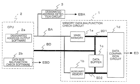
In Fig. 1, the elevator electronic safety syster-n includes a memory data
malfunction check circuit 1 that serves to check the malfunction of memory
data, a CPU 2, and a designated address detection circuit 3 that serves to
check the malfunction of an address bus.
3
CA 02563255 2006-10-05
The memory data malfunction check circuit 1 a includes a main
memory 1 a and an auxiliary memory 1 b ( RAM ) that are arranged in parallel
with each other so as to be allocated to the same address space in a
overlapped manner, data buffer 1 c that serves to avoid the collision of the
output data from the auxiliary memory 1b, and a data comparison circuit 1d
that serves to make a comparison between each piece of data of the main
memory 1 a and the corresponding piece of the auxiliary memory 1 b so as to
check data malfunction.
In addition, though not illustrated herein, the memory data malfunction
check circuit 1 is provided with an error correction code check circuit, as in
a
conventional system.
The CPU 2 includes a designated address output software 2a for
outputting a designated address at the time of data malfunction check, a data
bus malfunction check software 2b that is executed at the time of data bus
malfunction check, and a ROM ( not shown ) for storage of programs.
In the memory data malfunction check circuit 1, the main memory 1 a
and the auxiliary memory 1 b are connected to the CPU 2 through an address
bus BA and a data bus BD, respectively, so that data for an elevator
electronic
safety apparatus is written from the CPU 2, and read out to the CPU 2.
The data bus BD is branched into a main memory data bus BD1 and
an auxiliary memory data bus BD2 in the memory data malfunction check
circuit 1, so that the main memory 1 a and the auxiliary memory 1 b are
connected to the data comparison circuit 1d through the main memory data
bus BD1 and the auxiliary memory data bus BD2, respectively.
A data buffer 1c is interposed in the auxiliary memory data bus BD2.
At the time of checking the malfunction of the memory data, the data
comparison circuit 1 d compares individual pieces of memory data input
through the main memory data bus BD1 and the auxiliary memory data bus
BD2, respectively, and outputs a data malfunction signal ED when it makes a
4
CA 02563255 2006-10-05
determination that there is a malfunction in the memory data.
The designated address detection circuit 3 is connected to the CPU 2
through the address bus BA so as to detect a designated address at the time
of checking the malfunction of the address bus BA, and outputs an address
bus malfunction signal EBA when it is determined that there is a malfunction
in
the address bus BA.
The designated address output software 2a in the CPU 2 operates at
the time of checking the malfunction of the address bus BA, and outputs a
designated address to the designated address detection circuit 3 in a periodic
manner, as will be described later.
The data bus malfunction check software 2a in the CPU 2 operates at
the time of checking the malfunction of the address bus BD, and outputs a data
bus malfunction signal EBD when it makes a determination that there is a
malfunction in the data bus BD.
Fig. 2 specifically shows the data comparison circuit 1d for data
malfunction check in Fig. 1, wherein the data comparison circuit 1d is
composed of a plurality of exclusive OR gates 21, an AND gate 22 and a
D-type latch circuit 23 using a memory read signal RD.
In Fig. 2, the data comparison circuit 1d includes the exclusive OR
gates 21 arranged in parallel with one another, the AND gate 22 that takes the
logical product of the respective output signals of the exclusive OR gates 21,
and the D-type latch circuit 23 that receives an output signal of the AND gate
22 as a D terminal input and output an H ( logic "1" ) level signal as the
data
malfunction signal ED.
Each of the exclusive OR gates 21 receives data from the main
memory data bus BD1 as one input signal, and data from the auxiliary memory
data bus BD2 as the other input signal, and it outputs an L ( logic "0" )
level
signal when both of the input signals coincide with each other, and outputs an
H ( logic "1" ) level signal when both of the input signals are not coincide
with
J
CA 02563255 2006-10-05
each other.
The AND gate 22 takes in the inverted signal of the output signal from
each of the exclusive OR gates 21, and outputs an H ( logic "1" ) level signal
when all the input signals are at an H level ( i.e., the respective output
signals
of the exclusive OR gates 21 are all at an L level ).
The D-type latch circuit 23 operates in response to the memory read
signal RD, so that it changes the level of its output signal ( the data
malfunction
signal ED ) in response to a D terminal input ( the output signal of the AND
gate 22 ), and it is reset to its initial state in response to a reset signal
RST.
Fig. 3 specifically shows the designated address detection circuit 3 for
address bus malfunction check in Fig. 1.
In Fig. 3, the designated address detection circuit 3 includes a plurality
of exclusive OR gates 31 with an H level signal being supplied thereto as one
input signal, a plurality of exclusive OR gates 32 with an L level signal
being
supplied thereto as one input signal, an NAND gate 33 that takes the logical
product of the respective output signals of the exclusive OR gates 31 and the
address strobe signal STR, an NAND gate 34 that takes the logical product of
the respective output signals of the exclusive OR gates 32 and the address
strobe signal STR, a D-type latch circuit 35 that receives an output signal of
the NAND gate 33 as an input signal to its set terminal, a D-type latch
circuit
36 that receives an output signal of the NAND gate 34 as an input signal to
its
set terminal, an AND gate 37 that takes the logical product of the respective
output signals of the D-type latch circuits 35, 36, a D-type latch circuit 38
that
operates in response to a reset signal RST1 of the designated address
detection circuit 3, a D-type latch circuit 39 that operates in response to a
mask
signal MSK of the designated address detection circuit 3, and an OR gate 40
that takes the logical sum of the output signal of the AND gate 37 and the
output signal of the D-type latch circuit 39.
A designated address is input through the address bus BA to the other
G
CA 02563255 2006-10-05
input terminal of each of the exclusive OR gates 31, 32 that are arranged in
parallel with one another.
Each of the exclusive OR gates 31 outputs an L level signal when the
designated address input from the address bus BA is an H level signal,
whereas it outputs an H level signal when the designated address is an L level
signal.
On the contrary, each of the exclusive OR gates 32 outputs an H level
signal when the designated address input from the address bus BA is an H
level signal, whereas it outputs an L level signal when the designated address
is an H level signal.
The output signal of each of the exclusive OR gates 31 is level
inverted and input to the NAND gate 33 together with the address strobe signal
STR.
Similarly, the output signal of each of the exclusive OR gates 32 is
level inverted and input to the NAND gate 34 together with the address strobe
signal STR.
Accordingly, if the address bus BA is sound or normal, the NAND gates
33, 34 each output an H level signal in a periodic and complementary r-nanner
according to a designated address ( "FFFF", "0000" ) periodically input
through
the address bus BA in synchronization with the address strobe signal STR.
The D-type latch circuit 38 has its D input terminal impressed with an L
level signal, so that it is operated by a first reset signal RST1. An output
signal
of the D-type latch circuit 38 is impressed to the respective reset terminals
of
the D-type latch circuits 33, 36.
The D-type latch circuit 39 has its D input terminal impressed with a 0
bit signal BTO ( i.e., it becomes "0" when the mask is turned on, and "1" when
the mask is turned off ) of the data bus BD, so that it is operated according
to a
mask signal MSK.
The respective D-type latch circuits 38, 38 are reset respectively by a
7
CA 02563255 2006-10-05
second reset signal RST2.
When the output signal of the AND gate 37 or the output signal of the
D-type latch circuit 39 indicates an H level, the OR gate 40 outputs an
address
bus malfunction signal EBA.
In the elevator electronic safety system as constructed above, a
malfunction check on the address bus BA according to the designated address
output software 2a and the designated address detection circuit 3 as well as a
malfunction check on the data bus BD according to the data bus malfunction
check software 2b is executed in addition to a data malfunction check
according to the memory data malfunction check circuit 1.
Now, reference will be made in more detail to the above-mentioned
three malfunction check operations according to the first embodiment of the
present invention while referring to Fig. 1 through Fig. 5.
Fig. 4 is a flow chart that shows the processing operation according to
the designated address output software 2a and the designated address
detection circuit 3 in the CPU 2, where there is illustrated an operations
sequence when a designated address is output to the designated address
detection circuit 3 at the time of checking the malfunction of the address bus
BA.
Fig. 5 is a flow chart that shows the processing operation of the data
bus malfunction check software 2b in the CPU 2.
First of all, the data malfunction check operation according to the
memory data malfunction check circuit 1 will be described while referring to
Fig.
1 and Fig. 2.
In the memory data malfunction check circuit 1, the same address
space is allocated to the main memory 1 a and the auxiliary memory 1 b in a
overlapped manner, so when the CPU 2 writes data into the main memory 1a
and the auxiliary memory 1 b, the same data is written into the same address
of
the main memory 1 a and the auxiliary memory 1 b, respectively.
3
CA 02563255 2006-10-05
On the other hand, when the CPU 2 reads out data from the main
memory 1 a and the auxiliary memory 1 b, the data of the main memory 1 a is
read onto the main memory data bus BD1, and passed to the CPU 2 through
the data bus BD, whereas data in the auxiliary memory 1 b is read onto the
auxiliary memory data bus BD2 but it is blocked by the data buffer 1c, as a
result of which it is not sent to the data bus BD.
Accordingly, two memory outputs from the main memory 1 a and the
auxiliary memory 1 b does not conflict with each other, and hence only the
data
of the main memory 1a is passed to the CPU 2, so writing and reading are
executed normally.
Simultaneously with this operation, the main memory data read onto
the main memory data bus BD1 and the auxiliary memory data read onto the
auxiliary memory data bus BD2 are input to the data comparison circuit 1d
where a comparison is carried out between both of these data.
The data comparison circuit 1 d checks data abnormality or malfunction,
and outputs a data malfunction signal ED if abnormality or malfunction
( non-coincidence between these data ) is detected.
Next, a malfunction check operation on the address bus BA according
to the designated address output software 2a and the designated address
detection circuit 3 in the CPU 2 will be described while referring to Fig. 1,
Fig. 3
and Fig. 4.
The CPU 2 repeatedly performs the processing of Fig. 4 ( steps S1
through S4 ) in a periodic manner by executing the designated address output
software 2a by using a designated address for checking ( e.g., "FF" and "00"
in
case of 8 bits ) that is able to verify both the cases of "0" and "1" for each
of all
the bit signals on the address bus BA used in the memory system.
In addition, simultaneously with this, each designated address is
detected by the designated address detection circuit 3 installed on the
address
bus BA.
9
CA 02563255 2006-10-05
When all the designated addresses can not be detected, the
designated address detection circuit 3 makes a determination that there is a
malfunction in the address bus BA, and outputs an address bus malfunction
signal EBA.
In Fig. 4, the CPU 2 first turns on the mask of the designated address
detection circuit 3 ( step S1 ), operates the D-type latch circuit 39 in the
designated address detection circuit 3, and impresses a 0 bit signal BTO ( = 0
)
to the D input terminal.
Subsequently, the CPU 2 resets the designated address detection
circuit 3 by means of a first reset signal RST1 ( step S2 ), and operates the
D-type latch circuit 38.
Then, the CPU 2 reads out a maximum value address "FFFF" for
which the values of the address are all "1" ( or a minimum value address
"0000" for which the values of the address all become "0" ( step S3).
Finally, the CPU 2 turns off the mask of the designated address
detection circuit 3 ( step S4 ), and impresses a 0 bit signal BTO ( = 1 ) to
the D
input terminal of the D-type latch circuit 39 thereby to invert the operating
state
of the D-type latch circuit 39, and then exits the processing routine of Fig.
4.
Next, a malfunction check operation on the data bus BD according to
the data bus malfunction check software 2b in the CPU 2 will be described
while referring to Fig. 1 and Fig. 5.
The CPU 2 repeatedly performs a read and write check operation
according to the processing of Fig. 5 ( steps S11 through S17 ) in a periodic
manner by using designated data for checking ( e.g., set or combined values
such as "AA" and "55", or "01 ", "02", "04", "08", "10", "20", "40", and "80"
in
case of 8 hits ) that is able to verify both the cases of "0" and "1" for each
of all
the bit signals on the data bus BD used in the memory system.
If all the designated data do not coincide in the determination
processing according to the data bus malfunction check software 2a, the CPU
CA 02563255 2006-10-05
2 makes a determination that there is a malfunction in the data bus BD, and
outputs a data bus malfunction signal EBD.
In Fig. 5, first of all, the CPU 2 initializes a variable N specifying the
designated data to "1" ( step S11 ), and writes the Nth ( = 1st ) designated
data
( _ "01" ) into a test address in the RAM ( the main memory 1a and the
auxiliary memory 1 b ) ( step S12 ).
Subsequently, the designated data written in step S12 is read out from
the test address ( step S13 ), and it is determined whether the designated
data
thus read out coincides with the designated data before written ( step S14 ).
When it is determined in step S14 that the designated data after read
out does not coincide with the designated data before written ( that is, NO ),
the CPU 2 assumes that there is a malfunction in the data bus BD, and causes
an abnormal termination, while outputting a data bus malfunction signal EBD
( step S15 ).
On the other hand, when it is determined in step S14 that the
designated data after read out coincides with the designated data before
written ( that is, YES ), the variable N is incremented ( step S16 ), and it
is
further determined whether the variable N is equal to or less than "8" ( step
S17 ).
When it is determined as N ~ 8 in step S17 ( that is, YES ), a return
is performed to the writing processing of the designated data ( step S12 ),
and
then the above-mentioned processing steps S13 through S16 are repeatedly
carried out.
Specifically, the 2nd designated data ( _ "02" ), the 3rd designated data
( _ "02" ), ~ ~ ~ , the 8th designated data ( _ "80" ) are sequentially
written into
the test address in the RAM ( step S12 ), and then read out again (step S13)
so as to determine coincidence or non-coincidence, as stated above ( step
S14 ).
On the other hand, when it is determined as N > 9 in step S17 ( that is,
11
CA 02563255 2006-10-05
NO ), it is assumed that the data bus malfunction check has been executed for
all the pieces of designated data ( N = 1 to 8 ), and that all the pieces of
designated data have coincided between before and after writing, and the CPU
2 normally terminates the processing routine of Fig. 5.
Thus, it is possible to improve the reliability of malfunction check by
performing, in addition to the processing according to the memory data
malfunction check circuit 1 similar to the conventional system, periodic
malfunction check processing on the address bus BA and the data bus BD that
are used when memory is written and read.
i~