Note: Descriptions are shown in the official language in which they were submitted.
CA 02563606 2006-10-16
WO 2005/107351 PCT/US2005/011653
A HOUSING FOR A CIRCUIT THAT IS TO BE~IMPLANTED IN
VIVO AND PROCESS OF MAKING THE SAME
BACKGROUND OF THE INVENTION
1. Field of the invention
[001] The present invention relates to a circuit
housing, and, more specifically, to a housing for a
circuit~designed to be implanted in-vivo (i.e., an
imphantable circuit).
2. Discussion of the Background
{002] There are several applications that require
a circuit to be protected from the environment in
which the circuit is intended to operate. For
example, a human-imphantable glucose sensor circuit
must be~.~housed within. a suitable housing to both
protect the sensor from the human body and to protect
the human body from the sensor: U.S. Pat. No.
6,330.,464; the disclosure of which is incorporated
herein by this reference, discloses such a sensor.
[003] A housing, encasing an implantable circuit
should have at least some of the following
characteristics: (1) the ability to protect the
electronic circuitry of the sensor from the ambient
in-vivo chemical. and. physical environment, (2)~the
ability to protect tissue adjacent to the sensor from
any adverse reaction which could result as a
consequence of contact (or.leachables) from within~the
circuitry - in addition, beyond the adjacent tissue,
1
CA 02563606 2006-10-16
WO 2005/107351 PCT/US2005/011653
the encasement must not permit leachables of any
detectable significance into the general body
environment; (3) the ability to permit wireless
electronic communication between the circuitry and an
external reader~for power and signal; (4) the ability
to permit free passage of wavelengths of light
necessary for optical functioning of the sensor; (5)
the ability to support the surface chemistry required
to form a chemical recognition "front-end"; (6) the
housing should be high volume manufacture-able; (7)
the housing must be non-toxic and "biocompatible"; and
(8) provide a sufficiently high reliability to meet
the specifications of a medical product.
SUMMARY OF THE INVENTION
[004] The present invention provides a housing
that meets many of the criteria outlined above. In
one aspect, the present invention provides a circuit
encased within a completely enclosed polymer housing.
Preferably, the housing is made of an organic polymer,
such as PMMA. In some embodiments, the circuit is
first enclosed within a glass housing which itself is
then enclosed within a second housing, such as a
housing made from an organic polymer. In other
embodiments, the circuit is first encased within a
brick of epoxy and then the epoxy brick containing the
circuit is enclosed within a housing.
[005] In another aspect, the present invention
provides a method for. enclosing a circuit in a polymer
housing. In one embodiment, the method may include
2
CA 02563606 2006-10-16
WO 2005/107351 PCT/US2005/011653
the following steps: (a) placing the circuit in a
mold;~(b) pouring a formulation into the mold so that
the. formulation completely surrounds the circuit,
wherein the formulation comprises monomers.; and (c)
polymerizing the monomers. In step (b), all of the
formulation need not be poured at once. For example,
in some embodiments, the formulation is poured into
the mold 'until the mold is half full and then after a
delay additional formulation is poured into the mold.
In some embodiments, the monomers may be MMA monomers.
The formulation may further comprise pre-polymerized.
PMMA.
[006] In another embodiment, the method may
include the following steps: inserting the circuit
into a polymer housing; injecting an optical epoxy
into the polymer housing to fill the spaces between
the circuit and the inside walls of the housing.(in
some embodiments the injection is from the bottom up
to force out trapped air); capping an open end of the
housing; placing the housing containing the optical
epoxy and the circuit into a pressure vessel and
increasing th.e pressure and temperature within the
vessel; allowing the optical epoxy to cure; and
removing the housing from the pressure vessel,
[007] In another embodiment, the method may
include the following steps: inserting the circuit
into a glass housing; injecting an optical epoxy into
the glass housingto fill the spaces between the
circuit and the inside walls of the housing; injecting
3
CA 02563606 2006-10-16
WO 2005/107351 PCT/US2005/011653
an optical epoxy into a polymer housing; inserting
into the polymer housing the glass housing containing
the circuit; capping an open end of the glass housing;
and capping an open end of the polymer housing.
[008] The above and other features and advantages
of the present invention, as well as the structure and
operation of preferred embodiments of the present
invention, are described in detail below with
reference to the accompanying drawings.
BRIEF DESCRIPTION OF THE DRATnIINGS
[009] The accompanying drawings, which are
incorporated herein and form part of the
specification, help illustrate various embodiments of
the present invention and, together with the
description, further serve to explain the principles
of the invention and to enable a person skilled in the
pertinent art~to make and use the invention. In the
drawings, like reference numbers indicate identical or
functionally similar elements. Additionally, the
left-most digits) of a reference number identifies
the drawing in which the reference number first
appears.
[0010] FIG. 1 illustrates one embodiment of a
circuit assembly according to the present invention.
[0011] FIG. 2 is a flow chart illustrating a
process, according to one embodiment, for encasing a
circuit within a polymer housing.
4
CA 02563606 2006-10-16
WO 2005/107351 PCT/US2005/011653
[0012] FIG. 3 is a cross sectional view of a
circuit assembly according to an embodiment of the
invention.
[0013] FIG. 4 is a flow chart illustrating a
process, according to another embodiment, for encasing
a circuit within a polymer housing.
[0014] FIG. 5 is an exploded view of a circuit
assembly according to an embodiment of the invention.
[0015] FIG. 6 is a cross sectional view of a
circuit assembly according to another embodiment of
the invention.
[0016] FIG. 7 illustrates a circuit assembly
according to another embodiment of the present
invention.
[0017] FIG. 8~is an exploded view of a circuit
assembly according to another embodiment of the
invention.
[0018] FIG. 9 is a flow chart illustrating a
process, according to another embodiment,. for encasing
a circuit within a polymer housing.
[0019] FIGS. IOA~and 10B illustrate a circuit
covered with different amount of epoxy.
DETAILED DESCRIPTION OF THE PREFERRED EMBODIMENT
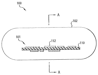
[0020] FIG. 1 illustrates one embodiment of a
circuit assembly 100 according to the present
invention. As shown in FIG. 1, the present invention
provides an assemblage including a circuit 101 housed
CA 02563606 2006-10-16
WO 2005/107351 PCT/US2005/011653
within a fully enclosed housing 102. Preferably, as
shown in FIG. 1, housing 102 is capsule shaped, but
"other shapes may be used. Circuit 101 may be an
electronic circuit having a printed circuit board 110
and one or more electrical and optical components 112
attached to the circuit board 110. Circuit 101 may
include a conventional sensor, such as the sensor
described in U.S, Patent No. 6,304,766. The housing
102 may be a housing made from PMMA, which is a
polymer of methyl methacrylate (MMA) monomers, or from
other organic polymers.
[0021] FIG. 2 is a flow chart illustrating a
process 200,. according to one embodiment, for creating
circuit assembly 100. Process 200 may begin in step
202, where a polymerization initiator is added to a
mold. In step 204, an encasement formulation
containing monomers is poured into the mold (e. g.,
filling the mold halfway). In step 206, circuit 101
is placed in the mold. In step 208, 'more of the
encasement formulation is poured into the mold so that
the circuit is completely immersed in the encasement
formulation. In one-embodiment, the encasement
formulation includes monomers. In one embodiment, the
encasement formulation consists of or essentially
consists of MMA monomers. In this manner, one can
encase circuit 101 in a polymer housing.
[0022] In some situations, for example, situations
where the formulation includes MMA monomers and
circuit 101 is relatively large, circuit 101 can
6
CA 02563606 2006-10-16
WO 2005/107351 PCT/US2005/011653
become severely damaged during the polymerization
process (i.e., .during step 206). The cause of this
damage is. usually attributed to the shrinkage that
occurs naturally during polymerization of MMA. In the
joining of bonds between monomers contained within a
neat solution of MMA, the intermolecular spacing is
reduced within a polymer as the reaction progresses.
This is a well-known phenomena and typical of most, if
not all, polymer reactions. The net volumetric
shrinkage that occurs during the polymerization of
PMMA from neat monomer solution is approximately 140.
[0023] This shrinkage can, in some circumstances,
create a particular problem when using PMMA as a
circuit housing because, as the encasement reaction
progresses, and the viscosity increases as the
shrinkage occurs simultaneously, the electrical
components 112, which are mounted on the circuit board
110 typically with conductive epoxy, are pulled from
the circuit board 110 during the polymerization
process.
[0024] The relative strength of the conductive
epoxy used to hold the components 112 in place, which
conductive epoxy is formulated. primarily and maximally
for its electrical conductance and cure properties,
does not have sufficient mechanical strength to
withstand the pull and stress from PMMA shrinkage as
the encasement reaction progresses. Consequently,
some attempts to encase a circuit from an MMA monomer
7
CA 02563606 2006-10-16
WO 2005/107351 PCT/US2005/011653
encasement formulation result in a non-functional
circuit because of un-repairable mechanical damage.
[0025 To solve this problem, one aspect of the
present invention is a method by which the
polymerization reaction can be conducted without
damage to the encased circuit 101. Because pre-
polymerized PMMA of large molecular weights
(approximately up through 1 million + mw) can be
dissolved in MMA monomer, and because the shrinkage is
a direct result of bonds forming from discrete
monomers, one possible solution is to formulate the
encasement formulation to include a portion of MMA
monomer and a portion of pre-polymerized PMMA
dissolved within the MMA monomer.
[0026] The net shrinkage is proportional to the
amount of monomer which is reacted to become polymer
within the overall volume. Tf the overall encasement
formulation volume, is portioned to include, for
example, about 70o pre-polymerized PMMA, and about 300
un-reacted MMA monomer (into which the 70o PMMA has
been dissolved), then the degree of shrinkage which
occurs drops in direct proportion to the monomer
component within the overall volume. In practice, an
encasement formulation of 1000 MMA monomer shrinks
volumetrically about 140 overall. By dropping the
formulation to only 30o MMA, shrinkage in the amount
of approximately 0'.3 x 14 = 4.3o would be expected. In
practice, approximately 4o shrinkage is measured from
making this improvement.
8
CA 02563606 2006-10-16
WO 2005/107351 PCT/US2005/011653
[0027] Accordingly, the result of altering percent
solids provides an improvement in system stress during
encasement by reducing shrinkage from, for example,
14% to 4o by reformulating MMA/PMMA specifically for
the encasement process. Formulation ratios of 60-800
PMMA in MMA are preferred, although not required,
because of a present practical limitation. Although to
a point, higher ratio values would be expected to
reduce shrinkage proportionately,~and further
reduction in shrinkage may be possible. As a practical
- matter, the solution viscosity.becomes extremely, high
at these Niger ratio levels making the high solids
solution extremely difficult to handle, transfer, etc.
[0028] In some situations, however, even with 40
shrinkage, which is a great improvement over 14o, some
percentage (about 40-50o) of circuits 101 can not
withstand the 4o shrinkage of the encasement. The
surviving circuits tend to have greater amounts of
conductive epoxy to increase mechanical strength
slightly of the surface mounted parts. However,
conductive epoxy is not sufficiently strong, and to
increase the amount used per connection beyond good
manufacturing standards would then create other
problems. Another important consideration is for wire-
bonded circuits. These "frog hair" gold wires are
typically 25 microns in diameter which is about 1/3 to
1/4 the diameter of a typical human hair. Small
amounts of movement relative to the fixed board
components can rip these wires from the attachments.
9
CA 02563606 2006-10-16
WO 2005/107351 PCT/US2005/011653
[0029] Accordingly, in some applications, it is
desirable to mechanically strengthen the circuit 110
to allow it to withstand the remaining shrinkage from
the PMMA encasement cure reaction.
[0030] One way to mechanically strengthen circuit
101 to allow it to withstand the remaining 40
shrinkage from the PMMA (70/30) encasement cure
reaction, is to reinforce the circuit with a pre-
applied epoxy layer. For example, following assembly
of the electrical components to the circuit board and
cleaning of the assembly, an epoxy is applied over the
circuit, which epoxy both under-fills and overfills
the components attached to the circuit board.
Surprisingly, it was discovered that this solution '
works best when the applied epoxy covers the
components in such a way as to result in a relatively
. "smooth" surface topology, but this is not a
requirement. This "smooth" surface topology is
illustrated in FIG. 10A. For comparison, FIG. 10B
shows.a "non-smooth" epoxy coating. As shown in FIG..
10A, the surface 1002 of the epoxy coating is smooth
or substantially smooth.
[003I] Although the epoxy adequately strengthens
circuit 101 against damage from the shrinking polymer,
the resultant stress caused by the remaining 40
shrinkage then becomes manifest as de-lamination
between the adjoining surfaces of epoxy and PMMA
within the final encasement. As mentioned above, it
was discovered that if the surface was smoothed by the
CA 02563606 2006-10-16
WO 2005/107351 PCT/US2005/011653
volume and application of the epoxy pre-coat, not
allowing the PMMA to get a "grip" within the surface
topology, then de-lamination was less likely to occur.
The stress from the 4o remaining shrinkage is then
absorbed as internal stress within the PMMA encasement
body itself. This stress may be removed in a
conventional way by annealing in a final operation.
[0032] Some or all of the epoxy used to reinforce
the circuit 110 may, in some embodiments, include a
light blocking pigment (such as black or wavelength
specific) which prevents unwanted light propagation
and scatter about the circuit, thereby increasing the
optical signal to noise ratio of the system.
[0033] In some embodiments, to prolong the life of
the circuitry 101, it may be desirable to prevent
molecular water vapor that has seeped through the
housing 102 from condensing to become liquid water.
If liquid water cannot form from the water vapor, then
potential ion contaminants present cannot become
solvated, which can lead to circuit failure.
[0034] One way to prevent the water vapor from
condensing is to prevent the formation of heat induced
bubbles in the encasement polymer. MMA monomer is
extremely volatile. The polymerization reaction of
MMA to PMMA is also exothermic. The exothermic heat
yield from a typical reaction begun at room
temperature will commonly increase the temperature as
the reaction progresses to a point where the remaining
un-reacted monomer will boil and create bubbles of all
11
CA 02563606 2006-10-16
WO 2005/107351 PCT/US2005/011653
sizes trapped within the cured polymer. To prevent
any possibility of heat induced micro-bubbles and
voids within the housing where water vapor could
condense, substantial overpressure may be used during
the polymerization reaction. More specifically, in a
preferred embodiment, a mold,containing PMMA/MMA is
placed within a pressure reactor that is then
pressurized to a pressure that exceeds the vapor
pressure of MMA monomer at the polymerization
temperature. This pressurization process both
prevents bubbles and provides a very close mechanical
surface bond with the underlying epoxy coat which does
not delaminate once formed. The housing is clear and
without bubble or void defects to prevent water from
condensing; and as an important byproduct, provides
excellent optical clarity without bubble defect.
[0035] Referring now to FIG. 3, FIG. 3 is a cross
sectional view of circuit assembly 100, according to
one embodiment, along line A. As shown in FIG. 3, the
circuit 101 may be fully encased within a brick of
epoxy 302 (or "epoxy brick 302"), which is encased
within housing 102.
[0036] FIG. 4 is a flow chart illustrating a
process 400, according to another embodiment, for
creating circuit assembly 100. Process 400 may begin
in step 402, where a housing 500 (e.g., a sleeve 500
or tube or other housing having an open end) (see FIG.
5) is created along with a plug 504 for plugging the
opening in the housing. For example, a cylindrical
12
CA 02563606 2006-10-16
WO 2005/107351 PCT/US2005/011653
sleeve 500 and plug 504 may be machined from a polymer
rod, such as a rod of PMMA or other organic polymer.
As shown in FIG. 5, sleeve 500 may have a notch 592
adjacent to the open end 594 of sleeve 500. If sleeve
500 and plug 504 are made from PMMA, the PMMA sleeve
and'plug may be annealed at approximately 80°C for
about four hours (step 403).
[0037] In step 404, epoxy is applied over the
circuit 101 so that the circuit is partially or fully
encased within an epoxy brick 502, thereby forming an
assembly 503. In step 406, assembly 503, sleeve 500
and plug 504 afe cleaned. For example, assembly 503,
sleeve 500 and plug 504 may be cleaned by rubbing a Q-
tip with IPA on the surfaces thereof. In step 408, an
optical epoxy is prepared. EPO-TEK 301-2 Epoxy from
Epoxy Technology of Bi.llerica, MA and other epoxies
may be used as the optical epoxy.
[0038] In step 410, the circuit encased within the
epoxy brick (i.e., assembly 503) is placed into the
sleeve 500. In step 412, the prepared optical epoxy
is injected (i.e., introduced) into sleeve' 500.
Preferably, no bubbles in the optical epoxy are formed
during step 412. In step 414, the plug 504 is placed
into the open end of sleeve 500, thereby sealing the
open end of the sleeve.
[0039] FIG. 6 is a cross sectional view, according
to one embodiment, of the circuit assembly 100 along
line A after step 414 is performed. In the embodiment
shown in FIG. 6, the circuit 101 is fully encased
13
CA 02563606 2006-10-16
WO 2005/107351 PCT/US2005/011653
within an epoxy brick 502. The epoxy brick 502, which
houses circuit 101 is placed within sleeve 500, which
may be a cylindrical sleeve. V~lhen sleeve 500 is a
cylindrical sleeve and when circuit 101 is fully
encased within the epoxy brick, it is preferable that
the distance between the upper right hand corner and
lower left corner of epoxy brick 502 be equal to or
slightly less than the inner diameter of sleeve 502.
That is, in some embodiments it is preferable that w =
sqrt((d*d)-(h*h)), where w is the width of assembly
503, h is the height of assembly 503, and d is the
inner diameter of sleeve 500.~~ In embodiments where
the assembly 503 does not have a uniform width or has
a circular shaped cross section, then the maximum
width of the assembly may be equal to or slightly less
than the inner diameter. As illustrated in FIG. 6,
the optical epoxy (e. g., a refractive index (RI)
matching epoxy) fills spaces between assembly 503 and
sleeve 500.
[0040) Referring back to FIG. 4, in step 416, the
new assembly (i.e., the sealed sleeve containing the
epoxy and assembly 503) is placed into a pressure
vessel. In step 418, the pressure within the vessel
is increased to about 125psi using Nitrogen or other
inert gas. In step 420, the optical epoxy is cured
for an amount of time (e.g., 20 hours) at a
predetermined.temperature (e.g., 40°C). After the
predetermined amount of time has elapsed, the assembly
14
CA 02563606 2006-10-16
WO 2005/107351 PCT/US2005/011653
is removed from the pressure vessel and then final
machined (step 422).
[0041] The method described above allows the
possibility of annealing a PMMA housing before
encasement without putting any additional stress on
the circuit 101.
[0042] FIG. 7 illustrates an alternative circuit
assembly 700 of the present invention. Circuit
assembly 700 is similar to circuit assembly 100 in
that assembly 700 includes a circuit 101 housed within
a housing 102. However, in assembly 700, the circuit
101 is also housed within a glass housing 702 (e.g., a
tube or other shaped housing), which itself is housed
within the housing 102. The glass housing~702, in
some embodiments, is closed at one end and open at the
opposite end. The open end may be plugged by a glass
ball 704 or other suitable plug. FIG. 8 is an
exploded view showing the components of assembly 700,
according to one embodiment. Glass housing 702, in
some embodiments, may be constructed from an infra-red
(IR) blocking glass.
[0043] FIG. 9 is a flow chart illustrating a
process 900, according to one embodiment, for making
assembly 700. Process 900 may begin in step 902,
where a sleeve and a plug, such as. sleeve 500 and plug
504, are created.
[0044] In step 904, the sleeve and plug are
annealed. The sleeve and plug may be annealed at 80°C
CA 02563606 2006-10-16
WO 2005/107351 PCT/US2005/011653
for about four hours. In step 906, the components
(e. g., sleeve 500, plug 504, glass housing 702, glass
ball 704, epoxy brick 502, etc.) are cleaned. For
example, sleeve 500 and plug 504 may be cleaned in an
ultrasonic bath with IPA followed by a rinse step, and
glass housing 702 and glass ball 704 may also be
cleaned ultrasonically with KOH/alcohol solutions and
then rinsed with water.
['0045] In step 908, a bonding agent is applied to
the glass housing 702 and glass ba11.704. The bonding
agent used may be trimethoxy [2-(7-oxabicyclo
[4.1.0]kept-3-yl)ethyl] silane, which may be purchased
from Sigma-.Aldrich Corporation (catalog no. 413321)
[0046] In step 910, a batch of optical epoxy is
prepared. In step 912, the epoxy coated circuit board
is inserted into the glass housing. In step 914, some
of the prepared epoxy is injected into the glass
housing 702.
[0047] In step 916, some of the prepared epoxy is
injected into the sleeve 500. In step 918, glass
housing 702, which houses the circuit, is inserted
into an open end of the sleeve. In step 920, the
glass ball 704~is inserted into the open end of glass
housing 702, thereby sealing the open end of the glass
housing. In step 922, the plug 504 is used to seal
the open end of the sleeve.
[0048] In step 924, the sealed sleeve, which houses
glass housing 702, which houses the circuit 101; is
16
CA 02563606 2006-10-16
WO 2005/107351 PCT/US2005/011653
placed into a pressure vessel where the pressure is
increased to about 125psi using an inert gas and the
temperature is increased to about 40°C. After about
20 hours, the pressure is gradually reduced and the
assembly is removed from the pressure vessel and then
final machined (step 926).
[0049] Although the above described processes are
illustrated as a sequence of steps, it should be
understood by one skilled in the art that at least
some of the steps need not be performed in the order
shown, and, furthermore, some steps may be omitted and
additional steps added.
[0050] While various embodiments/variations of the
present invention have been described above, it should
be understood that they have been presented by way of
example only, and not limitation. 'Thus, the breadth
and scope of the present invention should not be
limited by any of the above-described exemplary
embodiments, but should be defined only in accordance
with the following claims and their equivalents.
17