Note: Descriptions are shown in the official language in which they were submitted.
CA 02563655 2011-12-23
1
TITLE OF THE INVENTION
TELECOMMUNICATIONS CONNECTOR
FIELD OF THE INVENTION
[002] The present invention relates to a telecommunications connector. In
particular, the present invention relates to a telecommunications connector
comprised of a plurality of contact points having a compensating element at
the point of contact.
BACKGROUND TO THE INVENTION
[003] Connectors, or connector jacks, are adapted to receive plugs for the
interconnection of telecommunication cables and equipment, a good example
thereof being connectors and plugs which conform to the ubiquitous RJ-45
standard. As known in the art, as the plug is inserted into the connector a
series of terminal contacts exposed along an edge of the plug come into
contact with a corresponding series of contact elements disposed in the
connector housing. Each of the contact elements typically forms a portion of a
rigid tine manufactured from a conductive material such as nickel or gold
plated steel or the like. The individual tines are in turn mounted in an
isolating
support and include a bendable portion such that, as the terminal contacts
come into contact with the contact elements the contact elements are
retracted, while at the same bringing a countering force to bear to improve
the
interconnection.
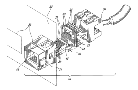
CA 02563655 2006-10-18
WO 2005/101579 PCT/CA2005/000588
2
[0041 As transmission bandwidths and transfer rates increase in data
communication systems, compensation for crosstalk noise becomes
increasingly important. As wiring and cabling structures and configurations
are
improved to satisfy the low noise requirements of these data transfer
technologies, connectors terminating such transfer lines must also meet the
same requirements.
[005] Connectors conforming to the welt-known RJ-45 standards are good
examples of connectors being subject to crosstalk noise (NEXT: Near End
Crosstalk, FEXT: Far End Crosstalk) between adjacent conductor pairs, as
conductor pairs (usually four pairs) within such connectors are not
symmetrically configured for all pair combinations. In order to fully
compensate for common and differential mode crosstalk noise arising in
signals transferred through such a plug/connector interface, in other words,
for the above connector to operate in an optimal balanced mode, reactances
between all conductors of each pair must be equal. Presently, pairs identified
by the pins 3-6 and 4-5 are typically well balanced in prior art plugs and
connectors, providing adequate compensation for common and differential
mode noise between these pairs. On the other hand, the capacitive couplings
between the pairs 1-2 and 3-6 and the pairs 3-6 and 7-8 are not equal for all
conductors, which gives rise to, among others, mode conversion noise or
crosstalk between the pairs (e.g. differential mode to common mode NEXT
and vice-versa), a significant problem when attempting to comply with
increasingly demanding industry standards.
1006] The prior art reveals a variety of compensation networks and methods
for mode conversion noise or crosstalk between pairs- However, one
drawback of these prior art networks is that the compensating elements, be
they inductive or capacitive, are located away from the point of contact
between the terminal contacts of the plug and the contact elements of the
connector.
CA 02563655 2006-10-18
WO 2005/101579 PCT/CA2005/000588
3
SUMMARY OF THE INVENTION
[007] The present invention addresses the above and other drawbacks by
providing a contact element for use in a connector, the connector comprising
a socket adapted for receiving a cable plug comprising a terminal contact. The
contact element comprises a flexible dielectric substrate; and a first
conductive strip on a first surface of the substrate- When the plug is
inserted
into the socket, the terminal contact comes into contact with the conductive
strip.
[008] Additionally there is provide a contact mechanism for use in a
connector, the connector comprising a socket adapted to receive a plug
comprising a plurality of terminal contacts. The mechanism comprises a
flexible dielectric substrate, and a plurality of first conductive strips
disposed
on a first surface of the substrate, wherein when the plug is inserted into
the
socket, each of the terminal contacts comes into contact with a predetermined
one of the conductive strips.
[009] There is also provided a connector for interconnection with a cable
plug, the plug comprising a plurality of terminal contacts. The connector
comprises a socket adapted for receiving the plug, and a plurality of contact
elements disposed in the socket, each of the elements comprised of a
conductive strip on a first surface of a flexible dielectric substrate. When
the
cable plug is inserted into the socket, each of the terminal contacts comes
into
contact with a predetermined one of the contact strips.
[010] Furthermore, there is provide a compensating connector for
interconnection with a cable plug, the plug comprising a plurality of terminal
contacts. The connector comprises a socket adapted for receiving the plug, a
plurality of contact elements disposed in the socket, each of the contact
elements comprising a conductive strip, and a compensation network
comprised of a plurality of compensating elements, wherein each of the
CA 02563655 2010-02-04
4
compensating elements is located adjacent to one of the contact elements.
When the plug is inserted into the socket, each of the terminal contacts comes
into contact with a predetermined one of the conductive strips.
[011] Also, there is provided a contact element for use in a compensating
connector, the connector comprising a socket adapted for receiving a cable
plug comprising a terminal contact. The contact element comprises a
dielectric support, and a compensating element comprising a conductive strip
on a surface of the support. When the plug is inserted into the socket, the
terminal contact comes into contact with the conductive strip.
[012] Additionally, there is provide a compensating connector for
interconnection with a cable plug terminating a telecommunications cable
comprised of a plurality of conductors arranged in pairs, the plug comprising
a
plurality of terminal contacts terminating a predetermined one of the
conductors. The connector comprises a socket adapted for receiving the plug,
a plurality of contact elements disposed in the socket, each of the contact
elements comprising a conductive strip, and a compensation network
comprised of a plurality of compensating elements, wherein each of the
compensating elements is located adjacent to one of the contact elements.
When the plug is inserted into the socket, each of the terminal contacts comes
into contact with a predetermined one of the conductive strips.
BRIEF DESCRIPTION OF THE FIGURES
[013] Figure 1 is a perspective view of an RJ-45 socket and plug assembly in
accordance with an illustrative embodiment of the present invention;
[014] Figure 2 provides an exploded view of a connector in accordance with
an illustrative embodiment of the present invention;
[015] Figure 3 provides a raised front perspective view of a support structure
CA 02563655 2006-10-18
WO 2005/101579 PCT/CA2005/000588
with flexible PCB attached in accordance with an illustrative embodiment of
the present invention;
[016] Figures 4A provides a top view of a flexible PCB detailing the traces on
a top surface of the PCB in accordance with an illustrative embodiment of the
present invention;
[017] Figures 4B provides a top view of the flexible PCB in Figure 4A
detailing the traces on a bottom surface of the PC13 in accordance with an
illustrative embodiment of the present invention;
[0181 Figure 4C is a sectional view along 4C in Figure 4A;
[0191 Figure 5 provides a schematic view of a plug and compensating
network in accordance with an illustrative embodiment of the present
invention;
[0201 Figure 6 provides a raised front perspective view of a flexible PCB in
accordance with an illustrative embodiment of the present invention;
[021] Figure 7 provides a raised front perspective view of a support structure
with a PCB attached in accordance with an alternative illustrative embodiment
of the present invention;
[022] Figure 8 provides a side perspective view (from below) of a contact
assembly and compensating network in accordance with a second alternative
illustrative embodiment of the present invention; and
[0231 Figure 9 provides a raised rear perspective view of a connector in
accordance with a third illustrative embodiment of the present invention.
CA 02563655 2010-02-04
6
DETAILED DESCRIPTION OF THE ILLUSTRATIVE EMBODIMENTS
[024] Referring now to Figure 1, an illustrative embodiment of a connector,
generally referred to using the reference numeral 10, will now be described.
As known in the art user equipment as in 12 typically gains access to a local
area network (LAN) or the like (not shown) via a network cable 14 comprised
of a plurality of twisted pairs of conductors (not shown). The network cable
14
is terminated by a plug 16 which is adapted for insertion into (and removal
from) the connector 10. The connector 10 terminates a communications cable
18 which, at an opposite end, is terminated by other networking equipment
such as switches, hubs, routers, repeaters and the like (all not shown). Both
the network cable 14 and the communications cable 18 are comprised of
typically the same number of twisted pairs of conductors as in 20.
[025] Still referring to Figure 1, the connector 10, which is typically
mounted
flush with a wall or the like (not shown) behind which the communications
cable 18 is hidden, is inserted into a face plate 22 and retained securely
therein by a pair of tabs 24 moulded or otherwise formed in an outer surface
of the connector 10 which mate with similar interlocking portions 26 moulded
into the face plate 22. For jacks and plugs which conform to the RJ-45
standard, a series of eight (8) connector contact strips (not shown) are
disposed within the connector 10 which individually terminate the twisted
pairs
of conductors 20 of the communications cable 18. Similarly, the eight (8)
conductors within the cable 14 are individually terminated by a series of
eight
(8) terminal contacts as in 28 exposed along a forward face 30 of the plug 16.
When the plug 16 is inserted into the connector 10, the connector contact
strips of the connector 10 are brought into contact with the terminal contacts
28 of the plug 16 thereby providing a conductive path between plug 16 and
connector 10 and as a result, interconnecting the conductors of the cable 14
with those of the communication cable 18.
[026] Referring now to Figure 2, connectors as in 10 are typically modular
CA 02563655 2006-10-18
WO 2005/101579 PCT/CA2005/000588
7
and designed for snapping into a face plate (or panel) 22 provided with one or
more cut away connector receptacles as in 32 therein, or alternatively for
mounting directly on printed circuit boards or the like (not shown) as part of
a
larger circuit assembly. Illustratively, the connector 10 is comprised of a
two
part housing comprised of the forward part 34 and a rearward part 36 both
manufactured from a suitable rigid non-conducting material such as plastic. A
series of contact elements 38 comprised of contact strips 40 are disposed
within the housing and enclosed therein when the forward part 34 is
assembled to the rearward part 36. The series of contact strips 40 are
illustratively etched on a first surface 42 of a Printed Circuit Board (PCB)
44
manufactured from a non-conductive (dielectric) and illustratively flexible
material such as polymicle, Kapton , etc., and coated with a conductive
material such as copper or aluminium to form a contact assembly. As known
in the art, lithographic techniques can be used to selectively remove a
surface
layer of conductive material from a PCB leaving conductive traces supported
by a non-conductive substrate. The exposed series of contact strips 40 are
typically covered in a conductive material having high oxidation potential,
such
as gold.
[0271 As will now be apparent to those of ordinary skill in the art, as a
cable
plug (not shown) is inserted into the plug opening 46, each of the contacts
within the cable plug will press against a complementary one of the series of
contact strips 40. Given the flexible nature of the PCB 44, the series of
contact strips 40 will tend to deflect away from the cable plug. In order to
ensure that good contact is maintained between the contacts disposed within
the plug and the series of contact strips 40, a rigid support structure 48,
for
example manufactured from a non-conductive material such as plastic, is
provided around which the flexible PCB 44 is wrapped. A series of non-
conductive supporting blades with limited flexibility as in 50 are mounted at
a
first end 52 to the support structure 48, each of the blades as in 50
positioned
under one of the series of contact strips 40. The glades 50 provide an
independent countering force tending to bias the series of contact strips 40
CA 02563655 2006-10-18
WO 2005/101579 PCT/CA2005/000588
8
towards the contacts of the cable plug and thereby ensuring a reliable contact
when the cable plug is inserted into the assembly 10. Additionally, to improve
the flexibility of the series of contact strips 40 relative to one another,
the
material between adjacent contact strips 40 is removed during fabrication of
the PCB 44.
[028] Referring now to Figure 3, each of the series of contact strips 40 is in
contact with a particular Insulation Displacement Connector (IDC) terminal as
in 54. As is Known in the art, when a small gauge insulated wire as in 56 is
inserted between the bifurcated conductive blades 58, 60 of an IDC terminal
54, an incision is made in the insulation 62 of the wire 56 allowing the
conductive blades 58, 60 to come into contact with the conductor 64 of the
wire 56.
[025] Note that, although the present illustrative embodiment discloses the
use of IDC terminals, alternatively the IDC terminals could be replaced with
other types of terminals, for example rigid contact pins, thereby allowing the
connector 10 to be soldered directly to a PCB or the like (not shown).
[030] Referring now to Figure 4A and Figure 413. a flexible contact assembly
66 will now be described. The series of contact strips 40 are interconnected
with the contact pads as in 68 of the IDC terminals (54 in Figure 3) via a
series of traces as in 70 etched onto the first surface 72 and a second
surface
74 of the PCB 44, Additionally, a compensating network 76 comprised of a
series of selectively interconnected capacitive compensating elements is
provided for.
[031] Referring pack to Figure 1 in addition to Figures 4A and 413, by
adjusting the lays of the twisted pairs of conductors within the cables as in
14
and 18, and in some cases providing shielding between the twisted pairs of
conductors, the design of the cables as in 14 and 18 has been optimised in
order to minimise cross talk between the conductors. However, as is Known in
CA 02563655 2006-10-18
WO 2005/101579 PCT/CA2005/000588
9
the art, elements such as connectors 10, cables 14, 18 and plugs 16 disturb
this optimisation by introducing parasitic reactances into the transmission
path
of signals, thereby causing unbalanced behaviour in regards to cross talk,
noise immunity, etc. which adversely affect the performance of a the
communications system which these elements form part of. Additionally,
untwisting the twisted pairs as well as the presence of metal contacts at.the
connector 10/plug 14 boundary also disturbs this optimisation and introduces
stray or parasitic reactances which must be dealt with (or compensated for) if
high data transfer rates are to be maintained. Also, adjacent conductors are
coupled to one another to some degree and in this manner cross-talk is
introduced into the communications signals. The compensating network 76
selectively couples the twisted pairs of conductors (reference 20 in Figure 1)
through the introduction of inductive and capacitive reactances which
compensate for these parasitic reactances, thereby improving performance,
especially at high frequencies, in terms of reduced cross talk, reduced noise,
etc. As known in the art, such a compensation network can be formed by
combinations of capacitive compensating elements and/or inductive
compensating elements.
(032] Referring now to Figure 4C, each capacitive compensating element 78
is comprised of a first contact plate provided by the contact strip 40 etched
into the first surface 72 of the PCB 44 and a second contact plate 82 which is
etched onto the second surface 74 of the PCB 44. As will now be understood
by a person of ordinary skill in the art, the combination of the dielectric
material of the PCB 44 sandwiched between the contact strip 40 and the
second contact plate 82 provides for a capacitive compensating element 78.
One great advantage of this construction is that the compensating elements
as in 78 are located at the point of contact between the connector 10 and plug
(not shown) which in turn greatly improves the high frequency behaviour of
the compensating network 76.
[033] Referring back to Figures 4A and 413, in order to provided for inductive
CA 02563655 2006-10-18
WO 2005/101579 PCT/CA2005/000588
compensating elements, overlapping inductive loops must be set up. As will
be apparent to a person of ordinary skill in the art, the amount of inductive
coupling will in part be a function of the area of overlap between overlapping
inductive loops. Additionally, inductive coupling can be either forward or
inverse, depending on the direction of current flowing in both the loops.
Referring to Figure 1 in addition to Figures 4A and 4B, when a plug 16 is
inserted in the connector 10, the terminal contacts 28 will come into contact
with predetermined ones of the contact strips 40 in the contact zone 84. In
particular, a path will be set up between contact strip (or pin) 3 (reference
403)
and its associated contact pad 683 via a through hole contact 86 and a trace
703. Of note is that the path of the trace 703 is above contact strip (or pin)
5
(reference 40s on Figure 4A). Similarly, a path will be set up between contact
strip (or pin) 6 (reference 406) and its associated contact pad 686 via a
through hole contact 88 and a trace 706. Of note is that the path of the trace
706 is above contact strip (or pin) 4 (reference 404 on Figure 4A). In this
manner a pair of overlapping inductive loops is set up between pairs 3-6 and
pairs 4-5 causing inductive coupling which is proportional to the space
between pin 4 (reference 404) and pin 5 (reference 406). A similar inductive
coupling is set up between the traces 704, 705 of pin pairs 4-5 (references
404
and 405) and the traces 703r 706 of pin pairs 3-6 (references 403 and 406) in
a
region 90 on the PC board 44 indicated by the dashed box. However, in this
second case the inductive loop is reversed.
[0341 Note that although the present illustrative embodiment describes a
flexible PCB 44 having two conductive layers separated by a dielectric
substrate, a person of ordinary skill in the art will understand that a
multilayer
PCB, wherein a plurality of conductive layers are separated by a plurality of
dielectric substrates, could also be used.
1035] In connectors, cables and plug assemblies according to the RJ-45
specifications, eight (8) conductors are arranged in pairs which are twisted
together to form the twisted pairs widely used in telecommunications systems.
CA 02563655 2010-02-04
11
Referring now to Figure 5, an RJ-45 plug can be modelled as a series of
terminal contacts terminating a series of conductors 94 and between which a
series of parasitic capacitances as in 96 have been introduced. When the plug
16 is inserted into the connector 10, the series of terminal contacts come
into
contact with the contact strips as in 40 which also form the first contact
plates
of the capacitive compensating elements 78. As discussed hereinabove, the
compensating elements 78 are arranged as a compensating network 76
which is designed in a manner to compensate for, or balance, adverse effects
which would otherwise be introduced by the parasitic capacitances 96. In this
regard, and still referring to Figure 5, illustratively the series of
capacitive
compensating elements designated 78, are compensating for the differential
parasitic capacitances 96. Additionally, a second series capacitive
compensating elements (designated 782, 783 and 784) can optionally be
added to compensate for the common mode noise signal generated by the
combination of the parasitic capacitances 96 and the compensating elements
781. Note that other configurations of capacitive compensating elements is
possible. Additionally, inductive compensating elements such as those
described above can be used in combination with the capacitive
compensating elements as described, with appropriate modifications to the
compensating network 76.
[036] To balance the connector 10/plug 16 interface, compensating
(balancing) elements can be integrated into the connector 10 to form the
compensation network 76 that will counter the introduced parasitic
capacitances 96. Such a compensation network 76 can be fabricated from a
combination of compensating elements as in 78 including, for example, one or
more capacitive elements. In an illustrative embodiment all the compensating
elements 78 are capacitors having a value between about 360 15
femtofarads. Necessarily, by placing the compensating elements as in 78
close to the point of introduction of the aforementioned parasitic
capacitances
96 (i.e. at the point of contact between the terminal contacts and the
connector contact strips 40), the compensation can be improved (as time-
CA 02563655 2006-10-18
WO 2005/101579 PCT/CA2005/000588
12
shifted corrections to transferred signals are necessarily delayed from their
point of necessity and thus produce unwanted perturbations in the corrected
signals).
[037] Referring now to Figure 6 in addition to Figure 2, during assembly the
PCI3 44 is formed to fit the support structure 48. Referring now to Figure 7,
however, in an alternative construction of the support structure 48, a similar
connector 10 can be assembled without significantly bending the PCB 44.
This would allow the use, for example, of more rigid PCl3 constructions, for
example those manufactured from thin sheets of FR4 epoxy laminate. The
PCB 44 of Figure 7 also has the advantage that the interconnecting traces
(not shown) between the series of contacts 40 and the IJC terminals as in 54
are somewhat shortened.
[038] Referring to Figure 8, in a second alternative embodiment, the non-
conductive supporting blades as in 50 of Figure 2 could be replaced by a
series of metal tines 98. The tines 98 could be used to support the PCI3 44 of
Figures 4A and 46 with provision of a suitable isolating dielectric between
the
tines 98 and the PCB 44. Alternatively, the compensating elements,
illustratively as in 78, can be formed directly an the tines 98, for example
using a suitable non-conductive adhesive (not shown). In this regard, the
tines
98 provide the first contact plate of the compensating elements 78, with
provision of a suitable dielectric between the second contact plates 82 and
the
tines 98 (for example, a strip of dielectric material disposes between the
surface of the tines 98 and second contact plate 82. The second contact
plates 82 of the compensating elements 78 are interconnected with the first
contact plates formed by the tines 98, illustratively using a series of small
gauge wires as in 100, in order to form a compensating network.
[039] Referring now to Figure 9, the use of a flexible PCI3 44 also allows for
variations in the manner in which the IDC terminals as in 54 are arranged
without any significant modifications to the PCB 44. This allows, for example,
CA 02563655 2011-12-23
13
for improved termination of the cable 102, for example by reducing the
amount the individual wires 56 of the twisted pairs must be unwound prior to
insertion of the wires 56 between the bifurcated conductive blades 58, 60 of
the IDC terminals 54. Improvement of the interconnection between cable 102
and connector 10 in turn provides for improved performance.