Note: Descriptions are shown in the official language in which they were submitted.
CA 02563730 2010-06-15
1
FLUID EJECTION DEVICE WITH IDENTIFICATION CELLS
Background
An inkjet printing system, as one embodiment of a fluid ejection system,
may include a printhead, an ink supply that provides liquid ink to the
printhead,
and an electronic controller that controls the printhead. The printhead, as
one
embodiment of a fluid ejection device, ejects ink drops through a plurality of
orifices or nozzles. The ink is projected toward a print medium, such as a
sheet
of paper, to print an image onto the print medium. The nozzles are typically
arranged in one or more arrays, such that properly sequenced ejection of ink
from the nozzles causes characters or other images to be printed on the print
medium as the printhead and the print medium are moved relative to each other.
CA 02563730 2010-06-15
2
In a typical thermal inkjet printing system, the printhead ejects ink drops
through nozzles by rapidly heating small volumes of ink located in
vaporization
chambers. The ink is heated with small electric heaters, such as thin film
resistors referred to herein as firing resistors. Heating the ink causes the
ink to
vaporize and be ejected through the nozzles.
To eject one drop of ink, the electronic controller that controls the
printhead activates an electrical current from a power supply external to the
printhead. The electrical current is passed through a selected firing resistor
to
heat the ink in a corresponding selected vaporization chamber and eject the
ink
through a corresponding nozzle. Known drop generators include a firing
resistor,
a corresponding vaporization chamber, and a corresponding nozzle.
In fluid ejection device it is desirable to have several characteristics of
each print cartridge easily identifiable by a controller. Ideally the
identification
information should be supplied directly by the print cartridge. The
"identification
information" provides information to the controller to adjust the operation of
the
printer and ensures correct operation.
As the different types of fluid ejection devices and their operating
parameters increase, there is a need to provide a greater amount of
identification
information. At the same time, it is not desirable to add further
interconnections
to the flex tab circuit or to increase the size of the die to provide such
identification information.
For these and other reasons, there is a need for the present invention.
Summary of the Invention
Accordingly, in one aspect of the present invention there is provided a
fluid ejection device comprising: an identification line; and identification
cells
electrically coupled to the identification line, wherein each of the
identification
cells comprises a memory circuit and a memory element, wherein each memory
circuit is adapted to receive and respond to signals to selectively store a
value in
the memory circuit, wherein the value determines whether the identification
cell
is responsive to signals received on the identification line to perform at
least one
of the following: read the memory element; and program the memory element.
According to another aspect of the present invention there is provided a
method of programming a fluid ejection device, comprising: receiving a program
CA 02563730 2010-06-15
2a
signal; receiving enabling signaling at an identification cell; responding to
the
received enabling signaling to provide an enabling value; and storing the
enabling value that selectively enables the identification cell to be
programmed
via the program signal.
According to yet another aspect of the present invention there is provided
a method of reading a fluid ejection device, comprising: receiving a read
signal;
receiving enabling signaling at an identification cell; responding to the
received
enabling signaling to provide an enabling value; and storing the enabling
value
that selectively enables the identification cell to be read via the read
signal.
According to still yet another aspect of the present invention there is
provided a fluid ejection device comprising: an identification line; and a
plurality
of cells, each comprising: a memory element coupled to the identification
line; a
first switch coupled to the memory element, wherein the switch in a stored
charged state allows the memory element to respond to signals received on the
identification line; and a second switch coupled with first switch, the second
switch discharging the stored charge state of the first switch to prevent the
memory element from responding to the signals received on the identification
line.
Brief Description of the Drawings
Figure 1 illustrates one embodiment of an inkjet printing system.
Figure 2 is a diagram illustrating a portion of one embodiment of a
printhead die.
Figure 3 is a diagram illustrating a layout of drop generators located
along an ink feed slot in the one embodiment of a printhead die.
Figure 4 is a diagram illustrating one embodiment of a firing cell
employed in one embodiment of a printhead die.
CA 02563730 2006-10-18
WO 2005/105451 PCT/US2005/011395
3
Figure 5 is a schematic diagram illustrating one embodiment of an ink jet
printhead firing cell array.
Figure 6 is a schematic diagram illustrating one embodiment of a pre-
charged firing cell.
Figure 7 is a schematic diagram illustrating one embodiment of an ink jet
printhead firing cell.array.
Figure 8 is a timing diagram illustrating the operation of one embodiment
of a firing cell array.
Figure 9 is a schematic diagram illustrating one embodiment of an
identification cell in one embodiment of a printhead die.
Figure 10 is a layout diagram illustrating one embodiment of a portion of
a printhead die.
Figure 11 is a flow chart illustrating one embodiment of a manufacturing
process employing selected identification cells in certain embodiments of a
printhead die.
Detailed Description
In the following detailed description, reference is made to the
accompanying drawings which form a part hereof, and in which is shown by way
of illustration specific embodiments in which the invention may be practiced.
In
this regard, directional terminology, such as "top," "bottom," "front,"
"back,"
"leading," "trailing," etc., is used with reference to the orientation of the
Figure(s)
being described. Because components of embodiments of the present
invention can be positioned in a number of different orientations, the
directional
terminology is used for purposes of illustration and is in no way limiting. It
is to
be understood that other embodiments may be utilized and structural or logical
changes may be made without departing from the scope of the present
invention. The following detailed description, therefore, is not to be taken
in a
limiting sense, and the scope of the present invention is defined by the
appended claims.
Figure 1 illustrates one embodiment of an inkjet printing system 20.
Inkjet printing system 20 constitutes one embodiment of a fluid ejection
system
CA 02563730 2006-10-18
WO 2005/105451 PCT/US2005/011395
4
that includes a fluid ejection device, such as inkjet printhead assembly 22,
and a
fluid supply assembly, such as ink supply assembly 24. The inkjet printing
system 20 also includes a mounting assembly 26, a media transport assembly
28, and an electronic controller 30. At least one power supply 32 provides
power to the various electrical components of inkjet printing system 20.
In one embodiment, inkjet printhead assembly 22 includes at least one
printhead or printhead die 40 that ejects drops of ink through a plurality of
orifices or nozzles 34 toward a print medium 36 so as to print onto print
medium
36. Printhead 40'is one embodiment of a fluid ejection device. Print medium 36
may be any type of suitable sheet material, such as paper, card stock,
transparencies, Mylar, fabric, and the like. Typically, nozzles 34 are
arranged in
one or more columns or arrays such that properly sequenced ejection of ink
from nozzles 34 causes characters, symbols, and/or other graphics or images to
be printed upon print medium 36 as inkjet printhead assembly 22 and print
medium 36 are moved relative to each other. While the following description
refers to the ejection of ink from printhead assembly 22, it is understood
that
other liquids, fluids or flowable materials, including clear fluid, may be
ejected
from printhead assembly 22.
Ink supply assembly 24 as one embodiment of a fluid supply assembly
provides ink to printhead assembly 22 and includes a reservoir 38 for storing
ink. As such, ink flows from reservoir 38 to inkjet printhead assembly 22. Ink
supply assembly 24 and inkjet printhead assembly 22 can form either a one-way
ink delivery system or a recirculating ink delivery system. In a one-way ink
delivery system, substantially all of the ink provided to inkjet printhead
assembly
22 is consumed during printing. In a recirculating ink delivery system, only a
portion of the ink provided to printhead assembly 22 is consumed during
printing. As such, ink not consumed during printing is returned to ink supply
assembly 24.
In one embodiment, inkjet printhead assembly 22 and ink supply
assembly 24 are housed together in an inkjet cartridge or pen. The inkjet
cartridge or pen is one embodiment of a fluid ejection device. In another
embodiment, ink supply assembly 24 is separate from inkjet printhead assembly
CA 02563730 2006-10-18
WO 2005/105451 PCT/US2005/011395
22 and provides ink to inkjet printhead assembly 22 through an interface
connection, such as a supply tube (not shown). In either embodiment, reservoir
38 of ink supply assembly 24 may be removed, replaced, and/or refilled. In one
embodiment, where inkjet printhead assembly 22 and ink supply assembly 24
5 are housed together in an inkjet cartridge, reservoir 38 includes a local
reservoir
located within the cartridge and may also include a larger reservoir located
separately from the cartridge. As such, the separate, larger reservoir serves
to
refill the local reservoir. Accordingly, the separate, larger reservoir and/or
the
local reservoir may be removed, replaced, and/or refilled.
Mounting assembly 26 positions inkjet printhead assembly 22 relative to
media transport assembly 28 and media transport assembly 28 positions print
medium 36 relative to inkjet printhead assembly 22. Thus, a print zone 37 is
defined adjacent to nozzles 34 in an area between inkjet printhead assembly 22
and print medium 36. In one embodiment, inkjet printhead assembly 22 is a
scanning type printhead assembly. As such, mounting assembly 26 includes a
carriage (not shown) for moving inkjet printhead assembly 22 relative to media
transport assembly 28 to scan print medium 36. In another embodiment, inkjet
printhead assembly 22 is a non-scanning type printhead assembly. As such,
mounting assembly 26 fixes inkjet printhead assembly 22 at a prescribed
position relative to media transport assembly 28. Thus, media transport
assembly 28 positions print medium 36 relative to inkjet printhead assembly
22.
Electronic controller or printer controller 30 typically includes a processor,
firmware, and other electronics, or any combination thereof, for communicating
with and controlling inkjet printhead assembly 22, mounting assembly 26, and
media transport assembly 28. Electronic controller 30 receives data 39 from a
host system, such as a computer, and usually includes memory for temporarily
storing data 39. Typically, data 39 is sent to inkjet printing system 20 along
an
electronic, infrared, optical, or other information transfer path. Data 39
represents, for example, a document and/or file to be printed. As such, data
39
forms a print job for inkjet printing system 20 and includes one or more print
job
commands and/or command parameters.
CA 02563730 2006-10-18
WO 2005/105451 PCT/US2005/011395
6
In one embodiment, electronic controller 30 controls inkjet printhead
assembly 22 for ejection of ink drops from nozzles 34. As such, electronic
controller 30 defines a pattern of ejected ink drops that form characters,
symbols, and/or other graphics or images on print medium 36. The pattern of
ejected ink drops is determined by the print job commands and/or command
parameters.
In one embodiment, inkjet printhead assembly 22 includes one printhead
40. In another embodiment, inkjet printhead assembly 22 is a wide-array or
multi-head printhead assembly. In one wide-array embodiment, inkjet printhead
assembly 22 includes a carrier, which carries printhead dies 40, provides
electrical communication between printhead dies 40 and electronic controller
30,
and provides fluidic communication between printhead dies 40 and ink supply
assembly 24.
Figure 2 is a diagram illustrating a portion of one embodiment of a
printhead die 40. The printhead die 40 includes an array of printing or fluid
ejecting elements 42. Printing elements 42 are formed on a substrate 44, which
has an ink feed slot 46 formed therein. As such, ink feed slot 46 provides a
supply of liquid ink to printing elements 42. Ink feed slot 46 is one
embodiment
of a fluid feed source. Other embodiments of fluid feed sources include but
are
not limited to corresponding individual ink feed holes feeding corresponding
vaporization chambers and multiple shorter ink feed trenches that each feed
corresponding groups of fluid ejecting elements. A thin-film structure 48 has
an
ink feed channel 54 formed therein which communicates with ink feed slot 46
formed in substrate 44. An orifice layer 50 has a front face 50a and a nozzle
opening 34 formed in front face 50a. Orifice layer 50 also has a nozzle
chamber
or vaporization chamber 56 formed therein which communicates with nozzle
opening 34 and ink feed channel 54 of thin-film structure 48. A firing
resistor 52
is positioned within vaporization chamber 56 and leads 58 electrically couple
firing resistor 52 to circuitry controlling the application of electrical
current
through selected firing resistors. A drop generator 60 as referred to herein
includes firing resistor 52, nozzle chamber or vaporization chamber 56 and
nozzle opening 34.
CA 02563730 2010-06-15
7
During printing, ink flows from ink feed slot 46 to vaporization chamber 56
via
ink feed channel 54. Nozzle opening 34 is operatively associated with firing
resistor
52 such that droplets of ink within vaporization chamber 56 are ejected
through
nozzle opening 34 (e.g., substantially normal to the plane of firing resistor
52) and
toward print medium 36 upon energizing of firing resistor 52.
Example embodiments of printhead dies 40 include a thermal printhead, a
piezoelectric printhead, an electrostatic printhead, or any other type of
fluid ejection
device known in the art that can be integrated into a multi-layer structure.
Substrate
44 is formed, for example, of silicon, glass, ceramic, or a stable polymer and
thin-film
structure 48 is formed to include one or more passivation or insulation layers
of
silicon dioxide, silicon carbide, silicon nitride, tantalum, polysilicon
glass, or other
suitable material. Thin-film structure 48, also, includes at least one
conductive layer,
which defines firing resistor 52 and leads 58. In one embodiment, the
conductive
layer comprises, for example, aluminum, gold, tantalum, tantalum-aluminum, or
other
metal or metal alloy. In one embodiment, firing cell circuitry, such as
described in
detail below, is implemented in substrate and thin-film layers, such as
substrate 44
and thin-film structure 48.
In one embodiment, orifice layer 50 comprises a photoimageable epoxy resin,
for example, an epoxy referred to as SU8, marketed by Micro-Chem, Newton, MA.
Exemplary techniques for fabricating orifice layer 50 with SU8 or other
polymers are
described in detail in U.S. Patent No. 6,162,589. In one embodiment, orifice
layer 50
is formed of two separate layers referred to as a barrier layer (e.g., a dry
film photo
resist barrier layer) and a metal orifice layer (e.g., a nickel, copper,
iron/nickel alloys,
palladium, gold, or rhodium layer) formed over the barrier layer. Other
suitable
materials, however, can be employed to form orifice layer 50.
Figure 3 is a diagram illustrating drop generators 60 located along ink feed
slot 46 in one embodiment of printhead die 40. Ink feed slot 46 includes
opposing ink
feed slot sides 46a and 46b. Drop generators 60 are disposed along each of the
opposing ink feed slot sides 46a and 46b. A total of n drop generators 60 are
located
along ink feed slot 46, with m drop generators 60
CA 02563730 2006-10-18
WO 2005/105451 PCT/US2005/011395
8
located along ink feed slot side 46a, and n - m drop generators 60 located
along ink feed slot side 46b. In one embodiment, n equals 200 drop generators
60 located along ink feed slot 46 and m equals 100 drop generators 60 located
along each of the opposing ink feed slot sides 46a and 46b. In other
embodiments, any suitable number of drop generators 60 can be disposed
along ink feed slot 46.
Ink feed slot 46 provides ink to each of the n drop generators 60
disposed along ink feed slot 46. Each of the n drop generators 60 includes a
firing resistor 52, a vaporization chamber 56 and a nozzle 34. Each of the n
vaporization chambers 56 is fluidically coupled to ink feed slot 46 through at
least one ink feed channel 54. The firing resistors 52 of drop generators 60
are
energized in a controlled sequence to eject fluid from vaporization chambers
56
and through nozzles 34 to print an image on print medium 36.
Figure 4 is a diagram illustrating one embodiment of a firing cell 70
employed in one embodiment of printhead die 40. Firing cell 70 includes a
firing
resistor 52, a resistor drive switch 72, and a memory circuit 74. Firing
resistor
52 is part of a drop generator 60. Drive switch 72 and memory circuit 74 are
part of the circuitry that controls the application of electrical current
through firing
resistor 52. Firing cell 70 is formed in thin-film structure 48 and on
substrate 44.
In one embodiment, firing resistor 52 is a thin-film resistor and drive
switch 72 is a field effect transistor (FET). Firing resistor 52 is
electrically
coupled to a fire line 76 and the drain-source path of drive switch 72. The
drain-
source path of drive switch 72 is also electrically coupled to a reference
line 78
that is coupled to a reference voltage, such as ground. The gate of drive
switch
72 is electrically coupled to memory circuit 74 that controls the state of
drive
switch 72.
Memory circuit 74 is electrically coupled to a data line 80 and enable
lines 82. Data line 80 receives a data signal that represents part of an image
and enable lines 82 receive enable signals to control operation of memory
circuit 74. Memory circuit 74 stores one bit of data as it is enabled by the
enable signals. The logic level of the stored data bit sets the state (e.g.,
on or
CA 02563730 2006-10-18
WO 2005/105451 PCT/US2005/011395
9
off, conducting or non-conducting) of drive switch 72. The enable signals can
include one or more select signals and one or more address signals.
Fire line 76 receives an energy signal comprising energy pulses and
provides an energy pulse to firing resistor 52. In one embodiment, the energy
pulses are provided by electronic controller 30 to have timed starting times
and
timed duration to provide a proper amount of energy to heat and vaporize fluid
in the vaporization chamber 56 of a drop generator 60. If drive switch 72 is
on
(conducting), the energy pulse heats firing resistor 52 to heat and eject
fluid
from drop generator 60. If drive switch 72 is off (non-conducting), the energy
pulse does not heat firing resistor 52 and the fluid remains in drop generator
60.
Figure 5 is a schematic diagram illustrating one embodiment of an inkjet
printhead firing cell array, indicated at 100. Firing cell array 100 includes
a
plurality of firing cells 70 arranged into n fire groups 102a-102n. In one
embodiment, firing cells 70 are arranged into six fire groups 102a-102n. In
other embodiments, firing cells 70 can be arranged into any suitable number of
fire groups 102a-102n, such as four or more fire groups 102a-102n.
The firing cells 70 in array 100 are schematically arranged into L rows
and m columns. The L rows of firing cells 70 are electrically coupled to
enable
lines 104 that receive enable signals. Each row of firing cells 70, referred
to
herein as a row subgroup or subgroup of firing cells 70, is electrically
coupled to
one set of subgroup enable lines 106a-106L. The subgroup enable lines 106a-
106L receive subgroup enable signals SG1, SG2, ... SGT that enable the
corresponding subgroup of firing cells 70.
The m columns are electrically coupled to m data lines 108a-108m that
receive data signals D1, D2 ... Dm, respectively. Each of the m columns
includes firing cells 70 in each of the n fire groups 102a-102n and each
column
of firing cells 70, referred to herein as a data line group or data group, is
electrically coupled to one of the data lines 108a-108m. In other words, each
of
the data lines 108a-108m is electrically coupled to each of the firing cells
70 in
one column, including firing cells 70 in each of the fire groups 102a-102n.
For
example, data line 108a is electrically coupled to each of the firing cells 70
in
the far left column, including firing cells 70 in each of the fire groups 102a-
102n.
CA 02563730 2006-10-18
WO 2005/105451 PCT/US2005/011395
Data line 108b is electrically coupled to each of the firing cells 70 in the
adjacent
column and so on, over to and including data line 108m that is electrically
coupled to each of the firing cells 70 in the far right column, including
firing cells
70 in each of the fire groups 102a-102n.
5 In one embodiment, array 100 is arranged into six fire groups 102a-102n
and each of the six fire groups 102a-102n includes 13 subgroups and eight data
line groups. In other embodiments, array 100 can be arranged into any suitable
number of fire groups 102a-102n and into any suitable number of subgroups
and data line groups. In any embodiment, fire groups 102a-102n are not limited
10 to having the same number of subgroups and data line groups. Instead, each
of
the fire groups 102a-102n can have a different number of subgroups and/or
data line groups as compared to any other fire group 102a-102n. In addition,
each subgroup can have a different number of firing cells 70 as compared to
any other subgroup, and each data line group can have a different number of
firing cells 70 as compared to any other data line group.
The firing cells 70 in each of the fire groups 102a-102n are electrically
coupled to one of the fire lines 110a-110n. In fire group 102a, each of the
firing
cells 70 is electrically coupled to fire line 110a that receives fire signal
or energy
signal FIREI. In fire group 102b, each of the firing cells 70 is electrically
coupled to fire line 110b that receives fire signal or energy signal FIRE2 and
so
on, up to and including fire group 102n wherein each of the firing cells 70 is
electrically coupled to fire line 110n that receives fire signal or energy
signal
FIREn. In addition, each of the firing cells 70 in each of the fire groups
102a-
102n is electrically coupled to a common reference line 112 that is tied to
ground.
In operation, subgroup enable signals SG1, SG2, ... SGL are provided on
subgroup enable lines 106a-106L to enable one subgroup of firing cells 70. The
enabled firing cells 70 store data signals D1, D2 ... Dm provided on data
lines
108a-108m. The data signals D1, D2 ... Dm are stored in memory circuits 74 of
enabled firing cells 70. Each of the stored data signals D1, D2 ... Dm sets
the
state of drive switch 72 in one of the enabled firing cells 70. The drive
switch 72
is set to conduct or not conduct based on the stored data signal value.
CA 02563730 2006-10-18
WO 2005/105451 PCT/US2005/011395
11
After the states of the selected drive switches 72 are set, an energy
signal FIRE1-FIREn is provided on the fire line 110a-110n corresponding to the
fire group 102a-102n that includes the selected subgroup of firing cells 70.
The
energy signal FIRE1-FIREn includes an energy pulse. The energy pulse is
provided on the selected fire line 110a-110n to energize firing resistors 52
in
firing cells 70 that have conducting drive switches 72. The energized firing
resistors 52 heat and eject ink onto print medium 36 to print an image
represented by data signals D1, D2 ... Dm. The process of enabling a
subgroup of firing cells 70, storing data signals D1, D2 ... Dm in the enabled
subgroup and providing an energy signal FIRE1-FIREn to energize firing
resistors 52 in the enabled subgroup continues until printing stops.
In one embodiment, as an energy signal FIRE1-FIREn is provided to a
selected fire group 102a-102n, subgroup enable signals SG1, SG2, ... SGT
change to select and enable another subgroup in a different fire group 102a-
102n. The newly enabled subgroup stores data signals D1, D2 ... Dm provided
on data lines 108a-108m and an energy signal FIRE1-FIREn is provided on one
of the fire lines 110a-110n to energize firing resistors 52 in the newly
enabled
firing cells 70. At any one time, only one subgroup of firing cells 70 is
enabled
by subgroup enable signals SG1, SG2, ... SGL to store data signals D1, D2 ...
Dm provided on data lines 108a-108m. In this aspect, data signals D1, D2 ...
Dm on data lines 108a-108m are timed division multiplexed data signals. Also,
only one subgroup in a selected fire group 102a-102n includes drive switches
72 that are set to conduct while an energy signal FIRE1-FIREn is provided to
the selected fire group 102a-102n. However, energy signals FIRE1-FIREn
provided to different fire groups 102a-102n can and do overlap.
Figure 6 is a schematic diagram illustrating one embodiment of a pre-
charged firing cell 12'0. Pre-charged firing cell 120 is one embodiment of
firing
cell 70. The pre-charged firing cell 120 includes a drive switch 172
electrically
coupled to a firing resistor 52. In one embodiment, drive switch 172 is a FET
including a drain-source path electrically coupled at one end to one terminal
of
firing resistor 52 and at the other end to a reference line 122. The reference
line
122 is tied to a reference voltage, such as ground. The other terminal of
firing
CA 02563730 2006-10-18
WO 2005/105451 PCT/US2005/011395
12
resistor 52 is electrically coupled to a fire line 124 that receives a fire
signal or
energy signal FIRE including energy pulses. The energy pulses energize firing
resistor 52 if drive switch 172 is on (conducting).
The gate of drive switch 172 forms a storage node capacitance 126 that
functions as a memory element to store data pursuant to the sequential
activation of a pre-charge transistor 128 and a select transistor 130. The
drain-
source path and gate of pre-charge transistor 128 are electrically coupled to
a
pre-charge line 132 that receives a pre-charge signal. The gate of drive
switch
172 is electrically coupled to the drain-source path of pre-charge transistor
128
and the drain-source path of select transistor 130. The gate of select
transistor
130 is electrically coupled to a select line 134 that receives a select
signal. The
storage node capacitance 126 is shown in dashed lines, as it is part of drive
switch 172. Alternatively, a capacitor separate from drive switch 172 can be
used as a memory element.
A data transistor 136, a first address transistor 138 and a second address
transistor 140 include drain-source paths that are electrically coupled in
parallel.
The parallel combination of data transistor 136, first address transistor 138
and
second address transistor 140 is electrically coupled between the drain-source
path of select transistor 130 and reference line 122. The serial circuit
including
select transistor 130 coupled to the parallel combination of data transistor
136,
first address transistor 138 and second address transistor 140 is electrically
coupled across node capacitance 126 of drive switch 172. The gate of data
transistor 136 is electrically coupled to data line 142 that receives data
signals
-DATA. The gate of first address transistor 138 is electrically coupled to an
address line 144 that receives address signals -ADDRESSI and the gate of
second address transistor 140 is electrically coupled to a second address line
146 that receives address signals -ADDRESS2. The data signals -DATA and
address signals -ADDRESSI and -ADDRESS2 are active when low as
indicated by the tilda (-) at the beginning of the signal name. The node
capacitance 126, pre-charge transistor 128, select transistor 130, data
transistor
136 and address transistors 138 and 140 form a memory cell.
CA 02563730 2006-10-18
WO 2005/105451 PCT/US2005/011395
13
In operation, node capacitance 126 is pre-charged through pre-charge
transistor 128 by providing a high level voltage pulse on pre-charge line 132.
In
one embodiment, after the high level voltage pulse on pre-charge line 132, a
data signal -DATA is provided on data line 142 to set the state of data
transistor
136 and address signals -ADDRESS1 and -ADDRESS2 are provided on
address lines 144 and 146 to set the states of first address transistor 138
and
second address transistor 140. A voltage pulse of sufficient magnitude is
provided on select line 134 to turn on select transistor 130 and node
capacitance 126 discharges if data transistor 136, first address transistor
138
and/or second address transistor 140 is on. Alternatively, node capacitance
126 remains charged if data transistor 136, first address transistor 138 and
second address transistor 140 are all off.
Pre-charged firing cell 120 is an addressed firing cell if both address
signals -ADDRESSI and -ADDRESS2 are low and node capacitance 126
either discharges if data signal -DATA is high or remains charged if data
signal
-DATA is low. Pre-charged firing cell 120 is not an addressed firing cell if
at
least one of the address signals -ADDRESS1 and -ADDRESS2'is high and
node capacitance 126 discharges regardless of the data signal -DATA voltage
level. The first and second address transistors 136 and 138 comprise an
address decoder, and data transistor 136 controls the voltage level on node
capacitance 126 if pre-charged firing cell 120 is addressed.
Pre-charged firing cell 120 may utilize any number of other topologies or
arrangements, as long as the operational relationships described above are
maintained. For example, an OR gate may be coupled to address lines 144
and 146, the output of which is coupled to a single transistor.
Figure 7 is a schematic diagram illustrating one embodiment of an inkjet
printhead firing cell array 200. Firing cell array 200 includes a plurality of
pre-
charged firing cells 120 arranged into six-fire groups 202a-202f. The pre-
charged firing cells 120 in each fire group 202a-202f are schematically
arranged
into 13 rows and eight columns. The fire groups 202a-202f and pre-charged
firing cells 120 in array 200 are schematically arranged into 78 rows and
eight
CA 02563730 2006-10-18
WO 2005/105451 PCT/US2005/011395
14
columns, although the number of pre-charged firing cells and their layout may
vary as desired.
The eight columns of pre-charged firing cells 120 are electrically coupled
to eight data lines 208a-208h that receive data signals -D1, -D2 ... -D8,
respectively. Each of the eight columns, referred to herein as a data line
group
or data group, includes pre-charged firing cells 120 in each of the six fire
groups
202a-202f. Each of the firing cells 120 in each column of pre-charged firing
cells 120 is electrically coupled to one of the data lines 208a-208h. All pre-
charged firing cells 120 in a data line group are electrically coupled to the
same
data line 208a-208h that is electrically coupled to the gates of the data
transistors 136 in the pre-charged firing cells 120 in the column.
Data line 208a is electrically coupled to each of the pre-charged firing
cells 120 in the far left column, including pre-charged firing cells in each
of the
fire groups 202a-202f. Data line 208b is electrically coupled to each of the
pre-
charged firing cells 120 in the adjacent column and so on, over to and
including
data line 208h that is electrically coupled to each of the pre-charged firing
cells
120 in the far right column, including pre-charged firing cells 120 in each of
the
fire groups 202a-202f.
The rows of pre-charged firing .cells 120 are electrically coupled to
address lines 206a-206g that receive address signals -Al, -A2 ... -A7,
respectively. Each pre-charged firing cell 120 in a row of pre-charged firing
cells
120, referred to herein as a row subgroup or subgroup of pre-charged firing
cells
120, is electrically coupled to two of the address lines 206a-206g. All pre-
charged firing cells 120 in a row subgroup are electrically coupled to the
same
two address lines 206a-206g.
The subgroups of the fire groups 202a-202f are identified as subgroups
SG1-1 through SG1-13 in fire group one (FG1) 202a, subgroups SG2-1 through
SG2-13 in fire group two (FG2) 202b and so on, up to and including subgroups
SG6-1 through SG6-13 in fire group six (FG6) 202f. In other embodiments,
each fire group 202a-202f can include any suitable number of subgroups, such
as 14 or more subgroups.
CA 02563730 2006-10-18
WO 2005/105451 PCT/US2005/011395
Each subgroup of pre-charged firing cells 120 is electrically coupled to
two address lines 206a-206g. The two address lines 206a-206g corresponding
to a subgroup are electrically coupled to the first and second address
transistors
138 and 140 in all pre-charged firing cells 120 of the subgroup. One address
5 line 206a-206g is electrically coupled to the gate of one of the first and
second
address transistors 138 and 140 and the other address line 206a-206g is
electrically coupled to the gate of the other one of the first and second
address
transistors 138 and 140. The address lines 206a-206g receive address signals
-Al, -A2 ...-A7 and are coupled to provide the address signals -Al, -A2 ...
10 -A7 to the subgroups of the array 200 as follows:
Row Subgroup Address Signals Row Subgroups
-Al, -A2 SG 1-1, SG2-1 ... SG6-1
-Al, -A3 SGI-2, SG2-2 ... SG6-2
-Al, -A4 SG1-3, SG2-3 ... SG6-3
-Al, -A5 SG1-4, SG2-4 ... SG6-4
-Al, -A6 SG1-5, SG2-5 ... SG6-5
-Al, -A7 SG1-6, SG2-6 ... SG6-6
-A2, -A3 SG1-7, SG2-7 ... SG6-7
-A2, -A4 SG1-8, SG2-8 ... SG6-8
-A2, -A5 SG1-9, SG2-9 ... SG6-9
-A2, -A6 SG1-10, SG2-10 ... SG6-10
-A2, -A7 SG1-11, SG2-11 ... SG6-11
-A3, -A4 SG1-12, SG2-12 ... SG6-12
-A3, -A5 SG1-13, SG2-13 ... SG6-13
Subgroups of pre-charged firing cells 120 are addressed by providing
address signals -Al, -A2 ... -A7 on address lines 206a-206g. In one
15 embodiment, the address lines 206a-206g are electrically coupled to one or
more address generators provided on printhead die 40.
Pre-charge lines 210a-210f receive pre-charge signals PRE1, PRE2 ...
PRE6 and provide the pre-charge signals PREI, PRE2 ... PRE6 to
CA 02563730 2006-10-18
WO 2005/105451 PCT/US2005/011395
16
corresponding fire groups 202a-202f. Pre-charge line 210a is electrically
coupled to all of the pre-charged firing cells 120 in FG1 202a. Pre-charge
line
210b is electrically coupled to all pre-charged firing cells 120 in FG2 202b
and
so on, up to and including pre-charge line 210f that is electrically coupled
to all
pre-charged firing cells 120 in FG6 202f. Each of the pre-charge lines 210a-
210f is electrically coupled to the gate and drain-source path of all of the
pre-
charge transistors 128 in the corresponding fire group 202a-202f, and all pre-
charged firing cells 120 in a fire group 202a-202f are electrically coupled to
only
one pre-charge line 210a-210f. Thus, the node capacitances 126 of all pre-
charged firing cells 120 in a fire group 202a-202f are charged by providing
the
corresponding pre-charge signal PRE1, PRE2 ... PRE6 to the corresponding
pre-charge line 210a-210f.
Select lines 212a-212f receive select signals SEL1, SEL2 ... SEL6 and
provide the select signals SEL1, SEL2 ... SEL6 to corresponding fire groups
202a-202f. Select line 212a is electrically coupled to all pre-charged firing
cells
120 in FG1 202a. Select line 212b is electrically coupled to all pre-charged
firing cells 120 in FG2 202b and so on, up to and including select line 212f
that
is electrically coupled to all pre-charged firing cells 120 in FG6 202f. Each
of
the select lines 212a-212f is electrically coupled to the gate of all of the
select
transistors 130 in the corresponding fire group 202a-202f, and all pre-charged
firing cells 120 in a fire group 202a-202f are electrically coupled to only
one
select line 212a-212f.
Fire lines 214a-214f receive fire signals or energy signals FIRE1, FIRE2
... FIRE6 and provide the energy signals FIRE1, FIRE2 ... FIRE6 to
corresponding fire groups 202a-202f. Fire line 214a is electrically coupled to
all
pre-charged firing cells 120 in FG1 202a. Fire line 214b is electrically
coupled
to all pre-charged firing cells 120 in FG2 202b and so on, up to and including
fire line 214f that is electrically coupled to all pre-charged firing cells
120 in FG6
202f. Each of the fire lines 214a-214f is electrically coupled to all of the
firing
resistors 52 in the corresponding fire group 202a-202f, and all pre-charged
firing
cells 120 in a fire group 202a-202f are electrically coupled to only one fire
line
214a-214f. The fire lines 214a-214f are electrically coupled to external
supply
CA 02563730 2006-10-18
WO 2005/105451 PCT/US2005/011395
17
circuitry by appropriate interface pads. (See, Figure 25). All pre-charged
firing
cells 120 in array 200 are electrically coupled to a reference line 216 that
is tied
to a reference voltage, such as ground. Thus, the pre-charged firing cells 120
in
a row subgroup of pre-charged firing cells 120 are electrically coupled to the
same address lines 206a-206g, pre-charge line 210a-210f, select line 212a-212f
and fire line 214a-214f.
In operation, in one embodiment fire groups 202a-202f are selected to
fire in succession. FG1 202a is selected before FG2 202b, which is selected
before FG3 and so on, up to FG6 202f. After FG6 202f, the fire group cycle
starts over with FG1 202a. However, other sequences, and non-sequential
selections may be utilized.
The address signals -Al, -A2 ... -A7 cycle through the 13 row subgroup
addresses before repeating a row subgroup address. The address signals -Al,
-A2 ... -A7 provided on address lines 206a-206g are set to one row subgroup
address during each cycle through the fire groups 202a-202f. The address
signals -Al -A2 ... -A7 select one row subgroup in each of the fire groups
202a-202f for one cycle through the fire groups 202a-202f. For the next cycle
through fire groups 202a-202f, the address signals -Al, -A2 ... -A7 are
changed to select another row subgroup in each of the fire groups 202a-202f.
This continues up to the address signals -Al, -A2 ... -A7 selecting the last
row
subgroup in fire groups 202a-202f. After the last row subgroup, address
signals
-Al, -A2 ... -A7 select the first row subgroup to begin the address cycle over
again.
In another aspect of operation, one of the fire groups 202a-202f is
operated by providing a pre-charge signal PRE1, PRE2 ... PRE6 on the pre-
charge line 210a-210f of the one fire group 202a-202f. The pre-charge signal
PRE1, PRE2 ... PRE6 defines a pre-charge time interval or period during which
time the node capacitance 126 on each drive switch 172 in the one fire group
202a-202f is charged to a high voltage level, to pre-charge the one fire group
202a-202f.
Address signals -Al, -A2 ... -A7 are provided on address lines 206a-
206g to address one row subgroup in each of the fire groups 202a-202f,
CA 02563730 2006-10-18
WO 2005/105451 PCT/US2005/011395
18
including one row subgroup in the pre-charged fire group 202a-202f. Data
signals -D1, -D2 ... -D8 are provided on data lines 208a-208h to provide data
to all fire groups 202a-202f, including the addressed row subgroup in the pre-
charged fire group 202a-202f.
Next, a select signal SEL1, SEL2 ... SEL6 is provided on the select line
212a-212f of the pre-charged fire group 202a-202f to select the pre-charged
fire
group 202a-202f. The select signal SEL1, SEL2 ... SEL6 defines a discharge
time interval for discharging the node capacitance 126 on each drive switch
172
in a pre-charged firing cell 120 that is either not in the addressed row
subgroup
in the selected fire group 202a-202f or addressed in the selected fire group
202a-202f and receiving a high level data signal -D1, -D2 ... -D8. The node
capacitance 126 does not discharge in pre-charged firing cells 120 that are
addressed in the selected fire group 202a-202f and receiving a low level data
signal -D1, -D2 ... -D8. A high voltage level on the node capacitance 126
turns the drive switch 172 on (conducting).
After drive switches 172 in the selected fire group 202a-202f are set to
conduct or not conduct, an energy pulse or voltage pulse is provided on the
fire
line 214a-214f of the selected fire group 202a-202f. Pre-charged firing cells
120
that have conducting drive switches 172, conduct current through the firing
resistor 52 to heat ink and eject ink from the corresponding drop generator
60.
With fire groups 202a-202f operated in succession, the select signal
SEL1, SEL2 ... SEL6 for one fire group 202a-202f is used as the pre-charge
signal PRE1, PRE2 ... PRE6 for the next fire group 202a-202f. The pre-charge
signal PREI, PRE2 ... PRE6 for one fire group 202a-202f precedes the select
signal SEL1, SEL2 ... SEL6 and energy signal FIRE1, FIRE2 ... FIRE6 for the
one fire group 202a-202f. After the pre-charge signal PRE1, PRE2 ... PRE6,
data signals -D1, -D2 ... -D8 are multiplexed in time and stored in the
addressed row subgroup of the one fire group 202a-202f by the select signal
SEL1, SEL2 ... SEL6. The select signal SEL1, SEL2 ... SEL6 for the selected
fire group 202a-202f is also the pre-charge signal PRE1, PRE2 ... PRE6 for the
next fire group 202a-202f. After the select signal SEL1, SEL2 ... SEL6 for the
selected fire group 202a-202f is complete, the select signal SEL1, SEL2 ...
CA 02563730 2006-10-18
WO 2005/105451 PCT/US2005/011395
19
SEL6 for the next fire group 202a-202f is provided. Pre-charged firing cells
120
in the selected subgroup fire or heat ink based on the stored data signal -D1,
-D2 ... -D8 as the energy signal FIRE1, FIRE2 ... FIRE6, including an energy
pulse, is provided to the selected fire group 202a-202f.
Figure 8 is a timing diagram illustrating the operation of one embodiment
of firing cell array 200. Fire groups 202a-202f are selected in succession to
energize pre-charged firing cells 120 based on data signals -D1, -D2 ... -D8,
indicated at 300. The data signals -D1, -D2 ... -D8 at 300 are changed
depending on the nozzles that are to eject fluid, indicated at 302, for each
row
subgroup address and fire group 202a-202f combination. Address signals -Al,
-A2 ... -A7 at 304 are provided on address lines 206a-206g to address one row
subgroup from each of the fire groups 202a-202f. The address signals -Al,
-A2 -A7 at 304 are set to one address, indicated at 306, for one cycle
through fire groups 202a-202f. After the cycle is complete, the address
signals
-Al, -A2 ... -A7 at 304 are changed at 308 to address a different row subgroup
from each of the fire groups 202a-202f. The address signals -Al, -A2 ... -A7
at 304 increment through the row subgroups to address the row subgroups in
sequential order from one to 13 and back to one. In other embodiments,
address signals -Al, -A2 ... -A7 at 304 can be set to address row subgroups
in any suitable order.
During a cycle through fire groups 202a-202f, select line 212f coupled to
FG6 202f and pre-charge line 210a coupled to FG1 202a receive SEL6/PRE1
signal 309, including SEL6/PRE1 signal pulse 310. In one embodiment, the
select line 212f and pre-charge line 210a are electrically coupled together to
receive the same signal. In another embodiment, the select line 212f and pre-
charge line 210a are not electrically coupled together, but receive similar
signals.
The SEL6/PRE1 signal pulse at 310 on pre-charge line 210a, pre-
charges all firing cells 120 in FG1 202a. The node capacitance 126 for each of
the pre-charged firing cells 120 in FG1 202a is charged to a high voltage
level.
The node capacitances 126 for pre-charged firing cells 120 in one row subgroup
SG1-K, indicated at 311, are pre-charged to a high voltage level at 312. The
CA 02563730 2006-10-18
WO 2005/105451 PCT/US2005/011395
row subgroup address at 306 selects subgroup SG1-K, and a data signal set at
314 is provided to data transistors 136 in all pre-charged firing cells 120 of
all
fire groups 202a-202f, including the address selected row subgroup SG1-K.
The select line 212a for FGI 202a and pre-charge line 210b for FG2
5 202b receive the SEL1/PRE2 signal 315, including the SEL1/PRE2 signal pulse
316. The SEL1/PRE2 signal pulse 316 on select line 212a turns on the select
transistor 130 in each of the pre-charged firing cells 120 in FG1 202a. The
node capacitance 126 is discharged in all pre-charged firing cells 120 in FG1
202a that are not in the address selected row subgroup SG1-K. In the address
10 selected row subgroup SG1-K, data at 314 are stored, indicated at 318, in
the
node capacitances 126 of the drive switches 172 in row subgroup SGI-K to
either turn the drive switch on (conducting) or off (non-conducting).
The SELI/PRE2 signal pulse at 316 on pre-charge line 210b, pre-
charges all firing cells 120 in FG2 202b. The node capacitance 126 for each of
15 the pre-charged firing cells 120 in FG2 202b is charged to a high voltage
level.
The node capacitances 126 for pre-charged firing cells 120 in one row subgroup
SG2-K, indicated at 319, are pre-charged to a high voltage level at 320. The
row subgroup address at 306 selects subgroup SG2-K, and a data signal set at
328 is provided to data transistors 136 in all pre-charged firing cells 120 of
all
20 fire groups 202a-202f, including the address selected row subgroup SG2-K.
The fire line 214a receives energy signal FIREI, indicated at 323,
including an energy pulse at 322 to energize firing resistors 52 in pre-
charged
firing cells 120 that have conductive drive switches 172 in FG1 202a. The
FIRE1 energy pulse 322 goes high while the SEL1/PRE2 signal pulse 316 is
high and while the node capacitance 126 on non-conducting drive switches 172
are being actively pulled low, indicated on energy signal FIRE1 323 at 324.
Switching the energy pulse 322 high while the node capacitances 126 are
actively pulled low, prevents the node capacitances 126 from being
inadvertently charged through the drive switch 172 as the energy pulse 322
goes high. The SEL1/PRE2 signal 315 goes low and the energy pulse 322 is
provided to FG1 202a for a predetermined time to heat ink and eject the ink
CA 02563730 2006-10-18
WO 2005/105451 PCT/US2005/011395
21
through nozzles 34 corresponding to the conducting pre-charged firing cells
120.
The select line 212b for FG2 202b and pre-charge line 210c for FG3
202c receive SEL2/PRE3 signal 325, including SEL2/PRE3 signal pulse 326.
After the SELI/PRE2 signal pulse 316 goes low and while the energy pulse 322
is high, the SEL2/PRE3 signal pulse 326 on select line 212b turns on select
transistor 130 in each of the pre-charged firing cells 120 in FG2 202b. The
node capacitance 126 is discharged on all pre-charged firing cells 120 in FG2
202b that are not in the address selected row subgroup SG2-K. Data signal set
328 for subgroup SG2-K is stored in the pre-charged firing cells 120 of
subgroup
SG2-K, indicated at 330, to either turn the drive switches 172 on (conducting)
or
off (non-conducting). The SEL2/PRE3 signal pulse on pre-charge line 210c pre-
charges all pre-charged firing cells 120 in FG3 202c.
Fire line 214b receives energy signal FIRE2, indicated at 331, including
energy pulse 332, to energize firing resistors 52 in pre-charged firing cells
120
of FG2 202b that have conducting drive switches 172. The FIRE2 energy pulse
332 goes high while the SEL2/PRE3 signal pulse 326 is high, indicated at 334.
The SEL2/PRE3 signal pulse 326 goes low and the FIRE2 energy pulse 332
remains high to heat and eject ink from the corresponding drop generator 60.
After the SEL2/PRE3 signal pulse 326 goes low and while the energy
pulse 332 is high, a SEL3/PRE4 signal is provided to select FG3 202c and pre-
charge FG4 202d. The process of pre-charging, selecting and providing an
energy signal, including an energy pulse, continues up to and including FG6
202f.
The SEL5/PRE6 signal pulse on pre-charge line 210f, pre-charges all
firing cells 120 in FG6 202f. The node capacitance 126 for each of the pre-
charged firing cells 120 in FG6 202f is charged to a high voltage level. The
node capacitances 126 for pre-charged firing cells 120 in one row subgroup
SG6-K, indicated at 339, are pre-charged to a high voltage level at 341. The
row subgroup address at 306 selects subgroup SG6-K, and data signal set 338
is provided to data transistors 136 in all pre-charged firing cells 120 of all
fire
groups 202a-202f, including the address selected row subgroup SG6-K.
CA 02563730 2006-10-18
WO 2005/105451 PCT/US2005/011395
22
The select line 212f for FG6 202f and pre-charge line 210a for FG1 202a
receive a second SEL6/PRE1 signal pulse at 336. The second SEL6/PRE1
signal pulse 336 on select line 212f turns on the select transistor 130 in
each of
the pre-charged firing cells 120 in FG6 202f. The node capacitance 126 is
discharged in all pre-charged firing cells 120 in FG6 202f that are not in the
address selected row subgroup SG6-K. In the address selected row subgroup
SG6-K, data 338 are stored at 340 in the node capacitances 126 of each drive
switch 172 to either turn the drive switch on or off.
The SEL6/PRE1 signal on pre-charge line 210a, pre-charges node
capacitances 126 in all firing cells 120 in FG1 202a, including firing cells
120 in
row subgroup SG1-K, indicated at 342, to a high voltage level. The firing
cells
120 in FG1 202a are pre-charged while the address signals -Al, -A2 ... -A7
304 select row subgroups SG1-K, SG2-K and on, up to row subgroup SG6-K.
The fire line 214f receives energy signal FIRE6, indicated at 343,
including an energy pulse at 344 to energize fire resistors 52 in pre-charged
firing cells 120 that have conductive drive switches 172 in FG6 202f. The
energy pulse 344 goes high while the SEL6/PRE1 signal pulse 336 is high and
node capacitances 126 on non-conducting drive switches 172 are being actively
pulled low, indicated at 346. Switching the energy pulse 344 high while the
node capacitances 126 are actively pulled low, prevents the node capacitances
126 from being inadvertently charged through drive switch 172 as the energy
pulse 344 goes high. The SEL6/PRE1 signal pulse 336 goes low and the
energy pulse 344 is maintained high for a predetermined time to heat ink and
eject ink through nozzles 34 corresponding to the conducting pre-charged
firing
cells 120.
After the SEL6/PRE1 signal pulse 336 goes low and while the energy
pulse 344 is high, address signals -Al, -A2 ... -A7 304 are changed at 308 to
select another set of subgroups SG1-K+1, SG2-K+1 and so on, up to SG6-K+1.
The select line 212a for FG1 202a and pre-charge line 210b for FG2 202b
receive a SEL1/PRE2 signal pulse, indicated at 348. The SEL1/PRE2 signal
pulse 348 on select line 212a turns on the select transistor 130 in each of
the
pre-charged firing cells 120 in FG1 202a. The node capacitance 126 is
CA 02563730 2006-10-18
WO 2005/105451 PCT/US2005/011395
23
discharged in all pre-charged firing cells 120 in FG1 202a that are not in the
address selected subgroup SG1-K+1. Data signal set 350 for row subgroup
SGI-K+1 is stored in the pre-charged firing cells 120 of subgroup SG1-K+1 to
either turn drive switches 172 on or off. The SELI/PRE2 signal pulse 348 on
pre-charge line 210b pre-charges all firing cells 120 in FG2 202b.
The fire line 214a receives energy pulse 352 to energize firing resistors
52 and pre-charged firing cells 120 of FG1 202a that have conducting drive
switches 172. The energy pulse 352 goes high while the SELI/PRE2 signal
pulse at 348 is high. The SEL1/PRE2 signal pulse 348 goes low and the energy
pulse 352 remains high to heat and eject ink from corresponding drop
generators 60. The process continues until printing is complete.
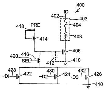
Figure 9 is a schematic diagram illustrating one embodiment of an
identification cell 400 in one embodiment of a printhead die 40. The printhead
die 40 includes a plurality of identification cells electrically coupled to
one
identification line 402. The identification line 402 receives an
identification
signal ID and provides the identification signal ID to the identification
cells.
Each of the identification cells is similar to identification cell 400.
The identification cell 400 includes a memory element, indicated at 403.
The memory element 403 stores one bit of information. In one embodiment,
memory element 403 is a fuse represented by fuse element 404 and fuse
resistance 408. In other embodiments, memory element 403 can be another
suitable memory element, for example an anti-fuse that provides a high
resistive
state before being programmed and a low resistive state after being
programmed with a program signal.
The identification cell 400 includes a drive switch 406 electrically coupled
to memory element 403. In one embodiment, drive switch 406 is a FET
including a drain-source path electrically coupled at one end to one terminal
of
memory element 403 and at the other end to a reference 410, such as ground.
The other terminal of memory element 403 is electrically coupled to
identification line 402. The identification line 402 receives identification
signal
ID and provides identification signal ID to memory element 403. The
identification signal ID, including the program signal and the read signal,
can be
CA 02563730 2006-10-18
WO 2005/105451 PCT/US2005/011395
24
conducted through memory element 403 if drive switch 406 is turned on
(conducting). This allows for only specific identification cells 400 on a
single
identification line 402 to respond to read and programming signals on the
identification line 402, while other identification cells on the same
identification
line 402 do not respond to the read and programming signals.
The gate of drive switch 406 forms storage node capacitance 412, which
functions as a memory to store charge pursuant to the sequential activation of
pre-charge transistor 414 and select transistor 416. The drain-source path and
gate of pre-charge transistor 414 are electrically coupled to pre-charge line
418
that receives a pre-charge signal PRE. In one embodiment, pre-charge line 418
is electrically connected to one of the pre-charge lines 210, (Figure 7).
The gate of drive switch 406 is a control input that is electrically coupled
to the drain-source path of pre-charge transistor 414 and the drain-source
path
of select transistor 416. The gate of select transistor 416 is electrically
coupled
to select line 420 that receives a select signal SEL. In one embodiment,
select
line 420 is electrically connected to one of the select lines 212, (Figure 7).
The
storage node capacitance 412 is shown in dashed lines, as it is part of drive
switch 406. Alternatively, a capacitor separate from drive switch 406 can be
used to store charge.
A first transistor 422, a second transistor 424 and a third transistor 426
include drain-source paths that are electrically coupled in parallel. The
parallel
combination of first transistor 422, second transistor 424 and third
transistor 426
is electrically coupled between the drain-source path of select transistor 416
and
reference 410. The serial circuit including select transistor 416 coupled to
the
parallel combination of first transistor 422, second transistor 424 and third
transistor 426 is electrically coupled across node capacitance 412 of drive
switch 406. The gate of first transistor 422 is electrically coupled to data
line
428 that receives data signal -D1. The gate of second transistor 424 is
electrically coupled to data line 430 that receives data signal -D2 and the
gate
of third transistor 426 is electrically coupled to data line 432 that receives
data
signal -D3. The data signals -D1, -D2 and -D3 are active low as indicated by
the tilda (-) preceding each signal name. The drive switch 406 including node
CA 02563730 2006-10-18
WO 2005/105451 PCT/US2005/011395
capacitance 412, pre-charge transistor 414, select transistor 416, first
transistor
422, second transistor 424 and third transistor 426 form a dynamic memory
circuit or cell.
In one embodiment, data signals -D1, -D2 and -D3 provided to
5 identification cell 400 are data signals -D1, -D2 and -D3 provided on data
lines
208a-208c to all fire groups 202a-202f (Figure 7). Also, in one embodiment,
pre-charge signal PRE is pre-charge signal PRE1 provided on pre-charge line
210a to fire group 202a. In addition, in one embodiment, select signal SEL is
select signal SEL1 provided on select line 212a to fire group 202a.
10 To program memory element 403, identification cell 400 receives
enabling signaling, including pre-charge signal PRE, select signal SEL and
data
signals -D1, -D2 and -D3 to turn on drive switch 406. Identification line 402
provides the program signal in the identification signal ID to memory element
403. The program signal provides a current through memory element 403 to the
15 conducting drive switch 406 and reference 410. The program signal changes
the state of memory element 403 from the low resistive state to the high
resistive state. In one embodiment, the program signal is a fourteen volt
signal
provided for one micro-second.
To read the state of memory element 403, identification cell 400 receives
20 enabling signaling, including pre-charge signal PRE, select signal SEL and
data
signals -D1, -D2 and - D3 to turn on drive switch 405. Identification line 402
provides the read signal in the identification signal ID to memory element
403.
The read signal provides a current through memory element 403 to the
conducting drive switch 406 and reference 410. The voltage on identification
25 line 402 is determined to determine the resistive state of memory element
403.
In one embodiment, memory element 403 is determined to be in the high
resistive state if the resistance is greater than about 1000 ohms and in the
low
resistive state if the resistance is less than about 400 ohms.
In operation, node capacitance 412 is pre-charged through pre-charge
transistor 414 by providing a high level voltage pulse in pre-charge signal
PRE
on pre-charge line 418. After charging node capacitance 412, a data signal -D1
is provided on data line 428 to set the on/off state of first transistor 422,
data
CA 02563730 2006-10-18
WO 2005/105451 PCT/US2005/011395
26
signal -D2 is provided on data line 430 to set the on/off state of second
transistor 424 and data signal -D3 is provided on data line 432 to set the
on/off
state of third transistor 426. After the high level voltage pulse in pre-
charge
signal PRE and after pre-charge signal PRE returns to a low voltage level, a
high level voltage pulse is provided in select signal SEL on select line 420
to
turn on select transistor 416. Node capacitance 412 is actively discharged if
at
least one of the first, second, and third transistors 422, 424 and 426 is
turned on
by one of the data signals -D1,-D2 or -D3, respectively. Alternatively, node
capacitance 412 remains charged if first transistor 422, second transistor 424
and third transistor 426 are turned off by data signals -D1, -D2 or -D3. A
charged node capacitance 412 turns on drive switch 406 and memory element
403 can be programmed with a program signal and read with a read signal.
In one embodiment, the program signal and/or read signal are initiated
while node capacitance 412 is actively discharged through select transistor
416
and at least one of the first, second and third transistors 422, 424 and 426.
The
high level voltage pulse in select signal SEL overlaps the start of the
program
signal and/or read signal on identification line 402. Also, valid data signals
-D1,
-D2 and -D3 overlap the start of the program signal and/or read signal on
identification line 402.
In one embodiment, node capacitance 412 is actively discharged through
select transistor 416 and at least one of the first, second and third
transistors
422, 424 and 426 during the entire program signal and/or the entire read
signal.
The high level voltage pulse in select signal SEL overlaps the entire program
signal and/or read signal on identification line 402. Also, valid data signals
-D1,
-D2 and -D3 overlap the entire program signal and/or read signal on
identification line 402. Actively discharging node capacitance 412 during at
least the rise time of the program signal and/or the rise time of the read
signal
prevents node capacitance 412 from being inadvertently charged to turn on a
drive switch 406.
Identification cell 400 is selected and addressed for programming and
reading if data signals -D1, -D2 and -D3 are low and node capacitance 412
remains charged to turn on drive switch 406. Identification cell 400 is not
CA 02563730 2006-10-18
WO 2005/105451 PCT/US2005/011395
27
selected for programming or reading if at least one of the data signals -D1, -
D2
and -D3 are high and node capacitance 412 discharges to turn off drive switch
406. The first, second and third transistors 422, 424 and 426 comprise a
decoder that controls the voltage level on node capacitance 412.
In one embodiment, data signals -D1, -D2 ... -D8 provided on data lines
208a-208h to fire groups 202a-202f (shown in Figure 7) are provided to
identification cells 400, in printhead die 40. With three of eight data
signals
-D1, -D2 ... -D8 selecting each identification cell 400 in a plurality of
identification cells, up to fifty six different identification cells can be
selected by
the eight data signals -D1, -D2 ... -D8. The combination of the eight data
signals -D1, -D2 ... -D8, in reverse order, that, in one embodiment, are
utilized
to activate each individual identification cell 400, are shown in the
following
Table I:
TABLE I
I DCel l:-D8--D 1 I DCell:-D8--D 1 I DCeI I:-D8---D 1 I DCell:-D8--D 1
1:11111000 15:01110110 29:10110101 43:01101011
2:11110100 16:11001110 30:01110101 44:10011011
3:11101100 17:10101110 31:11001101 45:01011011
4:11011100 18:01101110 32:10101101 46:00111011
5:10111100 19:10011110 33:01101101 47:11000111
6:01111100 20:01011110 34:10011101 48:10100111
7:11110010 21:00111110 35:01011101 49:01100111
8:11101010 22:11110001 36:00111101 50:10010111
9:11011010 23:11101001 37:11100011 51:01010111
10:10111010 24:11011001 38:11010011 52:00110111
11:01111010 25:10111001 39:10110011 53:10001111
12:11100110 26:01111001 40:01110011 54:01001111
13:11010110 27:11100101 41:11001011 55:00101111
14:10110110 28:11010101 42:10101011 56:00011111
CA 02563730 2006-10-18
WO 2005/105451 PCT/US2005/011395
28
As can be seen from Table 1, each identification cell 400 can be
individually enabled, and thereby can be programmed on an individual basis.
Also, since the identification cells 400 can be read individually, the
combinations
utilized to store data are greatly increased. For example, a single
identification
cell 400 may be utilized in multiple combinations that each represents
different
information.
In one embodiment, printhead die 40 includes a pre-charge line, a select
line, eight data lines, and an identification line coupled to fifty six
identification
cells. These eleven lines are used to control fifty six identification bits or
about
5.1 identification cell bits per control line. In other embodiments, any
suitable
number of data signals can be provided to the identification cells. Also, in
other
embodiments, each identification cell can be configured to respond to any
suitable number of data signals, such as two or four or more data signals. The
uses for identification cells 400 can be similar to uses described for
identification
cells in this specification.
A plurality of identification cells, similar to identification cell 400, in an
example embodiment of printhead die 40, store identification information
indicating features of or other information about printhead die 40. A printer
employing such a printhead having identification cells can use this
identification
information to optimize printing quality in a variety of printing
applications. Also,
the printer can use this identification information for marketing purposes,
such
as regional marketing and original equipment manufacturer (OEM) marketing.
In one embodiment, selected identification cells store identification
information indicating a thermal sense resistance value as determined at a
selected temperature, such as 32 degrees centigrade. In this embodiment, a
printhead includes a thermal sense resistor (TSR) that is read to provide a
TSR
value. The TSR is read and the obtained value is compared to the thermal
sense resistance value stored in the identification cells to determine the
temperature of the printhead. Printers can use this TSR information to
optimize
printing quality.
In one embodiment, selected identification cells store identification
information indicating a printhead uniqueness number. The printer can use the
CA 02563730 2006-10-18
WO 2005/105451 PCT/US2005/011395
29
printhead uniqueness number, along with other identification information, to
identify and properly respond to the printhead.
In one embodiment, selected identification cells store identification
information indicating an ink drop weight for a printhead. In one embodiment,
the ink drop weight is indicated as an ink drop weight delta value or change
from a selected nominal ink drop weight value.
In some embodiments, identification cells store identification information
not only about the printhead die, but also about the inkjet cartridge or pen
in
which the printhead die is inserted. For example, in one embodiment, selected
identification cells store identification information indicating an out of ink
detection level for an inkjet cartridge. In one embodiment, a printer accounts
for
the drop weight values stored in selected identification cells and the out of
ink
detection level information stored in other selected identification cells to
determine actual out of ink detection levels.
In one embodiment, one or more selected identification cells store
identification information indicating which company sells a fluid ejection
device.
For example, one or more selected identification cells can store
identification
information indicating that the fluid ejection device is sold under a certain
company's brand name or not sold under that certain company's brand name.
In one embodiment, selected identification cells store identification
indicating a marketing region for the fluid ejection device. In one
embodiment,
selected identification cells store identification information indicating the
seller of
an OEM fluid ejection device. In one embodiment, selected identification cells
in
a printhead store identification indicating whether an OEM printer is
unlocked.
For example, the OEM printer can respond to the OEM unlocked information to
unlock an OEM printer, such that the OEM printer can accept OEM printheads
sold by a given company or group of companies and printheads sold by
companies other than the given company or group of companies, such as the
actual original manufacturer company.
In one embodiment, selected identification cells store identification
information indicating the product type and product revision of a fluid
ejection
device. The product type and product revision can be used by a printer to
CA 02563730 2010-06-15
ascertain physical characteristics about a printhead. In one embodiment,
product
revision physical characteristics, such as spacing between nozzle columns,
that may
change in future products are stored in selected identification cells of a
printhead. In
this embodiment, the product revision physical characteristic information can
be used
5 by the printer to adjust for the physical characteristic changes between
product
revisions.
It should be noted that while Figure 9 discloses utilizing a single
identification
line 402 that is coupled to each of the identification cells 400, e.g. 56
identification
cells, more than one identification line 400 may be utilized. Also, the number
of
10 identification cells that are provided may be more or less than 56
depending of
factors such as the size of the die, the operating parameters of the fluid
ejection
device, or other considerations. Also, the number of identification cells that
are
encoded with information may be less than the total number of identification
cells on
the die.
15 Also, the memory element 403 may be encoded with multiple bits of
information. In such an instance, different ranges of resistance may be
utilized to
represent each bit. An example of a system and method for encoding a memory
element with multiple bits of information is depicted and disclosed in U.S.
Patent No.
7,108,357 to Rice et at.
20 Figure 10 is a diagram illustrating one embodiment of a portion of a
printhead
die 40. The printhead die 40 includes an identification signal input pad 702,
a data
line input pad 704 and a fire line input pad 706. The identification signal
input pad
702, data line input pad 704 and fire line input pad 706 are formed as part of
the
second metal layer of printhead die 40. The identification signal input pad
702 is
25 electrically coupled to identification line 708 that is electrically
coupled to
identification cells such as identification cell 400, or other identification
elements, in
printhead die 40. The data line input pad 704 is electrically coupled to data
line 710
that is electrically coupled to firing cells 120 in printhead die 40. The fire
line input
pad 706 is electrically coupled to fire line 712 that is electrically coupled
to firing cells
30 120 in printhead die 40.
CA 02563730 2006-10-18
WO 2005/105451 PCT/US2005/011395
31
The identification line 708 includes second metal layer portions 708a-
708c and first metal layer portions 708d and 708e. The second metal layer is
isolated from the first metal layer by an isolation layer. Contact is made
between second metal layer portions 708a-708c and first metal layer portions
708d and 708e through vias 714a-714d. Second metal layer portion 708a is
electrically coupled to first metal layer portion 708d through via 714a. The
first
metal layer portion 708d is electrically coupled to second metal layer portion
708b through via 714b. The second metal layer portion 708b is electrically
coupled to first metal layer portion 708e through via 714c, and first metal
layer
portion 708e is electrically coupled to second metal'layer portion 708c
through
via 714d.
The data line 710 is formed as part of the second metal layer and
disposed over first metal layer portion 708e of identification line 708. Fire
line
712 is formed as part of the second metal layer and disposed over first metal
layer portion 708d of identification line 708. The first metal layer is
isolated from
the second metal layer by the isolation layer and identification line 708 is
isolated from data line 710 and from fire line 712. The data line 710 receives
data signal DATA and provides data signal DATA to firing cells 120. Fire line
712 receives fire signal FIRE and provides fire signal FIRE to firing cells
120 in
printhead die 40.
The second metal layer portion 708a includes an elongated finger
portion, indicated at 720, that is situated next to fire line input pad 706,
and
second metal layer portion 708b includes an elongated finger portion,
indicated
at 722, that is situated next to data line input pad 704. Identification line
708
receives identification signal ID and provides identification signal ID to
identification cells, such as identification cell 400, or other identification
elements in printhead die 40. Also, identification line 708 receives a short
detection signal in identification signal ID. The short detection signal is
used to
detect fluid short circuits, such as ink short circuits, between data line
input pad
704 and finger portion 722, and between fire line input pad 706 and finger
portion 720.
CA 02563730 2010-06-15
32
To detect a short circuit between data line input pad 704 and finger portion
722, probes are positioned on identification signal input pad 702 and data
line input
pad 704. The short detection signal is provided to identification signal input
pad 702
and ground is provided at data line input pad 704. A short circuit is detected
as a low
voltage level on identification signal input pad 702. To detect a short
circuit between
fire line input pad 706 and finger portion 720, probes are positioned on
identification
signal input pad 702 and fire line input pad 706. The short detection signal
is
provided to identification signal input pad 702 and ground is provided at fire
line input
pad 704. A short circuit is detected as a low voltage level on identification
signal
input pad 702. This short circuit detection test can be used for each input
pad that
has identification line 708 situated next to it. The short circuit detection
test is used
as a substitute for detecting ink shorts between input pads, such as data line
input
pad 704 and fire line input pad 706. In one embodiment, signal input pads 702,
704
and 706 have a pad width WP of 125 microns and between pad spacing WBP of 50
microns. The spacing between finger portion 722 and data line input pad 704 at
WIDS is 10 microns, and the spacing between finger portion 720 and fire line
input
pad 706 is 10 microns.
Examples of other identification elements or identification cells that may be
utilized with layouts of identification signal input pad 702, data line input
pad 704 and
fire line input pad 706 are depicted and disclosed in U.S. Patent No.
6,966,622 to
Dodd and U.S. Patent No. 5,363,134.
Figure 11 is a flow chart illustrating one embodiment of a manufacturing
process employing selected identification cells in certain embodiments of
printhead
die 40. In certain embodiments of printhead die 40, the operating speed is
dependent on the time it takes to charge and discharge internal circuit nodes.
These
charge and discharge times are dependent on the speed of the silicon and may
vary
from one printhead die 40 to the next due to slight differences in the
properties of the
substrate from which the printhead die 40 is formed. By characterizing the
speed of
a printhead die 40 and encoding the speed on the printhead die 40, after
testing,
applications can use some
CA 02563730 2006-10-18
WO 2005/105451 PCT/US2005/011395
33
printhead die 40 in higher performance applications and other printhead die 40
in lower performance applications.
In a printhead die 40 including pre-charged firing cells 120 in a firing cell
array similar to firing cell array 200 illustrated in Figure 7, fire signals
FIREI,
FIRE 2 ... FIRE6 include energy pulses that overlap as illustrated in the
timing
diagram of Figure 8. The operating speed of printhead die 40 may be
dependent on the time it takes to charge and discharge address lines 144 and
146 for selecting and deselecting firing cells 120, the time it takes to
discharge
node capacitance 126 through select transistor 130 before an energy pulse is
provided in fire signal FIRE, and the time it takes to precharge node
capacitance
126.
At 800, timing parameters of printhead die 40 that include pre-charged
firing cells 120 in firing cell arrays similar to firing cell array 200 are
characterized in testing of the printhead die 40. In each characterized
printhead
die 40, the characterized timing parameters include charge and discharge times
of one or more address lines, such as address lines 144 and 146. Also, in each
characterized printhead die 40, the characterized timing parameters include
the
discharge time of one or more node capacitances 126. The timing
characteristics of each characterized printhead die 40 are categorized into a
designated speed category.
At 802, the designated speed category of a characterized printhead die
40 is programmed into selected identification cells in the characterized
printhead
die 40. The identification cells in the characterized printhead die 40 are
similar
to identification cell 400 illustrated in Figure 9. The selected
identification cells
400 in each characterized printhead die 40 can be read at 804 and the
printhead die 40 are sorted based on the speed performance category.
At 806, printhead die 40 that are categorized into higher speed
performance categories are implemented in printers having higher performance
print modes. At 808, printhead die 40 that are categorized into lower speed
performance categories are implemented in lower performance printers, such as
lower cost printers that do not include the higher performance print modes of
the
higher performance printers.
CA 02563730 2006-10-18
WO 2005/105451 PCT/US2005/011395
34
The operating speed of other embodiments of printhead die 40 may also
be dependent on the time it takes to charge and discharge internal circuit
nodes. For example, in one embodiment where dynamic firing cells are first
discharged, the operating time may be dependent on the time it takes to charge
the gate of the drive switch, instead of the time it takes to discharge the
gate of
the drive switch.
Although specific embodiments have been illustrated and described
herein, it will be appreciated by those of ordinary skill in the art that a
variety of
alternate and/or equivalent implementations may be substituted for the
specific
embodiments shown and described without departing from the scope of the
present invention. This application is intended to cover any adaptations or
variations of the specific embodiments discussed herein. Therefore, it is
intended that this invention be limited only by the claims and the equivalents
thereof.
What is Claimed is: