Note: Descriptions are shown in the official language in which they were submitted.
CA 02563953 2006-10-26
WO 2005/112744 PCT/US2005/017723
EMBEDDED BIO-SENSOR SYSTEM
CROSS-REFERENCE TO RELATED APPLICATIONS
Not Applicable
STATEMENT RE: FEDER.ALLY SPONSORED RESEARCH/DEVELOPMENT
Not Applicable
BACKGROUND OF THE INVENTION
The present invention relates to sensor devices and, more particularly, to an
bio-sensor system configured for wirelessly transmitting data to a remote
transponder
from an on-chip transponder having a sensor and which is implantable in a
patient.
The bio-sensor system is specifically adapted to apply a stable and precise
voltage to
an electrode system of the sensor such that glucose concentration levels of
the patient
may be accurately measured.
The blood glucose concentration level of a patient is normally controlled by
the pancreas. However, for patients suffering from diabetes, the pancreas does
not
properly regulate the production of insulin needed to metabolize food into
energy for
the individual. For diabetic patients, glucose levels must be checked or
monitored
several times throughout the day so that insulin may be periodically
administered in
order to maintain the glucose concentration at a normal level. In one popular
method,
the glucose level is monitored by first obtaining a sample of blood from
finger-
pricking. The glucose level of the blood sample is then placed on a glucose
measurement strip and a subsequent chemical reaction produces a color change
that
may be compared to a reference chart. In this manner, the reaction of the
blood
sample with the glucose measurement strip provides an indication as to whether
the
glucose level is abnormally low or high such that the diabetic patient may
administer
the proper amount of insulin in order to maintain the glucose concentration
within a
predetermined range. Such administration of insulin is typically performed by
way of
self-injection with a syringe.
Unfortunately, the finger-pricking method of glucose testing is uncomfortable
as both the blood-pricking and the insulin injections are painful and time-
consuming
such that many diabetic patients are reluctant to check their glucose levels
at regular
CA 02563953 2006-10-26
WO 2005/112744 PCT/US2005/017723
2
intervals throughout the day. Unfortunately, glucose levels often fluctuate
throughout
the day. Therefore, even diabetic patients who are otherwise consistent in
checking
their glucose levels at regular intervals throughout the day may be unaware of
periods
wherein their glucose levels are dangerously low or high. Furthermore, the
finger-
pricking method is dependent on patient skill for accurate testing such that
the patient
may rely on erroneous data in deterinining the dosage level of insulin.
Finally, self-
monitoring of glucose levels imposes a significant burden on less capable
individuals
such as the young, the elderly and the mentally-challenged.
At the time of this writing, it is estimated that 17 million people in the
United
States, or about six percent of the population, have diabetes. Due in part to
dietary
habits and an increasingly sedentary lifestyle, particularly among children,
diabetes is
expected to increase at the rate of about 7 percent every year such that the
disease is
predicted to eventually reach epidemic proportions. In addition, the current
cost of
diabetes in the United States alone is estimated at over $120 billion with the
total U.S.
sales of the glucose measuring strips alone estimated at about $2 billion.
Thus, there
is a demand for continuous, reliable and low-cost monitoring of glucose levels
of
diabetic patients due to the increasing number of people diagnosed with
diabetes.
Included in the prior art are several implantable devices have been developed
in an effort to provide a system for continuous and reliable glucose
monitoring. In
such implantable devices, an electrochemical sensor is embedded beneath the
skin of
the patient. The electrochemical sensor detects the glucose concentration
level and
transmits signals representative of the glucose concentration level to a
receiving
device. Unfortunately, such implantable devices suffer from several
deficiencies.
One such deficiency is that implantable devices may expend a substantial
amount of
power in sensing and processing bio-signals. The power requirement for such
devices
necessitates the use of large batteries in order to prolong the useful life.
Unfortunately, implantable devices having batteries as the power source may
require
periodic surgeries for replacement of the batteries when the capacity drops
below a
minimum level.
Furthermore, some batteries contain materials that may present a risk of harm
to the patient due to toxic substances or chemical within the battery that may
leak into
the patient after implantation. Also, due to the relatively limited power
capacity of
batteries, the range of functions that may be performed by the implantable
device may
CA 02563953 2006-10-26
WO 2005/112744 PCT/US2005/017723
3
be somewhat limited. Finally, it may be desirable to monitor multiple
physiological
parameters in addition to glucose concentration levels. In such cases, the
implantable
device may require multiple sensors wherein each sensor simultaneously
monitors a
different physiological parameter of the patient. For example, in addition to
monitoring glucose concentration levels, the temperature and heart rate of the
patient
may also be monitored. Such an implantable device having multiple sensors may
consume more power than can be supplied by a battery that is miniaturized for
use in
an implantable device.
One implantable device in the prior art overcomes the above noted deficiency
associated with large power requirements by providing a bio-sensor system that
is
passively powered such that the operating life of the bio-sensor is
theoretically
unlimited. As understood, the passively powered bio-sensor system includes at
least
one sensor that is implanted in a patient. The implanted sensor monitors
physiological conditions of the patient. An implanted passive transponder
receives
the sensor signals from the sensor, digitizes the sensor signals and transmits
the
digitized sensor signal out of the patient's body when subjected to an
interrogation
signal from a remote interrogator. The interrogator also energizes the
implanted
transponder such that the bio-sensor system may be passively powered. In this
manner, the passively powered bio-sensor system requires no batteries such
that it
essentially has an unlimited operating life.
Another deficiency of implantable devices pertains to electrochemical sensors
that are utilized therein to measure glucose concentration levels in the
patient's blood.
Such sensors typically use an amperometric detection method wherein oxidation
or
reduction of a compound is measured at a working electrode in order to
determine
substance concentration levels. A potentiostat is used to apply a constant
potential or
excitation voltage to the working electrode witli respect to a reference
electrode. In
measuring glucose concentration levels in the blood, glucose oxidase (GOX) is
typically used as a catalyst to oxidize glucose and form gluconic acid,
leaving behind
two electrons and two protons and reducing the GOX. Oxygen that is dissolved
in the
patient's blood then reacts with GOX by accepting the two electrons and two
protons
to form hydrogen peroxide (H202) and regenerating oxidized GOX.
The cycle repeats as the regenerated GOX reacts once again with glucose.
The consumption of 02 or the formation of H202 is subsequently measured at the
CA 02563953 2006-10-26
WO 2005/112744 PCT/US2005/017723
4
working electrode which is typically a platinum electrode. As oxidation occurs
at the
working electrode, reduction also occurs at the reference electrode which is
typically
a silver/silver chloride electrode. The more oxygen that is consumed, the
greater the
amount of glucose in the patient's blood. In the same reaction, the rate at
which H202
is produced is also indicative of the glucose concentration level in the
patient's blood.
Because the potentiostat controls the voltage difference between the working
electrode and the reference electrode, the accuracy with which the sensor
measures
glucose concentration levels is dependent on the accuracy with which the
voltage is
applied. If the voltage that is applied to the sensor is excessive, the silver
or silver
cllloride reference electrode may be excessively consumed such that the
reference
electrode may become damaged. Furthermore, erroneous measurements of glucose
concentration levels may result such that the ability of the patient to
administer insulin
in order to correct for abnormalities in glucose concentration levels may be
compromised
In an attempt to overcome the above-described deficiency associated with
two-electrode electrochemical sensors, three-electrode electrochemical sensors
have
been developed wherein an auxiliary electrode is included with the working
electrode
and the reference electrode. The inclusion of the auxiliary electrode is
understood to
reduce the consumption of silver and silver chloride by reducing the magnitude
of
current flowing through the reference electrode, thereby stabilizing the
electrode
potential. Unfortunately, such three-electrode electrochemical sensors of the
type
describe above add complexity and cost to the bio-sensor system due to the
increased
difficulty in manufacturing and operating such electrochemical sensors.
As can be seen, there is a need for an implantable bio-sensor system that
overcomes the above-described deficiencies associated with the stability of
the
reference electrode potential with respect to the working electrode. More
specifically,
there exists a need in the art for an implantable bio-sensor system that
provides a
stable and accurate voltage to the electrochemical sensor in order to improve
the
accuracy with which glucose concentration levels may be measured. In
combination
with the power requirements, there is also a need in the art for an
implantable bio-
sensor system that enables the simultaneous and selective monitoring of
multiple
physiological parameters of the patient through the use of multiple bio-
sensors
included with the implantable device. Furthermore, there exists a need in the
art for
CA 02563953 2006-10-26
WO 2005/112744 PCT/US2005/017723
an implantable bio-sensor system which allows full-duplex operation such that
requests for data (i.e., physiological parameters of the patient) and
transmission of
such data can be simultaneously performed. Finally, there is a need in the art
for an
implantable bio-sensor system that enables continuous readout of the data at a
remote
5 device.
BRIEF SUMMARY OF THE INVENTION
Provided is a telemetric bio-sensor system which utilizes radio frequency
identification (RFID) technology and which includes a remote transponder that
is in
wireless communication with a passively powered on-chip transponder. The bio-
sensor system is specifically adapted to provide a substantially stable and
precise
voltage to a sensor assembly that is included with an implantable on-chip
transponder.
The remote transponder is placed within a predetermined distance of the on-
chip
transponder in order to supply power to and request telemetry data from the on-
chip
transponder. The remote transponder is also configured to remotely receive
data
representative of a physiological parameter of the patient as well as
identification data
and may enable readout of one or more of the physiological parameters that are
measured, processed and transmitted by the on-chip transponder upon request by
the
remote transponder.
Importantly, the power receiver supplies a substantially non-deviating sensor
reference voltage to the sensor in order to enhance the accuracy with which
the
physiological parameter is measured. The precision and stability of the sensor
reference voltage (i.e., the sensor power) is enhanced by the specific circuit
architecture of the glucose sensor. The application of the substantially
stable voltage
to the sensor assembly allows ' for relatively accurate measurement of the
physiological parameter of the patient such as measurement of a glucose
concentration level by a glucose sensor. The technique of generating the
stable and
precise voltage may be applied to a 2-pin glucose sensor as well as to a 3-pin
glucose
sensor without the use of a microprocessor such that cost and power
consumption of
the on-chip transponder may be reduced. Advantageously, the stability and
accuracy
of the sensor reference voltage is achieved without the use of a
microprocessor to
reduce power consumption of the on-chip transponder as well as reduce overall
costs
of the bio-sensor system.
CA 02563953 2006-10-26
WO 2005/112744 PCT/US2005/017723
6
The on-chip transponder includes the sensor assembly having the sensor which
may be the 2-pin or 3-pin glucose sensor. However, any other sensor may be
used
with the on-chip transponder. Components of the on-chip transponder may
include:
the sensor, a power receiver, an analog-to-digital (A/D) assembly, a data
processor
and an RF transmitter which may preferably be interconnected using
conventional
integrated circuit technology such that the on-chip transponder may be
packaged into
a sufficiently small size for implantation into a patient. An RF receiver may
also be
included with the on-chip transponder to allow for selection among a plurality
of
sensors and to allow for full-duplexing, which enables continuous and/or
simultaneous two-way wireless communication between the remote transponder and
the on-chip transponder.
The remote transponder emits a scanner signal that is received by a power
receiver of the on-chip transponder. The power receiver converts the scanner
signal
to a power signal to power the A/D assembly, a data processor and an RF
transmitter.
The A/D assembly converts the physiological parameter contained in an analog
electrical signal coming from the sensor into digital format in a digital
signal. The
A/D assembly may also add a unique identification code to the digital signal
to
identify the particular sensor from which the sensor signal originated.
The data processor receives the digital signal from the A/D assembly and
filters, amplifies and/or encodes the digital signal to generate a processed
data signal.
The data processor may also gate the data signal to determine when to transmit
the
data signal and may also sum the data signal with other data (i.e., from other
sensors).
The RF transmitter iinpresses (i.e., modulates) the data signal onto a radio
carrier of a
desired frequency, amplifies the modulated carrier and sends it to an antenna
for
radiation to the remote transponder.
BRIEF DESCRIPTION OF THE DRAWINGS
These as well as other features of the present invention will become more
apparent upon reference to the drawings wherein:
Figure la is a block diagram of a sensor assembly and an on-chip transponder
of an implantable bio-sensor system of the present invention in an embodiment
enabling simplex operation wherein the content and duration of a signal
transmitted
by the on-chip transponder is pre-programmed;
CA 02563953 2006-10-26
WO 2005/112744 PCT/US2005/017723
7
Figure lb is a block diagram of the sensor assembly and the on-chip
transponder of the bio-sensor system in an embodiment enabling duplex
operation
wherein the duration and content of signals transmitted by the on-chip
transponder to
a remote transponder, and vice versa, is selectable;
Figure 2 is a block diagram of a remote transponder of the implantable bio-
sensor system;
Figure 3 is a block diagram of a data processor that may be included with the
on-chip transponder;
Figure 4 is a block diagram of a radio frequency (RF) transmitter that may be
included with the on-chip transponder;
Figure 5a is a block diagram of an analog-to-digital (A/D) assembly as may be
included with the on-chip transponder for the embodiment of the bio-sensor
system
configured to receive a single one of the sensor signals;
Figure 5b is a block diagram of the A/D assembly as may be included with the
on-chip transponder for the embodiment of the bio-sensor system that may
include a
switch for selecting a sensor signal sent from multiple sensors;
Figure 6 is a block diagram of a power receiver that may be included with the
on-chip transponder;
Figure 7 is a block diagram of an RF receiver that may be included with the
on-chip transponder;
Figure 8a is a schematic representation of a 2-pin glucose sensor as may be
incorporated into the sensor assembly; and
Figure 8b is a schematic representation of a 3-pin glucose sensor as may be
incorporated into the sensor assembly.
DETAILED DESCRIPTION OF THE INVENTION
Referring now to the drawings wherein the showings are for purposes of
illustrating various aspects of the invention and not for purposes of limiting
the same,
provided is a uniquely configured telemetric bio-sensor system 10 which
utilized
radio frequency identification (RFID) technology and which includes a remote
transponder 800 that is in wireless communication with a passively powered on-
chip
transponder 100. The bio-sensor system 10 is specifically adapted to provide a
substantially stable and precise voltage to a sensor assembly 200 that is
included with
CA 02563953 2006-10-26
WO 2005/112744 PCT/US2005/017723
8
the on-chip transponder 100. The on-chip transponder 100 is implantable into a
host
such as a human patient.
The remote transponder 800, which may be a compact handheld device, may
be manually placed within a predetermined distance (e.g., within several feet)
of the
on-chip transponder 100 in order to supply power to and request telemetry data
from
the on-chip transponder 100. The remote transponder 800 may alternatively be
fixedly mounted and may be configured to automatically transmit power and
telemetry request data to the patient and, hence, the on-chip transponder 100
when the
patient moves within the predetermined distance to the remote transponder 800.
Regardless of whether it is handheld, fixedly mounted or otherwise supported,
the
remote transponder 800 is configured to remotely receive data representative
of a
physiological parameter of the patient as well as identification data such
that the data
may be stored or displayed.
Importantly, the application of the substantially stable voltage to the sensor
assembly 200 allows for relatively accurate measurement of the physiological
parameter of the patient such as measurement of a glucose concentration level
by a
glucose sensor 210. As will be demonstrated below, the technique of generating
the
stable and precise voltage may be applied to a 2-pin glucose sensor 210 as
well as to a
3-pin glucose sensor 210. Importantly, the bio-sensor system 10 provides the
stable
and precise voltage to the sensor assembly 200 without the use of a
microprocessor
such that cost and power consumption of the on-chip transponder 100 may be
reduced.
In its broadest sense, the bio-sensor system 10 and operational method of use
thereof comprises the implantable on-chip transponder 100 and the remote
transponder 800 in wireless communication with one another. As mentioned
above,
the sensor assembly 200 is connected to or integral with the on-chip
transponder 100
and may be implanted in the patient with the on-chip transponder 100. The bio-
sensor
system 10 is configured such that the remote transponder 800 may enable
readout of
one or more of the physiological parameters that are measured, processed and
transmitted by the on-chip transponder 100 upon request by the remote
transponder
800. The bio-sensor system 10 may be configured to operate in simplex mode as
shown in Fig. 1 a.
CA 02563953 2006-10-26
WO 2005/112744 PCT/US2005/017723
9
Alternatively, the bio-sensor system 10 may be configured to operate in
duplex mode as shown in Fig. lb wherein the on-chip transponder 100
additionally
includes an intelligent radio frequency (RF) receiver. When provided with the
RF
receiver 700, the bio-sensor system 10 enables features such as selection
between
multiple sensors 210 and/or continuous readout of data (e.g., physiological
parameters
of the patient) in addition to readout of identification data which may be
correlated to
a patient database containing information regarding the patient's identity as
well as
information regarding the patient's age, weight, medical history, etc.
Referring more particularly now to Figs. la and 1b, shown are block diagrams
of the sensor assembly 200 as connected to the on-chip transponder 100 of the
bio-
sensor system 10 for respective embodiments enabling simplex and duplex
operation.
The on-chip transponder 100 includes the sensor assembly 200 having the sensor
210.
The sensor 210 may be configured as the 2-pin glucose sensor 210 or as 3-pin
glucose
sensor 210 as was mentioned above. However, any other sensor may be used with
the
on-chip transponder 100. For example, the sensor 210 may be configured as at
least
one of the following: a pressure transducer, a blood sugar sensor, a blood
oxygen
sensor, a heart rate monitor, a respiratory rate sensor, etc. In this regard,
the sensor
210 may be configured as any type of sensor for measuring, monitoring or
detecting
any type of physiological parameter of the patient.
Shown in Fig. 2 is a block diagram of the remote transponder 800. The
remote transponder 800 is configured to wirelessly request data regarding the
physiological parameter by transmitting a scanner signal 882 to the on-chip
transponder 100. The remote transponder 800 is also configured to receive a
data
signal 462 representative of the physiological parameter from the on-chip
transponder
100. In the same manner, the on-chip transponder 100 is configured to
communicate
with the remote transponder 800 and receive the scanner signal 882 and
transmit the
data signal 462 therefrom once the remote transponder 800 and on-chip
transponder
100 are within sufficiently close proximity to one another to enable wireless
communication therebetween.
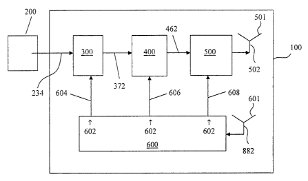
Components of the on-chip transponder 100 for the embodiment of the bio-
sensor system 10 enabling simplex operation include: the sensor 210, a power
receiver 600, an analog-to-digital (A/D) assembly 300, a data processor 400
and an
RF transmitter 500, as shown in Fig. la. For embodiments of the bio-sensor
system
CA 02563953 2006-10-26
WO 2005/112744 PCT/US2005/017723
10 enabling duplex operation, the RF receiver 700 is included with the on-chip
transponder 100, as shown in Fig. lb. Each of the components of the on-chip
transponder 100 may be electrically interconnected via conventional conductive
wiring. However, electrical connections may preferably be provided using
5 conventional integrated circuit technology such that the on-chip transponder
100 may
be packaged into a sufficiently small size for implantation into the patient.
The sensor 210 is configured to generate a sensor signal 234 representative of
the physiological parameter of the patient and is made up of a positive signal
and a
negative signal transmitted in parallel and sent from the sensor 210 to the
A/D
10 assembly 300, as shown in Figs. la and lb. For embodiments of the bio-
sensor
system 10 enabling simplex operation, the power receiver 600 is configured to
receive
the scanner signal 882 at antenna 601 and to generate a power signal 602 for
passively
powering the on-chip transponder 100. For embodiments of the bio-sensor system
10
enabling duplexing, the RF receiver 700 receives the scanner signal 882 at
antenna
701 for delivery to the power receiver 600. The A/D assembly 300 is connected
to
the power receiver 600 via power line 604 to receive the power signal 602. The
A/D
assembly 300 is also connected to the sensor 210 to receive the analog sensor
signal
234 therefrom. Once powered by the power signal 602, the A/D assembly 300 is
configured to generate a digital signal 372 in response to the analog sensor
signal 234
coming from the sensor 210.
Referring still to Figs. la and lb, the data processor 400 is connected to the
A/D assembly 300 and the power receiver 600 and is configured to receive the
power
signal 602, via power line 606, as well as the digital signal 372 from the A/D
assembly 300. Upon powering by the power signal 602, the data processor 400 is
configured to generate a data signal 462 in response to the digital signal
372. In
general, the data processor 400 receives the digital signal 372 and filters,
amplifies
and/or encodes the digital signal 372 to generate the data signal 462. The
data
processor 400 may be configured to gate the data signal 462 to determine when
to
transmit the data signal 462 to the remote transponder 800. In addition, the
data
processor 400 may also be configured to sum the data signal 462 with other
data (i.e.,
from other sensors 210), as will be explained in greater detail below.
The RF transmitter 500 is connected to the power receiver 600 via power line
608 to receive the power signal 602. The RF transmitter 500 is also connected
to the
CA 02563953 2006-10-26
WO 2005/112744 PCT/US2005/017723
11
data processor 400 and is configured to receive the data signal 462 therefrom.
The RF
transmitter 500 is also configured to modulate, amplify, filter and transmit
the data
signal 462 for receipt back to the remote transponder 800. In general, the RF
transmitter 500 impresses (i.e., modulates) the data signal 462 onto a radio
carrier of a
desired frequency, amplifies the modulated signal and sends the modulated
signal to
antenna for radiation to the remote transponder 800.
The power receiver 600 circuitry is configured similar to the circuitry of a
voltage regulator, as is well known in the art, wherein reference diodes and
resistors
are arranged in such a manner as to generate an approximate supply voltage.
However, the power receiver 600 is also specifically configured to supply a
suitable
voltage to the sensor 210 processing circuitry without delivering substantial
current so
as to reduce complexity. Thus, in addition to collecting, rectifying,
filtering and
regulating power for supply to the A/D assembly 300, data processor 400 and RF
transmitter 500, the power receiver 600 also provides the substantially stable
and
precise voltage to the sensor assembly 200.
More specifically, the power receiver 600 is configured to supply a
substantially non-deviating sensor reference voltage signal 642 to the sensor
210 in
order to enhance the accuracy with which the physiological parameter is
measured.
The precision and stability of the sensor reference voltage signal 642 (i.e.,
the sensor
210 power) is enhanced by the specific circuit architecture of the glucose
sensor 210,
as is shown in Figs. 8a and 8b and as will be described in greater detail
below. In this
manner, the accuracy of glucose concentration levels, as represented by an
output
signal from the glucose sensor 210, is improved. As was earlier mentioned,
once the
physiological parameter is measured by the sensor 210, the remote transponder
800 is
configured to receive the data signal 462 from the RF transmitter 500 and
extract data
representative of the physiological parameter for storage and/or display.
For embodiments of the bio-sensor system 10 enabling duplex operation, the
on-chip transponder 100 additionally includes the RF receiver 700 which is
configured to receive the scanner signal 882 from the remote transponder 800,
as
shown in Fig. lb. In a broadest sense, the scanner signal 882 is received at
antenna
701 and is decoded by the RF receiver 700 to inform the on-chip transponder
100, via
a message signal 702, that a request for data has been made. The power
receiver 600
also converts the scanner signal 882 into the power signal 602 for relay to
the A/D
CA 02563953 2006-10-26
WO 2005/112744 PCT/US2005/017723
12
assembly 300, the data processor 400 and the RF transmitter 500 via respective
ones
of the power lines 604, 606, 608, as was described above. The RF receiver 700
is
configured to filter, amplify and demodulate the scanner signal 882 and
generate the
message signal 702 for delivery to controlling components of the on-chip
transponder
100. More specifically, the message signal 702 is transmitted to the A/D
assembly
300, the data processor 400 and the RF transmitter 500 via respective ones of
the
message/control lines 704, 706, 708, as shown in Fig. lb. The RF receiver 700
may
be in two-way communication with the A/D assembly 300, the data processor 400
and
the RF transmitter 500 via respective ones of the message/control lines 704,
706, 708
through which the message signal 702 may be transmitted.
For configurations of the bio-sensor system 10 having a plurality of sensors
210, each one of the sensors 210 may be operative to sense a distinct
physiological
parameter of the patient and generate the sensor signal 234 representative
thereof. For
example, an additional one of the sensors 210 may be provided to measure an
internal
body temperature of the patient. Still further, an additional one of the
sensors 210
may be provided to measure a blood pressure level of the patient. The
plurality of
sensors 210 may generate a plurality of sensor signals 234. The RF receiver
700 may
be configured to coordinate requests for data from one or more of the
plurality of
sensors 210 for subsequent transmission of the data back to the remote
transponder
800, as will be described in greater detail below. For embodiments of the bio-
sensor
system 10 having multiple sensors 210, the data processor 400 may be
configured to
assign a preset identification code to the digital signal 372 for identifying
the sensor
210 from which the sensor signal 234 originates. In such an embodiment, the
A/D
assembly 300 may include a switch 310 that is responsive to the message signal
702
and which is operative to select among the plurality of sensor signals 234 for
subsequent transmission thereof.
Referring now to Figs. 8a and 8b, for configurations of the bio-sensor system
10 wherein the sensor 210 is a glucose sensor 210 having an electrode assembly
201,
the specific circuit architecture of the glucose sensor 210 is preferably such
that the
sensor reference voltage signal 642 is supplied to the electrode assembly 201
at a
substantially constant value of about positive 0.7 volts. Advantageously, the
stability
and accuracy of the sensor reference voltage signal 642 is achieved without
the use of
a microprocessor. The circuit architecture includes an electrode assembly 201
having
CA 02563953 2006-10-26
WO 2005/112744 PCT/US2005/017723
13
a first terminal 202 (i.e., a working electrode) and a second terminal 204
(i.e., a
reference electrode) that are both placed in fluid communication with the
patient's
blood.
The 2-pin glucose sensor 210 may be configured to measure the glucose level
using glucose oxidase (GOX) as a catalyst to cause oxidation of glucose in the
patient's blood which forms gluconic acid and which reduces the GOX. Oxygen
(02)
in the patient's blood reacts with the GOX to form hydrogen peroxide (H202)
and
regenerate the oxidized GOX. The consumption of 02 or the formation of H202 is
measured at the first terminal 202, which may be fabricated of platinum. While
oxidation occurs at the first terminal 202, reduction is measured at the
second terminal
204, which may be fabricated of silver/silver chloride. The rate at which 02
is
consumed and H202 is formed is indicative of the glucose concentration level
in the
patient's blood. Advantageously, supplying the sensor reference voltage signal
642 to
the first terminal 202 at a substantially constant value of about positive 0.7
increases
the accuracy with which the glucose concentration level may be measured by the
2-
pin glucose sensor 210 as well as the 3-pin glucose sensor 210.
Referring still to Fig. 8a, measurement accuracy of glucose concentration
level
by the 2-pin glucose sensor 210 is enhanced by the circuit architecture
thereof. As
can be seen, the 2-pin glucose sensor 210 includes a first precision resistor
224, a first
operational amplifier 220, a voltmeter 250, a second operational amplifier 230
and a
tunable second precision resistor 240. The first precision resistor 224 is
connected to
the power receiver 600 and is configured to receive the sensor reference
voltage
signal 642 therefrom for excitation of the glucose sensor 210. The first
operational
amplifier 220 is connected to the first precision resistor 224 through the
first signal
line 212 and is configured to receive the sensor reference voltage signal 642.
The first
operational amplifier 220 discharges a precision sensor reference voltage
signal 223 at
a non-inverting input 232 thereof in response to the sensor reference voltage
signal
642.
The voltmeter 250 is connected to a non-inverting input of first operational
amplifier 220 and to the first precision resistor 224 and is configured to
monitor the
precision sensor reference voltage signal 223. The voltmeter 250 is configured
to
establish a sensor 210 operating point and more accurately interpret responses
of the
sensor 210. The voltmeter 250 also cooperates with non-inverting first
operational
CA 02563953 2006-10-26
WO 2005/112744 PCT/US2005/017723
14
amplifier 220 to buffer the precision sensor reference voltage signal 223 and
apply a
substantially accurate sensor reference voltage signal 226 to the first
terminal 202.
The second operational amplifier 230 is connected to the second terminal 204
through
the second signal line 214 and is configured to receive current discharging
from the
second terminal 204 in response to the accurate sensor reference voltage
signal 226
applied to the first terminal 202.
The tunable second precision resistor 240 is connected between an output and
an inverting input of the second operational amplifier 230 and cooperates
therewith to
generate the sensor signal 234 that is substantially proportional to the
glucose level of
the patient's blood. The current is delivered to an inverting terminal of the
second
operational amplifier 230 having a non-inverting input 232 which is grounded,
as
shown in Fig. 8a. Accurate current measure (e.g., discharging from the second
terminal 204) at the second operational amplifier 230 is established by the
tunable
second precision resistor 240. By configuring the glucose sensor 210 in this
manner,
the need for a microprocessor is eliminated and the associated calibration
procedures
and current drain. Output of the second operational amplifier 230 as
determined by
the precision sensor reference voltage 223 as well as by the sensor 210
operating point
(i.e., glucose levels) and the second precision resistor 240, is then
processed and
transmitted upon request by the remote transponder 800.
Referring briefly to Fig. 8b, shown is a block diagram of the 3-pin glucose
sensor 210 which is similar to the block diagram of the 2-pin glucose sensor
210
shown in Fig. 8a with the addition of a third terminal 206 (i.e., an auxiliary
electrode)
to the electrode assembly 201. The 3-pin glucose sensor 210 also includes an
auxiliary control circuit 260. The third terminal 206 is co-located with the
first and
second terminals 204, 206 and is also preferably in fluid communication with
the
patient's blood. The auxiliary control circuit 260 is connected between the
third
terminal 206 and the second operational amplifier 230 through the third signal
line
216 and is configured to monitor and control an amount of current discharging
from
the third terminal 206. The third terminal 206 is configured to divert current
away
from the second terminal 204 during application of the accurate sensor
reference
voltage signal 226 applied to the first terminal 202. The addition of the
third terminal
206 to the electrode assembly 201 of the 3-pin glucose sensor 210 may help to
reduce
the consumption of silver and/or silver chloride contained in the second
terminal 204
CA 02563953 2006-10-26
WO 2005/112744 PCT/US2005/017723
by drawing a portion of current away from the second terminal 204. In this
manner,
the third terminal 206 acts to stabilize the electrode potential and the
operational life
of the glucose sensor 210 may be increased.
Referring now to Figs. 5a and 5b, the architecture of the A/D assembly 300
5 will be described in detail. In general, the A/D assembly 300 is configured
to convert
the physiological parameter contained into an analog electrical signal which
may be
represented as current or voltage. The A/D assembly 300 may also perform
encoding
to include message encryption of the sensor signal 234, the addition of a
unique
identification code or message (e.g., to identify the particular sensor 210(s)
from
10 which the sensor signal(s) 234 originated). In addition, the A/D assembly
300 may
include error detection and prevention bits with the sensor signal 234 to
ensure the
integrity of the sensor signal 234 (i.e., to verify that the data sent from
the sensor 210
is equivalent to the data received).
Referring more specifically to Fig. 5a, shown is a block diagram of the A/D
15 assembly 300 for the embodiment of the bio-sensor system 10 configured to
receive
the sensor signal 234 from a single sensor 210, such as from the glucose
sensor 210.
Fig. 5b is a block diagram of the A/D assembly 300 for the embodiment of the
bio-
sensor system 10 additionally including the switch 310 to allow for selection
among a
plurality of sensor signals 234 sent from a plurality of the sensors 210. In
Figs. 5a
and 5b, common subcomponents of the A/D assembly 300 include a processor
filter
320, an amplifier 330, a voltage comparator 340, an A/D converter 350, a
covert logic
device 360 and a controller 370. The processor filter 320 is connected to the
sensor
210 and is configured to receive the sensor signal 234 therefrom. The sensor
signal
234 is characterized by an analog voltage which, in the case of the glucose
sensor
210, is substantially proportional to glucose concentration. The voltage may
or may
not have been processed in preparation for transmission to the remote
transponder
800. In any case, further sensor signal 234 preparation may be required.
As shown in Figs 5a and 5b, the processor filter 320 receives the sensor
signal
234 and generates a filtered signal 322 in response thereto. The processor
filter 320
may perform biasing functions as well as measurement of the sensor 210 status.
The
processor filter 320 may also strip off spectral components (e.g., high
frequency noise
spikes) from the sensor signal 234 as well as perform normalizing of the
voltage
levels to match the capabilities of the on-chip transponder 100. Additional
functions
CA 02563953 2006-10-26
WO 2005/112744 PCT/US2005/017723
16
may be performed by the processor filter 320 such as averaging and other
functions
required to ensure accurate sampling of the sensor 210 data.
The amplifier 330 is connected to the processor filter 320 and is configured
to
receive the filtered signal 322 therefrom and amplify the filtered signal 322
such that
a minimum and maximum voltage of the signal is within the limits of the A/D
converter 350 in order to provide maximum resolution of the digitized signal.
Upon
receiving the filtered signal 322, the amplifier 330 is configured to generate
an
amplified signal 332 in response to the filtered signal 322. The voltage
comparator
340 is connected to the power receiver 600 and is configured to receive the
power
signal 602 therefrom and generate a normalized voltage signal 342 in response
thereto. More specifically, the voltage comparator 340 normalizes the A/D
assembly
300 circuitry such that its operating conditions match the need of the sensor
signal
234 to be digitized.
The normalized voltage signal 342 is then first sampled and then quantized by
the A/D assembly 300 prior to digitization. This function is performed by the
A/D
converter 350 which is connected between the amplifier 330 and the voltage
comparator 340. The A/D converter 350 is configured to receive the amplified
signal
332 and the normalized voltage signal 342 and generate a converter signal 352
in
response thereto. A single sample may be collected or multiple samples may be
collected in order to provide a more accurate average or to track variations
in the
sensor signal 234 over a period of time (e.g., over several heartbeats of the
patient
within whom the sensor 210 may be implanted). The covert logic device 360
receives
the converter signal 352 from the A/D converter 350. The covert logic device
360 is
also in two-way communication with the controller 370 such that the covert
logic
device 360 receives the converter signal 352 and generates a logic signal 362
in
response thereto. The covert logic device 360 may also contain error
correction
and/or voltage level-shift circuitry.
The controller 370 is configured to gate the A/D assembly 300 for
synchronizing signal transmission with the data processor 400. As shown in
Fig. 5a,
the controller 370 is in two-way communication with the covert logic device
360.
Referring to Fig. 5b for the embodiment of the bio-sensor system 10 including
the RF
receiver 700, the controller 370 is connected to the RF receiver 700 and
receives the
message signal 702 therefrom via message/control line 704. The RF receiver 700
also
CA 02563953 2006-10-26
WO 2005/112744 PCT/US2005/017723
17
receives the logic signal 362 from the covert logic device 360 and is
configured to
synchronize the A/D converter 350 with the data processor 400 for subsequent
generation of the digital signal 372 in response to the message signal 702 and
the
logic signal 362.
For embodiments of the bio-sensor system 10 including the plurality of
sensors 210, the A/D assembly 300 further includes the switch 310 which is
connected to the controller 370 via sensor selection line 314. The switch 310
is also
connected the processor filter 320 via switch signal line 312. In such
embodiments,
the controller 370 is responsive to the message signal 702 and is operative to
cause
the switch 310 to select among a plurality of sensor signals 234 for
subsequent
transmission thereof to the processor filter 320. As was earlier mentioned, in
such
configurations of the bio-sensor system 10 having multiple ones of the sensors
210,
the data processor 400 may be configured to assign a preset identification
code to the
digital signal 372 for identifying the sensor 210 from which the sensor signal
234
originates. The digital signal 372 may be either a packet of serial data
(i.e., a burst of
data over a fixed duration) or a stream of data that lasts as long as
information is
requested by the remote transponder 800 depending on the contents of the
message
signal 702 transmitted to the controller 370 via the message/control line 704.
Referring now to Fig. 3, the specific architecture of the data processor 400
will
be described in detail. In general, the data processor 400 receives the
digital signal
372 from the A/D assembly 300 and filters, amplifies and/or encodes the
digital signal
372 to generate a processed data signal 462. Power to the data processor 400
is
supplied via power line 606 to the program counter 430. If included, the RF
receiver
700 transmits the message signal 702 to the program counter 430 via
message/control
line 706 to control and synchronize telemetry operations. The data processor
400 may
be configured to gate the data signal 462 to determine when to transmit the
data signal
462 to the remote transponder 800. In addition, the data processor 400 may
also be
configured to sum the data signal 462 with other data (i.e., from other
sensors 210).
As can be seen in Fig. 3, the data processor 400 includes a signal filter 410,
an
amplifier 420, a program counter 430, an interrupt request device 442, a
calculator
450 and a digital filter 460. The signal filter 410 is connected to the A/D
assembly
300 and is configured to receive the digital signal 372 and remove unwanted
noise or
aliasing components that may be included as a result of conversion of the
sensor
CA 02563953 2006-10-26
WO 2005/112744 PCT/US2005/017723
18
signal 234 from analog to digital. The signal filter 410 ultimately generates
a filtered
signal 412. The filtered signal 412 is in digital format and is made up of a
series of
high and low voltages.
Still referring to Fig. 3, the amplifier 420 is connected to the signal filter
410
and is configured to receive the filtered signal 412 therefrom and generate an
amplified signal 422 in response thereto. The amplifier 420 isolates the data
processor 400 from the analog-to-digital conversion process and prepares the
voltage
level for a calculation stage. As was earlier mentioned, the program counter
430 is
connected to the RF receiver 700 and the power receiver 600 and is configured
to
receive respective ones of the message signal 702 and the power signal 602.
The
program counter 430 also generates a gated signal 432. The interrupt request
device
442 is connected to the program counter 430 and is configured to receive the
gated
signal 432 and generate an interrupt request signal 442.
The calculator 450 is connected to the amplifier 420 and the interrupt request
device 442 and is configured to receive respective ones of the filtered signal
412, the
amplified signal 422 and the gated signal 432 and generate an encoded signal
452. In
this regard, the program counter 430, interrupt request device 442 and
calculator 450
cooperate together in order to gate (i.e., start and stop) the signal and may
additionally
assign a unique message identification code (e.g., to identify the particular
sensor(s)
210 from which the signal originated). In addition, error detection and
prevention bits
may be added to increase reliability and integrity of the signal by repeating
a portion
or all of the message in the same data packet. The digital filter 460 is
connected to
the calculator 450 and is configured to receive the encoded signal 452
therefrom and
generate the data signal 462. The digital filter 460 shapes the series of high
and low
voltages that make up the digital signal 372 for subsequent modulation by the
RF
transmitter 500.
Referring now to Fig. 4, the architecture of the RF transmitter 500 will be
described in detail. In general, the RF transmitter 500 modulates the data
signal 462
onto a radio carrier of a desired frequency, amplifies the modulated carrier
and sends
it to an RF transmitter antenna 501 for radiation to the remote transponder
800.
Shown in Fig. 4 are subcomponents of the RF transmitter 500 comprising a data
input
filter 570, a modulator 580, a first transmitter amplifier 530, a transmitter
filter 540, a
second transmitter amplifier 520, a surface acoustic wave (SAW) filter 510 and
the
CA 02563953 2006-10-26
WO 2005/112744 PCT/US2005/017723
19
RF transmitter antenna 501. The RF transmitter 500 is powered upon receiving
the
power signal 602 at the modulator 580 from the power receiver 600 via power
line
608. If the bio-sensor includes the RF receiver 700, the message signal 702 is
also
received therefrom at the modulator 580 via message/control line 708. The data
input
filter 570 is connected to the data processor 400 and is configured to receive
the data
signal 462 therefrom to filter out high-frequency spectral components and
generate a
filtered data signal 585 in response thereto.
Referring still to Fig. 4, the modulator 580 is connected to the power
receiver
600, the RF receiver 700 and the data input filter 570 and is configured to
pulse code
modulate the filtered data signa1585 by varying an amplitude thereof and
generating a
first and second modulated signal 583, 586 in response thereto. The first
transmitter
amplifier 530 is connected to the modulator 580 and is configured to receive
the first
modulated signal 583 therefrom. The transmitter filter 540 generates a
feedback
signal 532 which is received by the first transmitter amplifier 530. The
transmitter
filter 540 cooperates with the first transmitter amplifier 530 to create a
first amplified
signal 522 at the desired frequency of radio transmission. The second
transmitter
amplifier 520 is connected to the modulator 580 and the first transmitter
amplifier 530
and is configured to receive respective ones of the second modulated signal
586 and
the first amplified signal 522 therefrom and generate a second amplified
signal 512
having a desired power level that is preferably sufficient for reliable
transmission to
the remote transponder 800.
As shown in Fig. 4, the modulator 580 also receives input from enable control
582 input and modulation control 584 input to aid in performing the modulation
function. The modulator 580 impresses (i.e., modulates via pulse-code
modulation)
the processed data in the data signal 462 onto the radio carrier via the first
and second
transmitter amplifiers 530, 520. The amplitude of the radio carrier is varied
by the
first and second modulated signals 583, 586. However, other well known
modulation
methods may be used to effect different cost, range, data rate, error rate and
frequency
bands. The SAW filter 510 is connected to the second transmitter amplifier 520
and
is configured to receive the second amplified signal 512 and remove unwanted
harmonics that may lie outside the allocated frequency spectrum for the type
of radio
service utilized by the bio-sensor system 10. The SAW filter 510 generates a
transmitted signal 502 in response to the second amplified signal 512. The RF
CA 02563953 2006-10-26
WO 2005/112744 PCT/US2005/017723
transmitter antenna 501 is connected to the SAW filter 510. The transmitted
signal
502 is passed to the RF transmitter antenna 501 which is configured to radiate
the
transmitted signal 502 for receipt by the receiving antenna 801 of the remote
transponder 800.
5 Referring now to Fig. 6, the circuit architecture of the power receiver 600
will
be described in detail. As was earlier mentioned, the power receiver 600 is
configured to collect power from the scanner signal 882. The scanner signal
882 is
received at a power receiver antenna 601 (for embodiments lacking the RF
receiver
700). The power is delivered to the A/D assembly 300, data processor 400 and
RF
10 transmitter 500 via power lines 604, 606, 608. As shown in Fig. 6, the
subcomponents of the power receiver 600 include a syntonic oscillator 610, a
rectifier
620, a filter 630, a first regulator 650, a second regulator 660 and a sensor
reference
supply 640. The syntonic oscillator 610 may be connected to the RF receiver
antenna
701 or to the power receiver antenna 601. The syntonic oscillator 610 is
configured to
15 receive the scanner signal 882 (in sinusoidal form) and prepare the scanner
signal 882
for conversion into a direct current (DC) voltage signal 632.
The syntonic oscillator 610 is configured to generate an alternating current
(AC) voltage signal 612 in response to the scanner signal 882. The scanner
signal 882
cycles between plus and minus currents and has an average current of zero
micro-
20 amps. The rectifier 620 is connected to the syntonic oscillator 610 and is
configured
to receive the AC voltage signal 612 therefrom. The rectifier 620 sums
positive
currents and inverts negative currents by means of diode junctions such that
all
currents are added into one direction. The diodes have a threshold voltage
that must
be overcome and which creates discontinuities in current flow. In this manner,
the
rectifier 620 generates the course direct voltage signal 622 that has
discontinuities
every half cycle.
The filter 630 is connected to the rectifier 620 and is configured to receive
the
direct voltage signal 622 therefrom. The filter 630 has a capacitor (not
shown) that is
configured to store energy from cycles of the generally coarse direct voltage
signal
622 for release as a substantially smooth DC voltage signal 632. As was
earlier
mentioned, the voltage level is dependent on proximity of the remote
transponder 800
and is preferably greater than that which is required to power the on-chip
transponder
100. The first regulator 650 is connected to the filter 630 and is configured
to receive
CA 02563953 2006-10-26
WO 2005/112744 PCT/US2005/017723
21
the DC voltage signal 632 therefrom and generate a first voltage signal 652 to
power
the A/D assembly 300, the data processor 400 and the RF transmitter 500.
The second regulator 660 is connected to the filter 630 and is configured to
receive the DC voltage signal 632 therefrom and generate a second voltage
signal 662
to power the A/D assembly 300, the data processor 400 and the RF transmitter
500.
The first and second regulators 650, 660 create the smooth first and second
voltage
signals 652, 662 to form the power signal 602 at a specific voltage level as
required
by the on-chip transponder 100, independent of proximity of the remote
transponder
800 to the on-chip transponder 100. Power signal 602 is delivered to the A/D
assembly 300, the data processor 400 and the RF transmitter 500 via power
lines 604,
606, 608. The sensor reference supply 640 is connected to the filter 630 and
is
configured to receive the DC voltage signal 632 therefrom and generate a
sensor
reference voltage signal 642 to supply power to the sensor assembly 200.
Referring briefly to Fig. 7, shown is a block diagram of the RF receiver 700
that may be included with the on-chip transponder 100. In general, the RF
receiver
700 receives the scanner signal 882, which is decoded by the RF receiver 700,
and
alerts the on-chip transponder 100 that a request for data has been made. The
decoded
data informs the A/D assembly 300, the data processor 400 and the RF
transmitter
500 as to which data is to be sent and when to send the data. In general, the
RF
receiver 700 reverses all transmitter steps that are performed by the RF
transmitter
500. Subcomponents of the RF receiver 700 include an RF receiver antenna 701,
a
SAW filter 710, a first RF amplifier 720, a SAW delay 730, a second RF
amplifier
740, a pulse generator 750 and a detector-filter 790. The RF receiver antenna
701 is
configured to receive the scanner signal 882 from the remote transponder 800.
The
SAW filter 710 is connected to the RF receiver antenna 701 and is configured
to
receive the scanner signal 882 therefrom and filter the scanner signal 882 of
unwanted
signals that may overdrive or interfere with the operation of the RF receiver
700.
The SAW filter 710 generates a filtered scanner signal 712 in response
thereto.
The filtered scanner signal 712 may be weak after filtering and is therefore
boosted
(i.e., amplified) by the first RF amplifier 720 to a level that may be
detected by
demodulation circuitry. The demodulation componentry is comprised of the SAW
delay 730, the second RF amplifier 740 and the pulse generator 750 connected
as
shown in Fig. 7. In general, the demodulating componentry cooperates to
recover
CA 02563953 2006-10-26
WO 2005/112744 PCT/US2005/017723
22
data contained in the scanner signal 882. The first RF amplifier 720 is
connected to
the SAW filter 710 and is configured to receive the filtered scanner signal
712
therefrom and generate a first amplified RF signal 722 in response thereto.
The SAW
delay 730 is connected to the first RF amplifier 720 and is configured to
receive the
first amplified RF signal 722 therefrom and generate a compared signal 732.
The second RF amplifier 740 is connected to the SAW delay 730 and is
configured to receive the compared signal 732 therefrom. The pulse generator
750 is
connected in parallel to the SAW delay 730 at the first and second RF
amplifiers 720,
740 and cooperates therewith to generate first and second pulse signals 752,
754 for
receipt by respective ones of the first and second RF amplifiers 720, 740 such
that the
second RF amplifier 740 generates a second amplified RF signal 741. The
detector-
filter 790 is connected to the second RF amplifier 740 and is configured
receive the
second amplified RF signal 741 therefrom and extract data from the scanner
signal
882 and generate the message signal 702. The message signals 702 are passed to
telemetry blocks of the A/D assembly 300, the data processor 400 and the RF
transmitter 500 via message/control lines 704, 706, 708 to alert the blocks
that a
sensor 210 reading has been requested. The message/control lines 704, 706, 708
also
convey and transmit/receive coordination and sensor 210 selection for
configurations
where the bio-sensor system 10 includes multiple ones of the sensors 210.
Referring now to Fig. 2, the circuit architecture of the remote transponder
800
will be described in detail. As shown, the remote transponder 800 may include
transmitting subcomponents for transmitting data to the on-chip transponder
100 as
well as receiving subcomponents for receiving the data contained in the data
signal
462 which is transmitted by the on-chip transponder 100. The transmitting
subcomponents may comprise an oscillator 860, an encoder 870, a power
transmitter
880 and a transmitting antenna 883. The oscillator 860 is configured to
generate an
analog signal 862 at a predetermined frequency. The encoder 870 is connected
to the
oscillator 860 and is configured to receive and modulate the analog signal 862
and
generate an encoded signal 872 in response thereto. The power transmitter 880
is
connected to the encoder 870 and is configured to receive and amplify the
encoded
signal 872 and generate the scanner signal 882. The transmitting antenna 883
is
connected to the power transmitter 880 and is configured to receive the
scanner signal
882 therefrom for radio transmission to the on-chip transponder 100.
CA 02563953 2006-10-26
WO 2005/112744 PCT/US2005/017723
23
Referring still to Fig. 2, the remote transponder 800 may also include the
receiving subcomponents to allow receiving of the scanner signal 882 from the
on-
chip transponder 100. The receiving subcomponents of the remote transponder
800
are structurally and functionally equivalent to the RF receiver 700 as shown
in Fig. 7
and as described above. The receiving components of the remote transponder 800
may comprise a receiving antenna 801, a SAW filter 810, a first RF amplifier
820, a
SAW delay 830, a second RF amplifier 840, a pulse generator 850 and a detector-
filter 890. The receiving antenna 801 is configured to receive the transmitted
signal
502 from the RF transmitter 500. The SAW filter 810 is connected to the
receiving
antenna 801 and is configured to receive and filter the transmitted signal 502
of
unwanted signals that may interfere with the remote transponder 800 and
generate a
filtered RF signal 812 in response thereto. The first RF amplifier 820 is
connected to
the SAW filter 810 and is configured to receive the filtered RF signal 812
therefrom
and generate a first amplified RF signal 822 in response thereto.
The SAW delay is connected to the first RF amplifier 820 and is configured to
receive the first amplified RF signal 822 therefrom and generate a compared
signal
832. The second RF amplifier is connected to the SAW delay 830 and is
configured
to receive the compared signal 832 therefrom. The pulse generator is connected
in
parallel to the SAW delay 830 at the first and second RF amplifiers 820, 840
and
cooperates therewith to generate first and second pulse signals 852, 854 for
receipt by
respective ones of the first and second RF amplifiers 820, 840 such that the
second RF
amplifier generates 840 a second amplified RF signal 841. The detector-filter
890 is
connected to the second RF amplifier and is configured receive the second
amplified
RF signal 841 for extraction of digitized data therefrom.
As is also shown in Fig. 2, the bio-sensor system 10 may further include a
decoder 900 connected to the detector-filter 890 by data output lines 902, 904
and
configured to receive the second amplified RF signal 841 for extraction of
digitized
data therefrom. For configurations of the bio-sensor system 10 having the
plurality of
sensors 210 wherein each one of the sensor 210 is operative to sense a
physiological
parameter of the patient and generate the sensor signal 234 in response
thereto, the
decoder 900 may be configured to select one from among the plurality of sensor
signals 234 from which to receive data.
CA 02563953 2006-10-26
WO 2005/112744 PCT/US2005/017723
24
The decoder 900 may be configured to convert the digitized data back to
original physiological data. The decoder 900 may also check the second
amplified RF
signal 841 for errors such that an operator may be notified whether or not the
telemetry message was successfully received. The decoder 900 allows the sensor
signal 234 data to be displayed on the remote transponder 800 such as a
handheld
device. Alternatively, the sensor signal 234 data may be stored in a computer
database. The database may add a time stamp and patient information in order
to
make a complete record of the telemetry event. Combined with other records,
trends
and behavior may be graphed and analyzed.
Referring now to Figs. 1 and 2, the operation of the bio-sensor system 10 will
now be generally described. More specifically, the method of remotely
monitoring
physiological parameters using the bio-sensor system 10 will be described
wherein
the bio-sensor system 10 broadly comprises the remote transponder 800 and the
on-
chip transponder 100 having the sensor 210 and which is implantable in the
patient.
The method comprises the steps of remotely generating and wirelessly
transmitting
the scanner signal 882 with the remote transponder 800 wherein the scanner
signal
882 contains radio signal power and a telemetry data request. The scanner
signal 882
is received at the on-chip transponder 100 whereupon the scaimer signal 882 is
filtered, amplified and demodulated to generate the message signal 702.
Radio signal power is then collected from the scanner signal 882 and the
power signal 602 is generated in response thereto. Simultaneously, upon being
powered by the sensor reference voltage signal 642, the sensor 210 senses at
least one
physiological parameter of the patient in the manner as was described above
and
generates the analog sensor signal 234. The power signal 602, the analog
sensor
signal 234 and the message signal 702 are all received at the A/D assembly 300
which
then generates the digital signal 372 which is representative of the analog
sensor
signal. The power signal 602, the message signal 702 and the digital signal
372 are
then received at the data processor 400 which prepares the digital signal 372
for
modulation. The data processor 400 then generates the data signal 462 which is
representative of the digital signal 372. The power signal 602, the message
signal 702
and the data signal 462 are received at the RF transmitter 500 which then
modulates,
amplifies, filters and wirelessly transmits a transmitted signal 502 from the
on-chip
transponder 100. The remote transponder 800 then received the transmitted
signal
CA 02563953 2006-10-26
WO 2005/112744 PCT/US2005/017723
502 from the on-chip transponder 100 and extracts data that is representative
of the
physiological parameter of the patient.
Referring briefly to Fig. 8a, wherein the sensor 210 is configured as the 2-
pin
glucose sensor 210, the method may further comprise steps for enhancing the
stability
5 and precision of the power supplied to the electrode assembly 201 by first
tuning the
power signal 602 with the first precision resistor 224 to generate the sensor
reference
voltage signal 642 at the level of about positive 0.7 volts. The sensor
reference
voltage signal 642 is received at the first operational amplifier 220 which
generates
the precision sensor reference voltage signal 223. The voltmeter 250 monitors
the
10 precision sensor reference voltage signal to establish a sensor 210
operating point.
The first operational amplifier 220 cooperates with the voltmeter 250 to
buffer the
precision sensor reference voltage signal 223 in order to generate a
substantially
accurate sensor reference voltage signal 226.
The accurate sensor reference voltage signal 226 is applied to the first
terminal
15 202 to cause the reaction with the patient's blood which causes current to
discharge
from the second terminal 204 in the manner earlier described. The current
discharges
at the second terminal 204 in proportion to the glucose level. By tuning the
second
precision resistor 240, which is connected in series to the second operational
amplifier
230, a voltage divider is formed with the glucose sensor 210. The second
precision
20 resistor 240, in cooperation with the second operational amplifier 230,
measures the
level of discharging current and generates the sensor signal 234 which is
substantially
proportional to the glucose level of the patient.
Referring briefly to Fig. 8b, for the case where the sensor 210 is a 3-pin
glucose sensor 210 including the third terminal 206 that is co-located with
the first
25 and second terminals 204, 206, the method of sensing the glucose level
further
comprises the steps of diverting a portion of the current away from the second
terminal 204. This is performed by discharging current at the third terminal
206
during application of the accurate sensor reference voltage signal 226 to the
first
terminal 202. The current from the third terminal 206 is passes through the
auxiliary
control circuit 260 which is connected between the third electrode and the
second
operational amplifier 230. The auxiliary control circuit 260 monitors and
controls the
amount of current discharging from the third terminal 206 in order to
stabilize the
CA 02563953 2006-10-26
WO 2005/112744 PCT/US2005/017723
26
accurate sensor reference voltage signal 226 applied to the first terminal 202
which
may increase the operational life of the glucose sensor 210.
Additional modifications and improvements of the present invention may also
be apparent to those of ordinary skill in the art. Thus, the particular
combination of
parts described and illustrated herein is intended to represent only certain
embodiments of the present invention, and is not intended to serve as
limitations of
alternative devices within the spirit and scope of the invention.