Note: Descriptions are shown in the official language in which they were submitted.
CA 02563962 2006-11-O1
WIRELESS HEADSET HAVING IMPROVED RF IMMUNITY TO RF
ELECTROMAGNETIC INTERFERENCE PRODUCED FROM A MOBILE
WIRELESS COMMUNICATIONS DEVICE
Field of the Invention
This invention relates to wireless headsets, and more particularly, this
invention
relates to wireless headsets that incorporate a Bluetooth module.
Background of the Invention
Wireless headsets that incorporate a Bluetooth module to enable its wireless
communications are becoming more commonplace and are advantageous because
Bluetooth eliminates the connection of wires associated with most consumer
computer
equipment and allows a collection of products to function as an intelligent
whole. It also
makes location connectivity seamless. A Bluetooth system or module typically
includes a
radio, a baseband controller, a link manager, a logical link control, an
adaptation protocol
manager, host controller interface and application program interface library.
One common application of a Bluetooth module is with a headset for cellular or
other mobile wireless communications devices. A wireless, Bluetooth headset
would not
require connecting wires between any mobile device and the headset. A drawback
of this
wireless or Bluetooth headset, however, concerns the RF interference that
occurs from a
mobile wireless communications device to the wireless headset. This
interference can
cause unwanted audible noise, such as Global System for Mobile communications
(GSM)
buzz, which can be annoying to users.
Summary of the Invention
A wireless headset has improved immunity to RF electromagnetic interference
produced from wireless communication devices, for example, a cellular phone. A
headset
body is adapted to be worn by a user and includes a microphone carried by the
headset
body for receiving voice signals from the user and an earpiece carried by the
headset body
for directing voice signals into an ear canal of the user. RF and audio
circuitry are
mounted within the headset body and connected to an antenna for receiving and
transmitting wireless communications signals. The RF and audio circuitry
include a
Bluetooth module operatively connected to the antenna and an audio CODEC
connected
1
CA 02563962 2006-11-O1
to the Bluetooth module. Audio connection lines are connected between the
CODEC and
the earpiece and between the CODEC and the microphone. A filter is connected
into each
of the audio connection lines at the earpiece and microphone and operative for
reducing
the RF coupling from a wireless communications device.
In yet another non-limiting example, a filter is serially connected into each
audio
connection line and can be formed as a ferrite inductor, including a ferrite
bead. The filter
can also be formed as an LC filter serially connected into an audio connection
line. In
another aspect, a series connected inductor and capacitor can be connected
into an audio
connection line connected to the earpiece. The inductor could be formed as a
ferrite
inductor and an RF shield could surround one of at least the earpiece or
microphone to aid
in reducing the RF coupling from a mobile wireless communications device. This
RF
shield could be formed as a metallic housing.
In yet another aspect, microphone bias lines connect the CODEC and microphone
for passing microphone bias control signals between the CODEC and the
microphone. A
microphone bias filter, in one non-limiting aspect, would be operative with
the
microphone bias lines for reducing the RF coupling from a wireless
communications
device. The microphone bias filter could be formed as a serial inductor, shunt
capacitor,
or ferrite bead. It can also be formed as a ground connected capacitor. A
method aspect is
also set forth.
Brief Description of the Drawings
Other objects, features and advantages of the present invention will become
apparent from the detailed description of the invention which follows, when
considered in
light of the accompanying drawings in which:
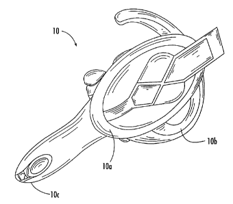
FIG. 1 is a perspective view of a wireless "Bluetooth" headset that can
incorporate
an RF filter to reduce RF coupling from a mobile wireless communications
device, in
accordance with one non-limiting example.
FIG. 2 is a block diagram showing basic functional components of a wireless or
Bluetooth headset that could be adapted to incorporate an RF filter to
decrease unwanted
audible noise, such as GSM buzz.
FIG. 3 is a schematic circuit diagram showing a combination earpiece and
filter
circuit, which could be incorporated into the earpiece shown in FIG. 2.
FIG. 4 is a schematic circuit diagram showing a combination microphone and
filter
2
CA 02563962 2006-11-O1
circuit, which could be incorporated into the microphone shown in FIG. 2.
FIG. 5 is a high-level block diagram of a Bluetooth module that could be used
in
the wireless headset shown in FIG. 2.
FIG. 6 is a high-level block diagram of an audio CODEC that could be used in
the
wireless headset shown in FIG. 2.
Detailed Description of the Preferred Embodiments
Different embodiments will now be described more fully hereinafter with
reference
to the accompanying drawings, in which preferred embodiments are shown. Many
different forms can be set forth and described embodiments should not be
construed as
limited to the embodiments set forth herein. Rather, these embodiments are
provided so
that this disclosure will be thorough and complete, and will fully convey the
scope to those
skilled in the art. Like numbers refer to like elements throughout, and prime
notation is
used to indicate similar elements in alternative embodiments.
In accordance with one non-limiting embodiment, RF filters and RF shielding
can
be implemented and applied to a microphone circuit and speaker circuit in a
wireless
"Bluetooth" headset. These types of filters and shielding can also be applied
to a power
supply circuit and other circuits to reduce the RF coupling from the wireless
communications device to those circuits used in the Bluetooth headset, which
causes the
audible unwanted noise, such as GSM buzz.
FIG. I is a perspective view of a wireless or Bluetooth headset illustrated
generally
at 10, which includes a headset body 10a that is adapted to be worn by a user
at the ear of
the user, and a pivoting, C-shaped earmount lOb that wraps around the ear.
When
wrapped around the ear, an earpiece (not shown) carried by the headset body is
engaged
against the ear and directs voice signals into the ear canal of the user. A
pivoting
microphone arm lOc supports a microphone that receives voice signals from the
user. The
illustrated wireless headset has no wires and can interact wirelessly with
different
Bluetooth compliant devices, for example, handsets, PDA's and computers. The
pivoting
microphone arm lOc and earmount lOb are foldable such that when unfolded, the
headset
is activated, allowing ready connection into received or placed calls. The
entire
headset body 10a can be worn over either ear of a user. A volume control (not
shown)
would typically remain in an upward position when it is worn.
FIG. 2 is a high-level block diagram of the wireless Bluetooth headset 11,
which
3
CA 02563962 2006-11-O1
includes a microphone 12 and earpiece 14. The microphone 12 is connected by
dual input
or audio connection lines Vin P and Vin N through a low pass filter 16 to an
audio
CODEC (COder-DECoder) 18, which converts the analog signals to and from a
digital
data stream. A feedback loop 20 extends between the audio CODEC 18 and the
microphone 12, and includes a bias line (MIC BIAS) and voltage line (MIC_VSUP)
extending to the microphone 12, forming microphone bias lines to allow
microphone bias
control signals to pass from the CODEC to the microphone. A mute switch 22 is
connected into the two lines. The audio CODEC 18 also connects to an audio
amplifier
circuit 24, which includes a volume control 26 connected in parallel. The
audio amplifier
24 passes an analog output signal to the earpiece 14 through Vout P and Vout N
signal or
audio connection lines extending between the CODEC and earpiece. A built-in
antenna
30 receives RF signals and passes them into an RF filter 32, which filters the
RF signals.
The filtered signals are received in a Bluetooth module 34, which is connected
to a
rechargeable battery 36 operative with a battery charge controller 38 and
charger input 40.
The Bluetooth module 34 is operatively connected to the audio CODEC 18. These
components as illustrated and described could be formed on a circuit board or
other
support and mounted within the headset body 10a. The different audio
connection lines
could be formed as signal or circuit traces or other means as known to those
skilled in the
art.
FIGS. 3 and 4 illustrate the type of Radio Frequency (RF) electromagnetic
interference (EMI) filters that can be used for the microphone 12 (FIG. 4) and
the earpiece
14 (FIG. 3).
FIG. 3 shows a filter for the earphone illustrating the Vout P and Vout N
signal or
audio connection lines. Each line includes an inductor element I1, I2 and
series connected
capacitor elements C1, C2. Two parallel capacitors C3 and C4 are connected as
illustrated. The inductors in each line can be formed as ferrite inductors,
including a
ferrite bead.
As shown in FIGS. 2 and 4, the microphone 12 includes an output into the low
pass filter 16 as Vin P, Vin N audio connection lines. A capacitor Cl, C2 and
an
inductor I1, I2 as an inductive coil are connected into each Vin P and Vin N
line.
Capacitors C3, C4 are connected parallel into the Vin P and Vin N lines and
positioned
on either side of capacitors C1, C2 and inductors I1, I2 as illustrated. The
feedback circuit
20 from audio CODEC 18 control includes two signal or microphone bias lines,
4
CA 02563962 2006-11-O1
MIC VSUP and MIC BIAS, and each line includes an inductive coil I3, I4 and
grounded
capacitor C5, C6, followed by another ground connected capacitor C7, C8
mounted
parallel and connected into each line as the signal enters the microphone as
illustrated.
The RF filters as described could be RF ferrite beads, serially connected
inductors,
or shunt capacitors or a combination of both. In another aspect, an isolation
RF shield as a
metallic formed enclosure or "can" could surround and isolate the microphone
or earpiece
transducer from radiating energy depending on the design. The solid line 12a,
14a in
FIGS. 3 and 4 represents the "can" that could be used.
Different types, sizes and shapes of ferrite beads can be used. Typically, a
ferrite
bead is formed from a material having a permeability controlled by the
composition of the
different oxides, for example, a ferric oxide, sometimes with nickel and zinc
added. The
ferrite beads can sometimes be formed as ferrite sleeves with two half parts
that are added
onto a signal line or a solder overcoat on a signal trace. Typically, the
longer the bead, the
better the RF suppression. The bead equivalent circuit can be a series
resistor and
inductor.
Many of the components as described can be formed as an integrated circuit and
contained within the headset body. The components can be mounted on a
dielectric
substrate, i.e., a circuit board. A circuit board could refer to any
dielectric substrate, PCB,
ceramic substrate or other circuit carrying structures for carrying signal
circuits in
electronic components. The battery 36 would typically be included within any
headset
housing for the Bluetooth headset. Ferrite beads or similar inductor
components can also
be used with modifications.
It should be understood that the RF and EMI filters as described relative to
FIGS.
2-4 can be used in many different types of Bluetooth headsets. Typically, a
Bluetooth
headset includes a Bluetooth module and is operative as a wireless technology
standard for
connecting devices to replace cables. It typically operates in radio
frequencies in the 2.5
GHz air interface and can transmit short distances of about 10 meters or less
as a class 2
device. Usually, a Bluetooth system has a bandwidth of about one megabyte per
second (1
MBPS) with individual packets of up to 2,745 bits. A class 1 Bluetooth device
could have
a signal strength up to about 100 milliwatts for a range of about 100 meters
in certain
applications.
CA 02563962 2006-11-O1
Usually three basic components are incorporated in a Bluetooth module,
including
a processor, a baseband link controller that manages core Bluetooth processes,
and a radio
that implements the 2.5 GHz air interface.
The Bluetooth architecture typically includes an application program interface
(API) libraries that are software modules that connect to host application
programs to a
Bluetooth communication system. The logical link control and adaptation
protocol
manages high level aspects of each connection, including encryption. It can
convert the
format of data between application program interfaces and lower level
Bluetooth
protocols. The link manager can manage physical details for Bluetooth
connections. The
baseband is a digital engine of a Bluetooth system. The Bluetooth radio
converts digital
baseband data to an from the 2.4 GHz analog signal typically using Gaussian
frequency
shift keying (GFSK) modulation.
FIG. 5 is a block diagram of a typical Bluetooth module 100 that can be used
with
the different embodiments of a Bluetooth headset. As illustrated, a
receive/transmit
(Rx/Tx) switch 102 receives signals from an antenna 104 (which could
correspond to
antenna 30 described relative to FIG. 2) and is operative with a Bluetooth
transceiver 106,
operative with Bluetooth components that receive clock signals and are
operative with a
CODEC interface and Host interface. These functional components include a
Bluetooth
baseband circuit 110, peripherals circuit 112, ROM 114 and RAM 116, a RISC
processor
118 and clock and power management circuit 120. Of course, many other
components
could be used as known to and suggested by those skilled in the art. An
example of such a
functional Bluetooth module is a BRF 6100/6150 Bluetooth module manufactured
by
Texas Instruments.
Different types of CODEC's can also be used in the circuit shown in FIG. 2,
and
an example CODEC is shown in FIG. 6 at 200, and could be used in a Bluetooth
headset
and operative with the Bluetooth module. For example, as illustrated, the
CODEC could
include an analog input into a S/H (Sample/Hold) amplifier 202 that passes to
a successive
approximations companding analog-to-digital converter (ADC) 204. A shift
register 206
receives the signal from the successive approximations companding ADC 204 and
produces a serial digital data output. A clock signal is applied to the shift
register 206 and
also applied to a second shift register 210 that sends data to a companding
digital-to-
analog converter (DAC) 212 that transmits the converted signal through a
buffer amplifier
6
CA 02563962 2006-11-O1
214 as an analog output. Serial digital data input is received in the second
shift register.
N-bit parallel data pass between components as illustrated.
The CODEC could include a transmit functional component that includes an
analog input, amplifier, filters, sample and hold circuit comparator,
successive
approximation circuit, and an output register with feedback and control logic.
The
CODEC could also include a receive function that includes an input register,
digital-to-
analog converter (DAC), receive control logic that inputs into a sample and
hold (S/H)
circuit, which is buffered and filtered using an adder and gain set logic.
General control
logic could be operative with the digital-to-analog converter and receive
control logic.
The sample and hold circuit could receive a reference.
It should also be understood that the CODEC can use delta modulation to
minimize
the effects of noise without increasing the number of bits being transmitted.
Adaptive
delta modulation could also be used, which aids in overcoming the slope
overload problem
by varying the step size such that the quantized signal more closely follows
the original
signal.
Many modifications and other embodiments of the invention will come to the
mind
of one skilled in the art having the benefit of the teachings presented in the
foregoing
descriptions and the associated drawings. Therefore, it is understood that the
invention is
not to be limited to the specific embodiments disclosed, and that
modifications and
embodiments are intended to be included within the scope of the appended
claims.
7