Note: Descriptions are shown in the official language in which they were submitted.
CA 02564410 2006-10-17
CIRCUIT AND METHOD FOR REDUCING STORED ENERGY IN AN
ELECTROSURGICAL GENERATOR
BACKGROUND
1. Field
The present disclosure relates generally to electrosurgical system, and more
specifically, to a system and method for discharging excess energy of a high
voltage direct
current (HVDC) power supply of an electrosurgical generator
2. Description of the Related Art
Electrosurgery involves application of high radio frequency electrical current
to a
surgical site to cut, seal, ablate, or coagulate tissue. In monopolar
electrosurgery, a source or
active electrode delivers radio frequency energy from the electrosurgical
generator to the
tissue and a return electrode carries the current back to the generator. In
monopolar
electrosurgery, the source electrode is typically part of a surgical
instrument held by the
surgeon and applied to the tissue to be treated. A patient return electrode is
placed remotely
from the active electrode to carry the current back to the generator.
In bipolar electrosurgery, a hand-held instrument typically carries two
electrodes, e.g.,
electrosurgical forceps. One of the electrodes of the hand-held instrument
functions as the
active electrode and the other as the return electrode. The return electrode
is placed in close
proximity to the active (i.e., current supplying) electrode such that an
electrical circuit is
formed between the two electrodes. In this manner, the applied electrical
current is limited to
the body tissue positioned between the two electrodes.
CA 02564410 2006-10-17
Conventional electrosurgical generators include a high voltage direct current
(HVDC)
power connected to a radio frequency (RF) output stage, which converts DC
energy generated
by the HVDC into RF energy. The high voltage direct current (HVDC) power
supply
includes an output filter which smoothes the switching of the HVDC into a DC
level. This
filter can store large amount of energy and under light loads and high
impedance, the
discharge of the output filter is slow. As a result, the generator response
time is significantly
lowered thereby limiting the generator's ability to pulse energy rapidly or
respond quickly
during light loads.
Therefore, there is a need for an electrosurgical generator which can
discharge energy
to in a consistent and rapid manner under various load conditions, including
light loads and high
impedance.
SUMMARY
The present disclosure provides for an electrosurgical generator which
includes a
circuit for discharging stored energy and a high voltage power supply. The
active discharge
15 circuit includes a pulse width modulator, a load having a resistive element
and a switching
circuit, and an error signal generating circuit. The error generating circuit
determines a
difference between and output set point voltage and feedback voltage and
generates an error
signal. If the error signal is less than a first predetermined threshold the
switching circuit
switches in a load and sinks current supplied by the high voltage power supply
through the
20 load. If the signal is above a second predetermined threshold the pulse
width modulator is
switched on. This ensures that the pulse width modulator and the load are not
active
simultaneously.
2
CA 02564410 2006-10-17
According to one embodiment of the present disclosure a circuit for
'discharging
stored energy in an electrosurgical generator is disclosed. The circuit
includes a pulse width
modulator for controlling a high voltage power supply, an error signal
generating circuit
configured for delivering an error signal as a difference between an output
signal voltage with
a feedback voltage generated by the high voltage power supply. The error
signal is
transmitted to the pulse width modulator when the error signal is large enough
the pulse
width modulator turns on. The circuit further includes a switching circuit
configured to
switch in a load in parallel with an output of the high voltage power supply
when the error
signal is lesser than a first predetermined threshold to discharge the output.
to According to another embodiment of the present disclosure an
electrosurgical
generator is disclosed. The generator includes a high voltage power source for
generating
direct current, a radio frequency output stage for converting direct current
into radio
frequency energy, and a circuit for discharging stored energy. The circuit
includes a pulse
width modulator for controlling a high voltage power supply, an error signal
generating
15 circuit configured for delivering an error signal as a difference between
an output signal
voltage with a feedback voltage generated by the high voltage power supply.
The error signal
is transmitted to the pulse width modulator. The circuit further includes a
switching circuit
configured to switch in a load in parallel with an output of the high voltage
power supply
when the error signal is lesser than a first predetermined threshold to
discharge the output.
2o According to a further aspect of the present disclosure a method for
discharging
energy stored in a circuit in an electrosurgical generator is disclosed. The
method comprises
the steps of deriving an error signal as a difference between an output
setpoint voltage with a
feedback voltage generated by a high voltage power supply, comparing the error
signal with a
CA 02564410 2006-10-17
first predetermined threshold, switching on a load in parallel with an output
of the high
voltage power supply when the error signal is lesser than a first
predetermined threshold to
discharge the output, and switching on a pulse width modulator if the error
signal is above a
second predetermined threshold.
BRIEF DESCR1PTION OF THE DRAWINGS
The above and other aspects, features, and advantages of the present
disclosure will
become more apparent in light of the following detailed description when taken
in
conjunction with the accompanying drawings in which:
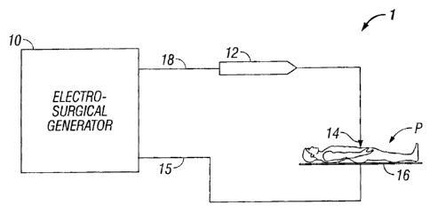
Fig. 1 is a schematic block diagram of one embodiment of an electrosurgical
system
1o according to the present disclosure;
Fig. 2 is a schematic block diagram of a generator according to the present
disclosure;
Fig. 3 is a schematic block diagram of a high voltage direct current (HVDC)
power
supply according to the present disclosure;
Fig. 4 is a circuit diagram of the HVDC power supply according to the present
15 disclosure; and
Figs. SA-F are graphs of the HVDC response with sinusoidal input and output
waveforms generated by the HVDC power supply of the present disclosure.
DETAILED DESCRIPTION
Preferred embodiments of the present disclosure will be described herein below
with
2o reference to the accompanying drawings. In the following description, well-
known functions
or constructions are not described in detail to avoid obscuring the present
disclosure in
unnecessary detail.
4
CA 02564410 2006-10-17
The present disclosure provide for an elcctrosurgical generator including a
high
voltage power supply for supplying a DC voltage, an output filter, and an
active discharge
circuit for effectively discharging stored energy in the output filter. The
active discharge
circuit switches in a load in parallel with the output filter so that energy
stored in the output
filter is discharged in consistent manner regardless of the resistance of the
external load.
The generator according to the present disclosure can be used with bipolar and
monopolar electrosurgical devices. Fig. 1 is a schematic illustration of a
monopolar
electrosurgical system 1. The system 1 includes an active electrode 14 and a
return electrode
16 for treating tissue of a patient P. Electrosurgical RF energy is supplied
to the active
to electrode 14 by a generator 10 via a cable 18 allowing the active electrode
14 to ablate, cut or
coagulate the tissue. The return electrode 16 is placed at the patient P to
return the energy
from the patient P to the generator 10 via a cable 15.
The generator 10 may include input controls (e.g., buttons, activators,
switches, etc.)
for controlling the generator 10. The controls allow the surgeon to adjust
power of the RF
15 energy, waveform, and other parameters to achieve the desired wavefornl
suitable for a
particular task (e.g., cutting, coagulating, etc.). Disposed between the
generator 10 and the
active electrode 14 on the cable 18 is a hand piece 12, which includes a
plurality of input
controls which may be redundant with certain input controls of the generator
10. Placing the
input controls at the hand piece 12 allows for easier and faster modification
of RF energy
2o parameters during the surgical procedure without having the surgeon divert
his attention from
the surgical site and returning to the generator 10.
Fig. 2 shows a schematic block diagram of the generator 10 having a controller
26, a
high voltage DC power supply (HVDC) 28, and an RF output stage 30. The
controller 26
CA 02564410 2006-10-17
includes a microprocessor and an output port of the microprocessor is
electrically connected
to the HVDC 28. The HVDC 28 is configured to supply DC power to the RF output
stage 30.
The controller 26 receives input signals from the generator 10 and/or hand
piece 12, e.g., a set
point, and the controller 26 in turn adjust power outputted by the generator
10, more
specifically the HVDC 28, and/or performs other control functions thereon.
The RF output stage 30 converts DC power into RF energy and delivers the RF
energy
to the active electrode 14. In addition, the RF output stage 30 also receives
RF energy from
the return electrode 16. The power of the HVDC 28 can be varied to modify RF
magnitude
(e.g., amplitude) thereby adjusting the power of the RF energy delivered to
the tissue. This
1o allows for accurate regulation of the power of delivered RF energy.
Regulation of output energy is controlled by the controller 26 (e.g., a
microprocessor)
using algorithms and/or software. The controller 26 forms a closed-control
loop with a
sensor 29 which senses various tissue and output energy properties and reports
the properties
data to the controller 26. The closed-control loop allows for real-time
adjustment of output
15 energy based on the properties sensed by the sensor 29. More specifically,
the closed-control
loop can process signals from the sensor 29 and make corresponding adjustments
in about
250 ps. The HVDC 28 is capable of supplying and discharging the current at
similar rates
(e.g., sourcing at about 300 V/ms or faster and discharging at about 7 V/ms or
faster).
With reference to Fig. 3, discharging of current is accomplished using an
active
20 discharge circuit (ADC) 31 - a component of the HVDC 28 - which is a
circuit that
switches a load 36 (e.g., one or more resistors) in parallel with an output
capacitor 34. The
HVDC 28 includes a diode 33 on an output connection 35 which allows current to
flow away
from the HVDC 28 into a filter 32. The load 36 discharges the energy stored in
the capacitor
6
CA 02564410 2006-10-17
34. During discharge, the diode 33 prevents the discharged current to flow
back into the
HVDC 28 thereby directing the current toward the active electrode 14.
Fig. 4 shows the ADC 31 in more detail and other components of the generator
10.
The output and input connections 35, 37 include a plurality of diodes 33 which
block the
output current from returning to the HVDC 28 during discharge. The HVDC 28 is
connected
to a pulse width modulator 38, which may be a Pulse Width Modulator UCC3895
available
from Texas Instruments, for controlling the output of the HVDC 28. The pulse
width
modulator 38 implements control of a full-bridge power stage 33 by phase
shifting the
switching of one half bridge with respect to the other. It allows constant
frequency pulse-
1o width modulation in conjunction with resonant zero-voltage switching to
provide high
efficiency at high frequencies and can be used either as a voltage mode or
current mode
controller.
The pulse width modulator 38 is configured to receive an error signal which is
generated by an error signal generating circuit, a first comparator 52. The
error signal is
15 derived from the difference between the output set point of the HVDC 28
(e.g., ECON) - the
intended output voltage - and the voltage feedback of the HVDC 28 (VFB) -
actual output
voltage generated by the HVDC 28. If VFB is higher than ECON, without the ADC
31, the
signal would be OV. This causes the loop to be delayed as it waits for the
signal to increase in
order to activate the pulse width modulator 38. The ADC 31 avoids that problem
and
2o maintains the signal from dropping too low because the ADC 31 discharges
the output of the
HVDC 28 faster than the signal may drop. The error signal is sent to the shift
controller 38
which compares the error signal with a second predetermined signal. If the
signal drops below
the second predetermined threshold, about 0.7V, the pulse width modulator 38
shuts down
7
CA 02564410 2006-10-17
and the ADC 31 becomes operational. When the pulse width modulator 38 shuts
down, the
HVDC 28 stops sourcing current.
The signal is also compared against a first predetermined threshold, about
O.SV, at a
second comparator 50. Thus, if the signal is below this level the ADC 31 will
turn on. This
ensures that the pulse width modulator 38 will not be turned on when the ADC
31 is on
thereby reducing chance of HVDC 28 driving into the ADC 31. The signal feeding
into the
second comparator 50 is not filtered, this allows for a relatively fast
response from the ADC
31. The time period between pulse width modulator 38 shutting down and the ADC
31
starting up, or vice versa, is about 5 ps.
to As discussed above, the capacitor 34 is in parallel with the load 36 which
is used to
discharge the current. The load 36 provides a gate drive voltage and includes
a switching
component 40 and a resistive element 42. The switching component 40 can be a
transistor,
such as a field-effect transistor (FET), metal-oxide semiconductor field-
effect transistor
(MOSFET), insulated gate bipolar transistor (IGBT), relay, and the like. The
resistive
15 element 42 is in series with the switching component 40 and to ground 44,
which is known as
a source follower. The source follower limits amount of current which flows
through the
resistive element 42. As amount of current flowing through the resistive
element 42
increases, the voltage across the resistive element 42 increases as well. This
voltage subtracts
from the gate drive voltage as the current reaches a predetermined threshold
causing the
2o switching component 40 to turn off thereby acting as a variable resistor.
The resistive
element 42 has a resistance, such as about S Ohms, which will limit the
current to less than
about 2 Amps. For instance, the resistive element 42 has a turn on around 2.V
and 2A and will
8
CA 02564410 2006-10-17
subtract lOB (2A * 5 Ohms) from the 12V gate drive. This reduces the stress on
HVDC 28
and other output components.
Examples
Figs. 5A-E are graphs of HVDC 28 output. Fig. 5A shows output response of the
HVDC 28 without the ADC 31 while Fig. 5B shows output response of the HVDC 28
equipped with the ADC 31. Waveform 60 represents ECON voltage (e.g., the
intended
output voltage) that fluctuates from about 0.5V and about 1V. Wavefonn 62 is
the actual
signal voltage output (e.g., voltage feedback) which is a 1 KHz sine wavefonn
of the HVDC
28 into a load of about 200 Ohms. In Fig. 5A, waveforms 60, 62 do not track
each other,
representing delay in discharging of the current. In Fig. 5B, waveforms 60, 62
closer track
each other due to faster discharging caused by the ADC 28.
Figs. SC-D shows a waveform 64 which represents gate drive of the switching
component 40. When the gate drive waveform 64 shows a rise it is
representative of the
switching component 40 being on thereby activating a 5 Ohm load across the
output. In Fig.
5C, the gate drive pulses on and off very rapidly, such as during the downward
sloping
portion of the wavefonns 60, 62 the gate drive is on and off during the upward
sloping
portion of the wavefornls 60, 62. Fig. 5D shows an expanded view of the gate
drive shows the
rate of the pulsing, which is about 230 KHz. This demonstrates that the ADC 28
is
maintaining the signal from falling below 0.5V.
Figs. 5E-F show time differences between the waveforms 60, 62, 64. More
specifically, Fig. 5E shows the time period between the pulse width modulator
28 turning off
and the ADC 31 turning on is about 4 ~s, while Fig. 5F shows the time period
between the
pulse width modulator 28 turning on and the ADC 31 turning offis also about 15
ps. This
9
CA 02564410 2006-10-17
demonstrates that the ADC 31 and the pulse width modulator 28 are not
activated at the same
time, which reduces the risk of over-stressing components of the generator 10.
The described embodiments of the present disclosure are intended to be
illustrative
rather than restrictive, and are not intended to represent every embodiment of
the present
disclosure. Various modifications and variations can be made without departing
from the
spirit or scope of the disclosure as set forth in the following claims both
literally and in
equivalents recognized in law.