Note: Descriptions are shown in the official language in which they were submitted.
CA 02564428 2009-04-14
TITLE OF THE INVENTION
COATED ARTICLE WI I'H OXIDATION GRADED LAYER PROXIMATE
IR REFLECTING LAYER(S) AND CORRESPONDING METHOD
[0001) This invention relates to a coated article including a low-E coating,
which includes, for example, a graded layer (e.g., oxidation graded layer). In
certain
example embodiments, the graded layer is graded in a manner such that it
becomes
less oxidized closer to an infrared (IR) reflecting layer. In certain example
embodiments, a sputtered layer comprising at least one metal may be ion beam
treated
in order to introduce oxygen into the layer thereby forming the oxidation
graded layer.
Coated articles according to certain example embodiments of this invention may
be
used in the context of vehicle windshields, insulating glass (IG) window
units, other
types of windows, or in any other suitable application.
BACKGROUND OF THE INVENTION
[0002] Coated articles are known in the art for use in window application such
as insulating glass (IG) window units, vehicle windows, and/or the like. It is
known
that in certain instances, it is sometimes desirable to heat treat (e.g.,
thermally temper,
heat bend and/or heat strengthen) such coated articles for purposes of
tempering,
bending, or the like in certain example instances. Example non-limiting low-
emissivity (low-E) coatings are illustrated and/or described in U.S. Patent
Document
Nos. 6,723,211; 6,576,349; 6,447,891; 6,461,731; 3,682,528; 5,514,476;
5,425,861;
and 2003/0150711.
[00031 In certain situations, designers of coated articles with low-E coatings
often strive for a combination of high visible transmission, substantially
neutral color,
low emissivity (or emittance), and low sheet resistance (R,), High visible
transmission for example may permit coated articles to be more desirable in
applications such as vehicle windshields or the like, whereas tow-emissivity
(low-E)
and low sheet resistance characteristics permit such coated articles to block
significant
1
CA 02564428 2009-04-14
amounts of IR radiation so as to reduce for example undesirable heating of
vehicle or
building interiors.
(0004] The use of oxidation graded layer(s) in low-E coatings is known. For
example, see commonly owned U.S. Patent Nos. 6,376,349 and 6,723,211. The '349
Patent, for example, explains that a contact layer(s) is oxidation graded so
as to
become less oxidized closer to an IR reflecting layer of a material such as
silver. The
'349 Patent explains, for example, that oxidation grading of contact layer(s)
is
advantageous in that it permits high visible transmission to be achieved in
combination with optional heat treatability.
100051 However, the oxidation grading of a NiCrOX contact layer(s) is
typically formed by sputtering. For example, more oxygen gas may be introduced
via
one side of a NiCr sputtering target compared to another side of the target,
thereby
resulting in oxidation grading of the NMCrOX layer being sputter-deposited.
While this
typically works very well, there are certain drawbacks. First, while
sputtering a NiCr
target in an oxygen inclusive atmosphere tends to cause significant amounts of
chromium oxide to form in the resulting layer, the nickel does not so easily
become
nickel oxide (i.e., much Ni may remain in metallic form in the resulting
layer). This
can sometimes be undesirable in that metallic Ni tends to reduce visible
transmission
of the resulted coated article. Second, the use of large amounts of oxygen in
a
sputtering zone of a sputter coater sometimes causes undesirable target
flaking to
occur.
100061 In view of the above, it will be apparent to those skilled in the art
that
there exists a need for a technique for forming an oxidation graded layer in a
coating
in a more efficient manner. In certain example instances, there exists a need
for a
technique for forming an oxidation graded layer in a coating in a manner which
results in: (a) more oxidation of Ni if a NiCr target or the like is used in
sputtering; (b)
less oxygen being required in a given zone(s) or bay(s) of a sputter coater,
and/or (c)
reduction or elimination of the flaking effect problem.
2
CA 02564428 2006-10-26
WO 2005/115941 PCT/US2005/014106
BRIEF SUMMARY OF EXAMPLE EMBODIMENTS OF THE INVENTION
[0007] In certain example embodiments of this invention, ion beam treatment
is used to control and/or modify stoichiometry of a layer(s) in a coating
(i.e.,
stoichiometry modification and/or control). The layer(s) to be modified may be
deposited on a substrate such as a glass substrate, and other layer(s) may or
may not
be located between the glass substrate and the layer(s) to be modified by ion
treatment. In certain example embodiments, the ion treatment may utilize at
least
oxygen ions. When oxygen ions are used to ion beam treat an originally
deposited
metal layer or slightly oxided layer, an oxidation graded layer may result.
[0008] In certain example embodiments of this invention, an oxidation graded
layer in a solar control coating may be formed in the following manner. First,
a layer
is sputter-deposited on a substrate (either directly on the substrate, or
alternatively on
the substrate over other layer(s)). Then, the sputter-deposited layer is
subjected to an
ion beam treatment, wherein the ion beam includes at least oxygen ions. The
oxygen
inclusive ion beam treatment introduces oxygen ions into the sputter-deposited
layer.
The ion beam is directed at the layer in a manner so as to create an oxidation
graded
effect in the layer such that the layer following the ion beam treatment is
more
metallic closer to an infrared (IR) reflecting layer than at a location
further from the
IR reflecting layer. The oxidation graded layer has improved (higher) visible
transmission, and due to its more metallic nature closer to the IR reflecting
layer is
able to better protect the IR reflecting layer during potential heat treatment
such as
thermal tempering or heat strengthening.
[0009] In certain example embodiments of this invention, there is provided a
method of making a coated article, the method comprising: providing a glass
substrate; sputtering a layer comprising silver on the glass substrate;
sputtering a layer
comprising NiCr on the substrate over the layer comprising silver, so that the
layer
comprising NiCr contacts the layer comprising silver; ion beam treating at
least an
upper surface of the layer comprising NiCr with at least oxygen ions so that
following
said ion beam treating the layer comprising NiCr is more oxidized at a
location further
from the layer comprising silver than at a location closer to the layer
comprising
3
CA 02564428 2006-10-26
WO 2005/115941 PCT/US2005/014106
silver; and following said ion beam treating, sputtering at least a dielectric
layer over
the layer comprising NiCr.
[0010] In other example embodiments of this invention, there is provided a
method of making a coated article, the method comprising: providing a glass
substrate; sputtering an IR reflecting layer on the glass substrate;
sputtering a layer
comprising Ni and/or Cr on the glass substrate over the IR reflecting layer;
and ion
beam treating at least an upper surface of the layer comprising Ni and/or Cr
with at
least oxygen so that following said ion beam treating the layer comprising Ni
and/or
Cr is more oxidized at a location further from the IR reflecting layer than at
a location
closer to the IR reflecting layer.
[0011] In still other example embodiments of this invention, there is provided
a method of making a coated article, the method comprising: providing a
substrate;
forming a layer comprising at least one metal on the substrate; ion beam
treating at
least an upper surface of the layer comprising the at least one metal so that
following
said ion beam treating the layer is more oxidized at a location further from
the
substrate than at a location closer to the substrate.
[0012] In other example embodiments of this invention, there is provided a
method of making a coated article, the method comprising: providing a glass
substrate; sputtering a layer on the glass substrate; ion beam treating at
least an upper
surface of the layer on the glass substrate with at least one reactive gas so
as to
modify a stoichiometry thereof; and following said ion beam treating
sputtering at
least another layer over the layer that has been ion beam treated.
BRIEF DESCRIPTION OF THE DRAWINGS
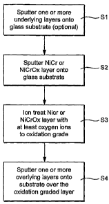
[0013] FIGURE 1 is a flowchart illustrating certain steps carried out in
making a coated article according to an example embodiment of this invention.
[0014] FIGURE 2 is a cross sectional view of a coated article according to an
example embodiment of this invention.
4
CA 02564428 2006-10-26
WO 2005/115941 PCT/US2005/014106
[0015] FIGURE 3 is a cross sectional view of a coated article according to an
example embodiment of this invention, in a mid-production step, being ion beam
treated with at least oxygen ions in order to form an oxidation graded layer.
[0016] FIGURE 4 is a cross sectional view of a portion of a coated article
according to an example embodiment of this invention, following ion beam
treatment,
illustrating an oxidation graded layer formed via at least the ion beam
treatment.
[0017] FIGURE 5(a) is a graph illustrating the oxidation grading of a NiCrOX
layer according to an example of the instant invention, following ion beam
treatment
with oxygen ions.
[0018] FIGURE 5(b) is a graph illustrating the relative amounts of oxided Cr
as a function of depth comparing (a) an ion beam treated layer originally
sputter-
deposited as NiCr and then ion beam treated with oxygen ions, versus (b) a
pair of
sputter-deposited NiCrOX layers each sputter deposited in an oxygen inclusive
atmosphere without ion beam treatment.
[0019] FIGURE 6 is a cross sectional view of an example ion source that may
be used to ion beam treat layers according to example embodiments of this
invention.
[0020] FIGURE 7 is a perspective view of the ion source of Fig. 6.
[0021] FIGURES 8(a) and 8(b) are cross sectional views of different oxidation
graded layers according to different example embodiments of this invention.
[0022] FIGURE 9 is a graph illustrating the amount of Ni oxided by ion beam
treatment compared to merely sputtering in an oxygen inclusive atmosphere.
DETAILED DESCRIPTION OF EXAMPLES OF THE INVENTION
[0023] Coated articles herein may be used in applications such as vehicle
windshields, monolithic windows, IG window units, and/or any other suitable
application that includes single or multiple glass substrates. In vehicle
windshield
applications, for example, a pair of glass substrates may be laminated
together with a
polymer based layer of a material such as PVB, and the coating is provided on
the
interior surface of one of the glass substrates adjacent the polymer based
layer. In
certain example embodiments of this invention, the coating includes a double-
silver
CA 02564428 2006-10-26
WO 2005/115941 PCT/US2005/014106
stack, although this invention is not so limited in all instances (e.g.,
single silver
stacks may also be used in accordance with certain embodiments of this
invention).
[0024] In certain example embodiments of this invention, ion beam treatment
is used to control and/or modify stoichiometry of a layer(s) in a coating
(i.e.,
stoichiometry modification and/or control). The layer(s) to be modified may be
deposited on a substrate such as a glass substrate, and other layer(s) may or
may not
be located between the glass substrate and the layer(s) to be modified by ion
beam
treatment. In certain example embodiments, the ion beam treatment may utilize
at
least oxygen ions. When oxygen ions are used to ion beam treat an originally
deposited metal layer or slightly oxided layer, an oxidation graded layer may
result.
[0025] In certain example embodiments of this invention, an oxidation graded
layer in a solar control coating may be formed in the following manner. First,
a layer
is sputter-deposited on a substrate (either directly on the substrate, or
alternatively on
the substrate over other layer(s)). This layer in certain example embodiments
may be
originally sputter-deposited as including or of NiCr of NiCrOX, although this
invention is not so limited. Then, the sputter-deposited layer is subjected to
an ion
beam treatment, wherein the ion beam includes at least oxygen ions in certain
example embodiments. The ion beam may be a focused ion beam, a collimated ion
beam, or a diffused ion beam in different embodiments of this invention. The
oxygen
inclusive ion beam treatment introduces oxygen ions into the sputter-deposited
layer,
thereby creating an oxidation graded effect in the layer such that the layer
following
the ion beam treatment is more metallic closer to an infrared (IR) reflecting
layer than
at a location further from the IR reflecting layer. The portion of the layer
closest to
the IR reflecting layer may be entirely metallic in certain example instances
or
alternatively may be relatively less oxided compared to other parts of the
layer in
other example embodiments of this invention.
[0026] The oxidation graded layer has improved (higher) visible transmission
(compared to a purely metallic layer), and due to its more metallic nature
closer to the
IR reflecting layer is able to better protect the IR reflecting layer during
optional heat
treatment such as thermal tempering, heat bending, and/or heat strengthening.
Moreover, it has surprisingly been found that ion beam plasma (including at
least
6
CA 02564428 2006-10-26
WO 2005/115941 PCT/US2005/014106
oxygen) is able to oxidize a higher amount of Ni atoms compared to merely
sputtering
in an oxygen inclusive atmosphere. In particular, merely sputtering NiCr
target(s) in
an oxygen inclusive atmosphere tends to oxide Cr atoms more than Ni atoms. The
use of the ion beam treatment herein tends to permit more Ni to be oxided in
the end
layer. Again, this helps to improve transmission characteristics of the
coating,
without sacrificing heat treatability in certain example embodiments of this
invention.
Moreover, another unexpected advantage of certain embodiments of this
invention is
that it has unexpectedly been found that a more metallic part of the oxidation
graded
layer sticks better to the IR reflecting layer (e.g., Ag layer), whereas a
more oxidized
part sticks better to the overlying dielectric layer(s). Thus, ion beam plasma
irradiation herein improves adhesion and thus durability of the coated article
as an
additional advantage. Yet another advantage associated with certain
embodiments of
this invention is that growing NiCrOX from metallic NiCr target(s) in oxygen
inclusive
atmosphere can result in more particulates than originally sputtering NiCr in
a
substantially inert atmosphere to provide a substantially metallic layer,of
NiCr and
then ion beam treating the substantially metallic layer in order to oxide the
same.
[0027] This type of oxidation grading of a layer may be performed on one or
more layers of a given coating in different embodiments of this invention.
[0028] Coated articles according to different embodiments of this invention
may or may not be heat treated (HT) in different instances. The terms "heat
treatment" and "heat treating" as used herein mean heating the article to a
temperature
sufficient to achieve thermal tempering, heat bending, and/or heat
strengthening of the
glass inclusive article. This definition includes, for example, heating a
coated article
in an oven or furnace at a temperature of least about 580 degrees C, more
preferably
at least about 600 degrees C, for a sufficient period to allow tempering,
bending,
and/or heat strengthening. In certain instances, the HT may be for at least
about 4 or
minutes.
[0029] Fig. 1 is a flowchart illustrating certain steps carried out according
to
an example embodiment of this invention. Initially, a glass substrate is
provided.
One or more underlying layers is/are then deposited (e.g., sputter deposited)
onto the
glass substrate (Si). For example, in embodiments where a plurality of
underlayers
7
CA 02564428 2006-10-26
WO 2005/115941 PCT/US2005/014106
are provided, a first dielectric layer may be deposited on the substrate and
thereafter
an IR reflecting layer of a material such as Ag, Au or the like may be
deposited on the
substrate over at least the first dielectric layer. Then, a layer such as a
contact layer of
or including NiCr is sputter-deposited on the glass substrate over the
underlying
layer(s) (S2). While this sputter-deposited layer is ultimately to be
transformed into a
type of oxidation graded layer, it is typically originally sputter-deposited
in a manner
where it is not significantly oxidation graded (although it may be oxidation
graded to
some extent as originally sputter-deposited in other example embodiments).
This
layer may be originally sputter deposited as a layer of or including NiCr, Ni,
NiCrOX
or any other suitable material.
[0030] Still referring to Fig. 1, after step S2 has been completed, the layer
sputter-deposited in step S2 is then treated with an ion beam including at
least oxygen
ions (S3). This ion beam treatment introduces at least oxygen ions into the
layer
deposited in step S2. An ion energy of the ion source is utilized which will
cause the
vast majority of oxygen ions to make their way only part-way through the layer
originally sputter-deposited in step S2. Since the vast majority of oxygen
ions make
their way through only part of the layer, the layer becomes oxidation graded
since the
part of the layer farthest from the ion source is much less oxided (if at all)
than those
portions closer to the ion source. After the layer has been ion beam treated
and thus
oxidation graded, addition overlying layer(s) are then sputter-deposited over
the
oxidation graded layer (S4). For example, one or more dielectric layers may be
sputter-deposited over the graded layer in step S4 in certain example
embodiments of
this invention.
[0031] Figure 2 is a side cross sectional view of a coated article according
to
an example non-limiting embodiment of this invention. The coated article
includes
substrate 1 (e.g., clear, green, bronze, or blue-green glass substrate from
about 1.0 to
10.0 mm thick, more preferably from about 1.0 mm to 3.5 mm thick), and a low-E
coating (or layer system) 2 provided on the substrate 1 either directly or
indirectly.
The coating (or layer system) 2 includes, in this example embodiment:
dielectric
silicon nitride layer 3 which may be of Si3N4, of the Si-rich type for haze
reduction, or
of any other suitable stoichiometry of silicon nitride in different
embodiments of this
8
CA 02564428 2009-04-14
invention, first lower contact layer 7 (which contacts IR reflecting layer 9),
first
conductive and preferably metallic or substantially metallic infrared (IR)
reflecting
layer 9, first upper contact layer 11' (which contacts layer 9), dielectric
layer 13
(which may be deposited in one or multiple steps in different embodiments of
this
invention), another silicon nitride layer 14, second lower contact layer 17
(which
contacts IR reflecting layer 19), second conductive and preferably metallic IR
reflecting layer 19, second upper contact layer 21' (which contacts layer 19),
dielectric
layer 23, and finally protective dielectric layer 25. The "contact" layers 7,
11, 17 and
21 each contact at least one IR reflecting layer (e.g., layer based on Ag).
The
aforesaid layers 3-25 make up tow-E (i.e., low emissivity) coating 2 which is
provided
on glass or plastic substrate 1.
100321 In monolithic instances, the coated article includes only one glass
substrate 1 as illustrated in Fig. 2. However, monolithic coated articles
herein may be
used in devices such as laminated vehicle windshields, IG window units, and
the like.
A laminated vehicle window such as a windshield includes first and second
glass
substrates laminated to one another via a polymer based interlayer (e.g., see
US
6,686,050). One of these substrates of the laminate may support coating 2 on
an
interior surface thereof in certain example embodiments. As for IG window
units, an
IG window unit may include two spaced apart substrates 1. An example IG window
unit is illustrated and described, for example, in U.S. Patent No. 6,632,491.
An
example IG window unit may include, for example, the coated glass substrate 1
shown in fig. 2 coupled to another glass substrate via spacer(s), sealant(s)
or the like
with a gap being defined therebetween. This gap between the substrates in 1G
unit
embodiments may in certain instances be filled with a gas such as argon (Ar).
An
example IG unit may comprise a pair of spaced apart clear glass substrates
each about
4 mm thick one of which is coated with a coating herein in certain example
instances,
where the gap between the substrates may be from about 5 to 30 mm, more
preferably
from about 10 to 20 mm, and most preferably about 16 mm. In certain example
instances, the coating 2 may be provided on the interior surface of either
substrate
facing the gap.
9
CA 02564428 2009-04-14
[00331 In certain example embodiments of this invention, one or both of upper
contact layer(s) i i' and/or 21' is oxidation graded. Thus, at least one of
NiCr
inclusive contact layers 11' and/or 21' has been ion beam treated with at
least oxygen
ions in order to oxidation graded the same in certain example embodiments of
this
invention.
10034] Example details relating to layers 3, 7, 9, 13, 14, 17, 19, 23 and 25
of
the Fig. 2 coating are discussed in U.S. Patent No. 7,344,782. For example,
dielectric
layers 3 and 14 may be of or include silicon nitride in certain embodiments of
this
invention. Silicon nitride layers 3 and 14 may, among other things, improve
heat-
treatability of the coated articles, e.g., such as thermal tempering or the
like. The
silicon nitride of layers 3 and/or 14 may be of the stoichiometric type
(Si3N4) type, or
alternatively of the Si-rich type in different embodiments of this invention.
Any
and/or all of the silicon nitride layers discussed herein may be doped with
other
materials such as stainless steel or aluminum in certain example embodiments
of this
invention. For example, any and/or all silicon nitride layers discussed herein
may
optionally include from about 0-15% aluminum, more preferably from about I to
10%
aluminum, most preferably from 1-4% aluminum, in certain example embodiments
of
this invention. The silicon nitride may be deposited by sputtering a target of
Si or
SiAI in certain embodiments of this invention.
100351 Infrared (IR) reflecting layers 9 and 19 are preferably substantially
or
entirely metallic and/or conductive, and may comprise or consist essentially
of silver
(Ag), gold, or any other suitable IR reflecting material. IR reflecting layers
9 and 19
help allow the coating to have low-E and/or good solar control
characteristics. The IR
reflecting layers may, however, be slightly oxidized in certain embodiments of
this
invention. Dielectric layer 13 may be of or include tin oxide in certain
example
embodiments of this invention. However, as with other layers herein, other
materials
may be used in different instances. Lower contact layers 7 and/or 17 in
certain
embodiments of this invention are of or include zinc oxide (e.g., ZnO). The
zinc
oxide of layer(s) 7, 17 may contain other materials as well such as Al (e.g.,
to form
ZnALO,). For example, in certain example embodiments of this invention, one or
CA 02564428 2006-10-26
WO 2005/115941 PCT/US2005/014106
more of zinc oxide layers 7, 17 may be doped with from about 1 to 10% Al, more
preferably from about 1 to 5% Al, and most preferably about 2 to 4% Al. The
use of
zinc oxide 7, 17 under the silver 9, 19 allows for an excellent quality of
silver to be
achieved.
[0036] Dielectric layer 23 may be of or include tin oxide in certain example
embodiments of this invention. However, layer 23 is optional and need not be
provided in certain example embodiments of this invention. Dielectric layer
25,
which may be an overcoat including one or more layers in certain example
instances,
may be of or include silicon nitride (e.g., Si3N4) or any other suitable
material in
certain example embodiments of this invention. Optionally, other layers may be
provided above layer 25. Optionally, a silicon nitride inclusive layer 25
maybe
located directly on an over oxidation graded layer 21'. Layer 25 is provided
for
durability purposes, and to protect the underlying layers during heat
treatment and/or
environmental use. In certain example embodiments, layer 25 may have an index
of
refraction (n) of from about 1.9 to 2.2, more preferably from about 1.95 to
2.05.
[0037] Other layer(s) below or above the illustrated coating may also be
provided. Thus, while the layer system or coating is "on" or "supported by"
substrate
1 (directly or indirectly), other layer(s) may be provided therebetween. Thus,
for
example, the coating of Fig. 2 may be considered "on" and "supported by" the
substrate 1 even if other layer(s) are provided between layer 3 and substrate
1.
Moreover, certain layers of the illustrated coating may be removed in certain
embodiments, while others may be added between the various layers or the
various
layer(s) may be split with other layer(s) added between the split sections in
other
embodiments of this invention without departing from the overall spirit of
certain
embodiments of this invention.
[0038] While various thicknesses and materials may be used in layers in
different embodiments of this invention, example thicknesses and materials for
the
respective layers on the glass substrate 1 in_ the Fig. 2 embodiment are as
follows,
from the glass substrate 1 outwardly:
11
CA 02564428 2006-10-26
WO 2005/115941 PCT/US2005/014106
Example Materials/Thicknesses; Fig. 2 Embodiment
Layer Preferred Range ()k) More Preferred (A) Example (A)
Glass (1-10 mm thick)
SiXNy (layer 3) 40-450 A 190-250 A 210
ZnOX (layer 7) 10-300 A 40-150 A 100
Ag (layer 9) 50-250 A 80-120 A 98
NiCrOX (layer 11') (graded) 10-100A 30-45 A 35
Sn02 (layer 13) 0-1,000 A 350-630 A 570
SiXNy (layer 14) 50-450 A 90-150 A 120
ZnOX (layer 17) 10-300 A 40-150 A 95
Ag (layer 19) 50-250 A 80-220 A 96
NiCrOX (layer 21') (graded) 10-100 A 30-45 A 35
Sn02 (layer 23) 0-750 A 150-300 A 200
Si3N4 (layer 25) 0-750 A 100-320 A 180
[0039] At least one of layers 11' and 21' is oxidation graded in certain
example
embodiments of this invention, by way of ion beam treatment thereof after
original
deposition of the layer by sputter-deposition. Thus, at least one of layers
11' and 21'
is more oxidized at a location further from the adjacent JR reflecting layer
than at
another location closer to the adjacent IR reflecting layer. Stated another
way, at
least one of layers 11' and 21' is more metallic at a location closer to the
adjacent IR
reflecting layer than at another location further from the adjacent JR
reflecting layer.
By oxidation grading at least one of contact layers 11' and 21', the oxidation
graded
layer(s) has improved (higher) visible transmission (compared to non-oxided
purely
metallic layers), and due to its more metallic nature closer to the IR
reflecting layer, is
able to better protect the adjacent IR reflecting layer during optional heat
treatment
such as thermal tempering, heat bending, and/or heat strengthening. In certain
example instances, it is also possible to provide another layer (e.g., metal
layer, or the
like) between the oxidation graded layer (11', 21') and the adjacent IR
reflecting layer
(9, 19).
[0040] Referring to Figs. 1-4, an example method for making a coated article
according to an example embodiment of this invention will now be described.
12
CA 02564428 2006-10-26
WO 2005/115941 PCT/US2005/014106
Initially, a glass substrate 1 is provided. Underlying layers 3, 7 and 9 are
then sputter
deposited on the glass substrate 1. Then, a contact layer 11 of or including
NiCr is
sputter-deposited on the glass substrate over the underlying layers 3, 7 and 9
so as to
contact the upper surface of the IR reflecting layer 9. This contact layer 11,
as
originally sputter-deposited, may be of NiCr, Ni or NiCrO,t in certain example
embodiments of this invention (and may or may not be oxidation graded). After
contact layer 11 has originally been sputter deposited, the originally
deposited layer
11 is ion treated with an ion beam B as shown in Fig. 3 where the ion beam B
includes at least oxygen ions. The ion beam B is generated by ion source 26,
and
introduces at least oxygen ions into the layer deposited in step S2. An ion
energy of
the ion source 26 is utilized which will cause the vast majority of oxygen
ions to make
their way only part-way through the layer 11 originally sputter-deposited in
step S2.
Since the vast majority of oxygen ions make their way through only part of the
layer,
the original contact layer 11 becomes oxidation graded since the part of the
layer
farthest from the ion source 26 (and thus closest to the adjacent IR
reflecting layer) is
much less oxided (if at all) than those portions closer to the ion source,
thereby
forming oxidation graded layer 11'. Fig. 4 uses dots to indicate more metallic
areas,
and thus illustrates that layer 11' is more metallic closer to the adjacent IR
reflecting
layer 9. Thus, reference numeral 11 refers to the contact layer before ion
beam
.treatment, while reference numeral 11' refers to the oxidation graded layer
after ion
beam treatment with at least oxygen ions.
[0041] After the contact layer has been ion beam treated to form oxidation
graded layer 11' (see Figs. 3-4), additional overlying layers 13, 14, 17, and
19 are then
sputter-deposited over the oxidation graded layer 11'. Then, another upper
contact
layer 21 of or including NiCr is sputter-deposited on the glass substrate so
as to
contact the upper surface of the JR reflecting layer 19. This contact layer
21, as
originally sputter-deposited, may be of NiCr, Ni or NiCrOX in certain example
embodiments of this invention (and may or may not be oxidation graded). After
contact layer 21 has originally been sputter deposited, the originally
deposited layer
21 is ion treated with an ion beam B as shown in Fig. 3 where the ion beam B
includes at least oxygen ions (e.g., a combination of oxygen and argon ions
may be
used in certain example instances). An ion energy of the ion source 26 is
utilized
13
CA 02564428 2006-10-26
WO 2005/115941 PCT/US2005/014106
which will cause the vast majority of oxygen ions to make their way only part-
way
through the layer 21 originally sputter-deposited. Since the vast majority of
oxygen
ions make their way through only part of the layer, the original contact layer
21
becomes oxidation graded since the part of the layer farthest from the ion
source 26
(and thus closest to the adjacent IR reflecting layer 19) is much less oxided
(if at all)
than those portions closer to the ion source, thereby forming oxidation graded
layer
21'. Fig. 4 uses dots to indicate more metallic areas, and thus illustrates
that layer 21'
when ion beam treated is more metallic closer to the adjacent IR reflecting
layer 19.
Thus, reference numeral 21 refers to the upper contact layer before ion beam
treatment, while reference numeral 21' refers to the oxidation graded layer
after ion
beam treatment with at least oxygen ions.
[00421 In certain example embodiments of this invention, the ion beam
treatment of the contact layer is performed in a manner so as to increase the
sheet
resistance (RS) of the layer by at least about 15%, more preferably at least
20%, and
most preferably from about 25 to 50%. For example, ion beam treatment with
oxygen
ions which increases the sheet resistance of the layer from 80 ohms/square to
115
ohms/square is an increase in sheet resistance of 44%. This is calculated by
subtracting 80 from 115 to get 35, and then dividing 35 by 80 to obtain a 44%
increase in sheet resistance of the layer due to the ion beam treatment with
oxygen
ions. In certain example embodiments, the ion beam treatment of the contact
Iayer is
performed in a manner so as to increase the sheet resistance (RS) of the layer
by at
least about 20 ohms/square, more preferably by at least about 25 ohms/square,
and
most preferably from about 30 to 50 ohms/square. It is noted that the
aforesaid
increases may vary depending upon the thickness of the layer being ion beam
treated
and upon the ion energy used by the source. The purposes of this paragraph is
to
generally illustrate that ion beam treatment of metallic layer(s) with at
least oxygen
gas increases sheet resistance of the layer(s).
[00431 Figs. 5(a)is a graph illustrating the relative oxidation grading of a
NiCrOX layer, in terms of NiO and CrO, according to an example of the instant
invention, following ion beam treatment with oxygen ions. In other words, Fig.
5(a)
illustrates the relative amount of Ni and Cr atoms over depth for ion beam
oxidized
14
CA 02564428 2006-10-26
WO 2005/115941 PCT/US2005/014106
NiCrO, It can be seen that, from the top of the layer downward in Fig. 5(a),
the
e
oxidation amount decreases generally for about the first 8 nm (80 A) of layer
thickness, thereby illustrating the oxidation graded nature of the layer.
[0044] Fig. (b) is a graph illustrating the relative amounts of oxided Cr as a
function of depth comparing (a) an ion beam treated layer originally sputter-
deposited
as NiCr and then ion beam treated with oxygen ions (triangle line), versus (b)
a pair of
sputter-deposited NiCrOX layers each sputter deposited in an oxygen gas
inclusive
atmosphere without ion beam treatment (square and circle lines, where kW
indicates
sputtering power and ml/kW is an indication of oxygen gas flow per power
unit). It
can be seen that the ion beam treated layer realizes significant oxidation
grading, in
that its oxygen content generally drops over the first 6 nm of the layer from
the top of
the layer downward. In other words, the ion beam treated layer is much more
metallic
nearer to the adjacent IR reflecting layer than are the other two layers which
were
sputtered in a constant oxygen inclusive atmosphere and not ion beam treated.
[0045] Figs. 8(a) and 8(b) illustrate two different types of oxidation graded
contact layers according to different embodiments of this invention. In Figs.
8 (a)-(b),
the "o" elements in the layers represent oxygen content, so that the more
dense the "o"
elements, the more oxided that portion of the layer. In Fig. 8(a), the
oxidation graded
layer (11' and/or 21') has a lower portion 60 that is entirely metallic NiCr
because the
oxygen ions did not penetrate that deeply into the layer, and an upper portion
62 that
is partially oxidized. The upper portion 62 of the layer is more oxidized
closer to the
-top surface thereof than at the center thereof, and is more oxidized at the
center
thereof than at a portion thereof immediately adjacent to the lower portion
60. Again,
the lower portion 60 of the oxidation graded layer has little or no oxygen
therein. In
the Fig. 8(a) embodiment, the imaginary dotted line separating the two
portions 60
and 62 of the oxidation graded layer (11' and/or 21') may be located at any
suitable
location throughout the thickness of the layer.
[0046] In contrast with the Fig. 8(a) embodiment, the oxidation graded layer
(11' and/or 21') of the Fig. 8(b) embodiment has oxygen present generally
throughout
the entire thickness of the layer. Thus, it can be seen from the oxygen
element
symbols "o" in Fig. 8(b) that the oxidation graded layer (11' and/or 21') in
Fig. 8(b) is
CA 02564428 2006-10-26
WO 2005/115941 PCT/US2005/014106
more oxided at a location further from the adjacent IR reflecting layer (9,
19) than at
another location closer to the adjacent IR reflecting layer.
[0047] It is noted that the oxidation graded nature of layer(s) 11' and/or 21'
discussed herein occurs before heat treatment in certain example embodiments
of this
invention, and optionally also occurs after optional heat treatment such as
thermal
tempering, heat strengthening, or heat bending.
[0048] In each of Figs. 8(a) and 8(b), the upper surface of layer(s) 11'
and/or
21' is at least 50% oxided, more preferably at least 70% oxided, and most
preferably
at least 80% oxided. In contrast, in the Fig. 8(a) embodiment, the bottom
surface of
layer 11' and/or 21' is 0% oxided (i.e., it is metallic adjacent the IR
reflecting layer 9
and/or 19). Meanwhile, in the Fig. 8(b) embodiment, the bottom surface of
layer 11'
and/or 21' is from 0-50% oxided, more preferably from 1-40% oxided, and most
preferably from 1-20% oxided.
[0049] Figures 6-7 illustrate an exemplary linear or direct ion beam source 26
which may be used to ion beam treat the surface of sputter deposited layer(s)
11
and/or 21 with at least oxygen ions to create oxidation graded layer(s) 11'
and/or 21'.
Ion beam source (or ion source) 26 includes gas/power inlet 26, racetrack-
shaped
anode 27, grounded cathode magnet portion 28, magnet poles 29, and insulators
30.
An electric gap is defined between the anode 27 and the cathode 29. A 3kV or
any
other suitable DC power supply may be used for source 26 in some embodiments.
The oxygen and/or other gas(es) discussed herein for use in the ion source
during the
ion beam treatment may be introduced into the source via gas inlet 31, or via
any
other suitable location. Ion beam source 26 is based upon a known gridless ion
source
design. The linear source may include a linear shell (which is the cathode and
grounded) inside of which lies a concentric anode (which is at a positive
potential).
This geometry of cathode-anode and magnetic field 33 may give rise to a close
drift
condition. Feedstock gases (e.g., at least oxygen inclusive gas, and
optionally a
mixture of oxygen and argon gases) may be fed through the cavity 41 between
the
anode 27 and cathode 29. The voltage used between the anode 27 and cathode 29
during ion beam treatment of the contact layer(s) with at least oxygen ions is
preferably at least 800 V, more preferably at least 1,000 V, and'most
preferably from
16
CA 02564428 2009-04-14
about 1,000 to 3,500 V (e.g., 3,000 V). Moreover, during such ion beam
treatment,
the oxygen inclusive gas in the source may be provided in terms of a gas flow
of from
about 100 to 200 sccm in certain example embodiments of this invention, more
preferably from about 135 to 180 sccm. The electrical energy between the anode
and
cathode then cracks the gas to produce a plasma within the source. The ions 34
are
expelled out and directed toward the layer to be ion beam treated in the form
of an ion
beam. The ion beam may be diffused, collimated,. or focused. Example ions 34
are
shown in Figure 6.
100501 A linear source as long as 0.5 to 4 meters maybe made and used in
certain example instances, although sources of different lengths are
anticipated in
different embodiments of this invention. Electron layer 35 is shown in Figure
6 and
completes the circuit thereby permitting the ion beam source to function
properly.
Example but non-limiting ion beam sources that may be used to treat layers
herein are
disclosed in U.S. Patent Document Nos. 6,303,226, 6,359,388, and/or
200410067363.
100511 In certain example embodiments of this invention, coated articles
herein may have the following optical and solar characteristics when measured
monolithically (before any optional HI). The sheet resistances (Rs) herein
take into
account all IR reflecting layers (e.g., silver layers 9, 19).
Optical/Solar Characteristics (Monolithic; pre-HT)
Characteristic General More Preferred Most Preferred
R. (ohms/sq.): <= 6.0 <= 3.0 <- 2.8
E,,: <= 0.09 <= 0.04 <= 0.03
T,18 (111. C 2 ): >= 70% >- 75% >= 75.5%
[0052) In certain example embodiments, coated articles herein may have the
following characteristics, measured monolithically for example, after heat
treatment
(IM:
Optical/Solar Characteristics (Monolithic; post-HT)
Characteristic General More Preferred Most Preferred
R8 (ohms/sq.): <= 5.5 <= 2.5 <= 2.1
En; <= 0.08 <= 0.04 <= 0.03
17
CA 02564428 2006-10-26
WO 2005/115941 PCT/US2005/014106
T,is (Ill. C 2 ): >= 70% >= 75% >= 80%
Haze: <= 0.40 <= 0.35 <= 0.30
[0053] Moreover, in certain example laminated embodiments of this
invention, coated articles herein which have been heat treated to an extent
sufficient
for tempering and/or heat bending, and which have been laminated to another
`glass
substrate, may have the following optical/solar characteristics:
Optical/Solar Characteristics (Laminated; post-HT)
Characteristic General More Preferred Most Preferred
R, (ohms/sq.): <= 5.5 <= 2.5 <= 2.1
E,,: <= 0.08 <= 0.04 <= 0.03
Tvis (Ill. D65 10 ): >= 70% >= 75% >= 77%
Haze: <= 0.45 <= 0.40 <= 0.36
[0054] Moreover, coated articles including coatings according to certain
example embodiments of this invention have the following optical
characteristics
(e.g., when the coating(s) is provided on a clear soda lime silica glass
substrate 1 from
1 to 10 mm thick; e.g., 2.1 mm may be used for a glass substrate reference
thickness
in certain example non-limiting instances) (laminated). While multiple
measurements
may be taken at different locations across the laminate, this data is based on
the
average of such points.
Example Optical Characteristics (Laminated: post-HT)
Characteristic General More Preferred
T,is (or TY)(Ill. D65 10 ): >= 75% >= 77%
a*t (Ill. D65 10 ): -6 to +1.0 -4 to 0.0
b*t (Ill. D65 10 ): -2.0 to +8.0 0.0 to 4.0
L* (Ill. D65 10 ): 88-95 90-95
RfY (Ill. C, 2 deg.): 1 to 12% 1 to 10%
a*f (Ill. C, 2 ): -5.0 to +2.0 -3.5 to +0.5
b*f (Ill. C, 2 ): -14.0 to +10.0 -10.0 to 0
L* (Ill. C 2 ): 30-40 33-38
RgY (Ill. C, 2 deg.): 1 to 12% 1 to 10%
18
CA 02564428 2006-10-26
WO 2005/115941 PCT/US2005/014106
a*g (Ill. C, 2 ): -5.0 to +2.0 -2 to +2.0
b*g (Ill. C, 2 ): -14.0 to +10.0 -11.0 to 0
L* (Ill. C 2 ): 30-40 33-38
[0055] The following hypothetical example is provided for purposes of
example only, and is not intended to be limiting unless specifically claimed.
EXAMPLE.1
[0056] The following hypothetical Example 1 uses a 2.1 mm thick clear glass
substrates so as to have approximately the layer stack set forth below and
shown in
Fig. 2. The thicknesses are approximations, and are in units of angstroms (A).
Layer Stack for Example 1
Layer Thickness
Glass Substrate
SiXNy 177
ZnAlOX 109
Ag 96
NiCrOX 25
SnO2 535
SiXNy 126
ZnAIOX 115
Ag 95
NiCrOX 25
SnO2 127
Si3N4 237
[0057] Both NiCrOX layers will be ion beam treated to create respective
oxidation graded layers 11' and 21'. The processes used in forming the coated
article
of the Example are set forth below. The sputtering gas flows (argon (Ar),
oxygen (0),
and nitrogen (N)) in the below table are in units of sccm (gas correction
factor of
about 1.39 may be applicable for argon gas flows herein), and include both
tuning gas
and gas introduced through the main. The line speed was about 5 m/min. The
pressures are in units of mbar x 10-3. The silicon (Si) targets, and thus the
silicon
19
CA 02564428 2006-10-26
WO 2005/115941 PCT/US2005/014106
nitride layers, were doped with about 10% aluminum (Al). The Zn targets in a
similar
manner were doped with about 2% Al.
Sputtering Process Used in Example 1
Cathode Target Power(kW) Ar 0 N Volts Pressure
Cl1 Si 51.3 350 0 337 269 2.39
C12 Si 51.6 350 0 337 271 2.36
C14 Zn 19.5 250 350 0 276 2.24
C15 Zn 27.8 250 350 0 220 1.88
C24 Ag 9.2 250 0 0 541 1.69
C25 NiCr 16.5 350 0 0 510 2.33
Perform Ion Beam Treatment to create oxidation grading in NiCr inclusive layer
C28 Sn 27.3 250 454 350 258 2.30
C29 Sn 27.3 250 504 350 246 1.97
C39 Sn 30 250 548 350 257 2.29
C40 Sn 28.5 250 458 350 245 2.20
C41 Sn 30.8 250 518 350 267 2.45
C43 Si 59.7 350 0 376 285 2.47
C45 Zn 26.9 250 345 0 209 3.78
C46 Zn 26.8 250 345 0 206 1.81
C49 Ag 9.8 150 0 0 465 1.81
C50 NiCr 16.6 250 75 0 575 1.81
Perform Ion Beam Treatment to create oxidation grading in NiCr inclusive layer
C54 Sn 47.3 250 673 350 314 1.92
C59 Si 65 350 0 463 288 2.63
C60 Si 65 350 0 463 330 2.56
[0058] It can be seen that the lower NiCr inclusive contact layer was sputter-
deposited as metallic NiCr with no oxygen gas flow during sputtering, whereas
the
upper NiCr inclusive contact layer was sputter-deposited in an oxygen
inclusive
atmosphere so as to be slightly oxided upon original deposition.
CA 02564428 2006-10-26
WO 2005/115941 PCT/US2005/014106
[0059] After being sputter deposited onto the glass substrates, and the NiCr
inclusive layers ion beam treated as illustrated above to form oxidation
graded layers
11' and 21', the Example coated article was heat treated in a manner
sufficient for
tempering and heat bending, and following this heat treatment had the
following
characteristics as measured in monolithic form.
Characteristics of Example 1 (Monolithic; post - HT)
Characteristic Example 1
Visible Trans. (T,,i., or TY)(Ill. C 2 deg.): 80.0%
a* -4.8
b* 10.7
Glass Side Reflectance (RY)(Ill C, 2 deg.): 8.3%
a* -3.5
b* 7.8
Film Side Reflective (FY)(I11. C, 2 deg.): 7.5%
a* -5.8
b* 14.2
R, (ohms/square) (pre-HT): 2.74
R, (ohms/square) (post-HT): 2.07
Haze: 0.28
[0060] The coated article of the Example 1 was then laminated to another
corresponding heat treated and bent glass substrate to form a laminated
vehicle
windshield product. Following the lamination, the resulting coated article
laminate
(or windshield) had the following characteristics.
Characteristics of Example 1 (Laminated; post - HT)
Characteristic Example 1
Visible Trans. (TVi, or TY)(Ill. D65 10 ): 77.8%
a* -3.1
b* 3.5
Glass Side Reflectance (RY)(Ill C, 2 deg.): 9.0%
a* 1.5
b* -9.1
21
CA 02564428 2006-10-26
WO 2005/115941 PCT/US2005/014106
Film Side Reflective (FY)(Ill. C, 2 deg.): 8.9%
a* -1.1
b* -7.8
RS (ohms/square) : see above
Haze: 0.32
[0061] While the aforesaid example ion beam treats layers comprising NiCr,
this invention is not so limited. Other layers may be ion beam treated for
oxidation
grading or otherwise ion beam treated in a similar manner. For examples,
layers
comprising at least one of Ni, Cr, NiCr, or any other suitable material may be
ion
beam treated as discussed herein in alternative embodiments of this invention.
EXAMPLE 2
[0062] In Example 2, six different NiCr inclusive layers were formed and
tested as shown in Fig. 9. The first five layers were sputtered directly onto
a glass
substrate (with no layers therebetween) using a NiCr target in a sputtering
atmosphere
or argon gas (250 sccm) and oxygen gas in the amounts/power shown in Fig. 9
(oxygen gas flows used during sputtering in Fig. 9 are in units of sccm, and
sputter
power is in units of kW). Then, a metallic NiCr layer was sputtered directly
onto a
glass substrate (with no oxygen gas in the sputtering zone), and thereafter
ion beam
treated with oxygen gas using an ion source anode/cathode voltage of 3,000 V.
Fig. 9
illustrates that significantly more Ni was caused to be oxided at a top region
of the
NiCr inclusive layer using the ion beam treatment compared to merely
sputtering in
an oxygen inclusive atmosphere. This is highly advantageous as explained
above.
[0063] While the invention has been described in connection with what is
presently considered to be the most practical and preferred embodiment, it is
to be
understood that the invention is not to be limited to the disclosed
embodiment, but on
the contrary, is intended to cover various modifications and equivalent
arrangements
included within the spirit and scope of the appended claims.
22