Note: Descriptions are shown in the official language in which they were submitted.
CA 02564473 2006-10-20
WO 2005/111759 PCT/EP2005/005123
REGULATOR CIRCUIT AND CORRESPONDING USES
DESCRIPTION
Field of the invention
The invention relates to a voltage or current regulator circuit, comprising at
least two
input terminals, at least a first group of reactances with at least two
reactances, at
least two output terminals, a plurality of interconnections suitable for
connecting
said reactances with respect to one another and suitable for connecting at
least one
of said reactances with said input and output terminals. The invention also
refers to
preferred uses of a regulator circuit according to the invention.
State of the art
Circuits, usually called charge pumps or voltage pumps, wherein there are
provided
several condensers that can be charged at a certain voltage by an external
source
and that, once charged, they are connected to a certain charge that must be
sup-
plied are known. Suitable interconnections allow supplying to the charge a
voltage
different from the voltage of the external source. Indeed: if the condensers
are par-
allel connected and are connected to the external source, all of them will
have the
voltage of the external source, and if subsequently they are disconnected from
the
external source, they are connected again with respect to one another so that
they
are connected in series and are subsequently connected to the charge, then the
charge is supplied with a voltage equivalent to the voltage of the external
source
multiplied by the number of condensers that have been connected in series.
Alter-
natively, if the condensers are connected in series with respect to one
another when
they are connected to the external source, and they are connected again in
parallel
for supplying the charge, then the charge will be supplied with a voltage that
will be
equal to the voltage of the external source divided by the number of parallel
con-
nected condensers.
CA 02564473 2006-10-20
WO 2005/111759 PCT/EP2005/005123
-2-
However, the known circuits in the state of the art have several drawbacks
that limit
their possible applications:
- they have reduced efficiencies
- they have a reduced amplification capacity
- they have a very reduced power,
- they are very big
- they are noisy
1o Although not all the circuits have all the cited drawbacks, they always
have some of
said drawbacks.
Summary of the invention
The objective of the present invention is to overcome the above mentioned draw-
backs. This is achieved by means of a regulator circuit of the type above
indicated
characterised in that the interconnections comprise miniaturised relays and
that the
miniaturised relays allow to exchange a series connection of the reactances
for a
parallel connection and vice versa.
In the present description and claims the word relay refers to a commutator or
switch wherein the electric contact is established by means of a conductive
element
that physically contacts the two circuit ends that are wished to connect and
wherein
the electric contact is cut off when the conductive element is physically no
more in
contact with at least one of the circuit ends that is wished to cut off I.e.,
the conduc-
tive element performs a physical movement (between a first position and a
second
position) and establishes the electric connections by physically contacting
with the
corresponding circuit end. Furthermore, the relay must be suitable for opening
and
closing at least one external electric circuit, wherein at least one of the
opening or
closing actions of the external electric circuit is carried out by an
electromagnetic
signal.
Indeed, the use of miniaturised relays allow to obtain the following
improvements:
CA 02564473 2006-10-20
WO 2005/111759 PCT/EP2005/005123
-3-
- they have a very low strength when they are closed and a very high strength
when they are opened. That allows to highly improve the efficacy of the
circuit
as they minimise the losses due to the Joule effect both in the case of closed
circuit and in the case of opened circuit. .
- they can work with voltages much higher than the voltages necessary for
their
activation. This characteristic feature is very important as it allows
generatirig
voltages much higher than the circuit control voltages. Moreover, it is
possible to
connect a high amount of condensers in parallel (three or more condensers)
and then to connect them simultaneously in series, whereby with only two
switching steps one can obtain voltage increases as high as wished.
- they allow a very high switching speed. Likewise that is a very important
advan-
tage, because the capacity of "pumping" more or less power (i.e., the
intensity in
case that the voltage is imposed) basically depends on two parameters: the
condensers capacity and the "pumping" speed (of switching). The miniaturised
relays have a very high switching speed, and that allows reducing the size of
the
condensers for a certain output power. Thus, the use of miniaturised relays al-
lows a double size reduction: due to the miniaturised relays by themselves,
and
due to the use of smaller condensers.
- in most cases, it will be possible to have all the circuit miniaturised,
including the
condensers. That will allow that all the assembly of the regulator circuit,
includ-
ing the assembly of the device comprising the regulator circuit (on which it
will
be commented later), would be miniaturised, although it would require a
plurality
of reactance groups with its corresponding interconnections, and even although
it would require a plurality of complete regulator circuits.
- the use of miniaturised relays requiring very little energy in order to be
activated,
such as for example those that will be described below, also allows to improve
in
an important extent the efficacy of the assembly, as in the praxis a regulator
cir-
cuit will have a high amount of miniaturised relays that will be connecting
and
disconnecting at a high speed, whereby their electric consumption is a factor
that can be significant if the selected relay is not of low consumption.
- the use of miniaturised relays allows to clearly reduce the acoustic
problem, and
thus it is not necessary, in general, to include acoustic protections of
shield type
CA 02564473 2006-10-20
WO 2005/111759 PCT/EP2005/005123
-4-
or the like in spite of having a high amount of relays connecting and discon-
necting at a high speed.
- there is a high insulation between the external force and the charge,
without an
electric path between both of them
- sudden voltage changes at the input of the regulating circuit are softened
- a good performance according to EMC (Electromagnetic Compatibility) require-
ments is obtained due to the fact that no high frequency signals are generated
and, thus, a very small amount of power is irradiated. In this sense it must
be
taken into account that, although the miniaturised relays will be indeed
switching
at high frequencies, the power signal has a steady value. Additionally, the
pos-
sible input interferences do not have an important influence on the output,
modifying at maximum the switching time, in case that it would be controlled.
Although in general reference has been made to the specific use of condensers,
it
must be taken into account that the use of condensers is only a preferred
solution.
In general, the circuit can have any type of reactances: condensers, coils or
even
combinations of both. In case of using coils, these can be connected in series
and
can be charged with current in order to be subsequently connected in parallel
and to
obtain a final current that would be the initial current (that passes through
the series
coils) multiplied by the number of coils connected in parallel. That would
allow ob-
taining a current source, that could be of interest as such, or it could be
subse-
quently adapted in order to be able to operate as voltage source. Preferably
coils
made with superconductive material would be used, and that would allow to
reduce
the amount of necessary coils, to reduce the switching time requirements of
the
miniaturised relays, to increase the efficacy as there are not any energetic
losses in
the coils, and to make possible that all the regulator circuit would be
integrated.
Preferably the regulator circuit comprises at least a second group of
reactances
with at least two reactances, a plurality of interconnections suitable for
connecting
the reactances of the second group with respect to one another and suitable
for
connecting at least one of the reactances of the second group with the input
and
output terminal, wherein the interconnections comprise miniaturised relays,
and
wherein the miniaturised relays allow to exchange a series connection of the
reac-
CA 02564473 2006-10-20
WO 2005/111759 PCT/EP2005/005123
-5-
tances for a parallel connection and vice versa. Basically the idea is the
following:
given that the first group of reactances discontinuously operates, as while it
is
charging it is not supplying power to the charge, it is advisable to include
an ele-
ment that allows to keep on supplying the charge during the period of time in
which
the first group of reactances is charging. This element can be a condenser
that
performs the function of output filter, or it can be a second group of
reactances that
is staggered along time with respect to the first group, so that when a group
of re-
actances is charging the other is supplying the charge. Logically, it is
possible to
have more than two groups operating like this, and even several groups
operating
like this can be provided and, simultaneously, an output filter.
Advantageously the regulator circuit is integrated in an integrated circuit.
In general
it is interesting to have all the regulator circuit grouped in the less space
as possi-
ble. Although it is difficult to integrate all the circuit in a SoC (System on
Chip) type
monolithic integrated circuit as the capacitance values required cannot be
included
in an monolithic integrated circuit (because very high switching speeds would
be
required), it is possible to include all the elements in a SIP (System in a
Package)
type integrated circuit of the that is a pack including a MCM (Multi-chip
Module) with
the corresponding condensers. For the user of it, the assembly is an
integrated cir-
cuit.
In general the regulator circuit can transform (increase or reduce) any input
voltage:
either continuous, alternating or variable along time in general, turning it
into an
output voltage of the same form, but increased or reduced. Likewise it is
capable of
generating any output voltage:
- it can obtain an output voltage that is always the same (for example 25 V)
and
always steady.
- it can obtain an output voltage that is always steady but different
depending on
the charge requirements (by simply programming a different amount of con-
densers that must be series/parallel switched), so that the user can choose
the
desired output voltage (for example 15, 20, or 25 V).
CA 02564473 2006-10-20
WO 2005/111759 PCT/EP2005/005123
-6-
- it can obtain an alternating or variable output voltage along time, although
the
input voltage would be continuous, programming that the amount of condensers
that must be series/parallel switched follows a specific sequence along time,
or,
in general, a module controlling the voltage that must be generated.
Therefore, a preferable use of the regulator circuit according to the
invention aims
to manufacture a converter of the group formed by DC/DC (continuous current/
continuous current), AC/DC (alternating current/continuous current) and DC/AC
(continuous current/alternating current) converters. Or, in other words, the
subject
1o of the invention is also a DC/DC, AC/DC and/or DC/AC converter comprising a
regulator circuit according to the invention.
Brief description of the drawings
Other advantages and characteristics of the invention will become evident from
the
following description in which, entirely non-limitatively, are described some
prefer-
ential embodiments of the invention, with reference to the appended drawings.
The
figures show:
2o Figs. 1.1 and 1.2, a battery of series and parallel connected condensers.
Fig. 2.1 and 2.2, monitoring and control circuits of the charge of a
condenser.
Fig. 3, a battery of series and parallel connected condensers.
Figs. 4.1 to 4.5, a digital power supplying module and its activation
sequence.
Fig. 5, an A/D segmented converter.
Figs. 6.1 to 6.4, a comparator device and its comparation sequence.
Fig. 7, a D/A converter.
Fig. 8, a simplified diagram of a relay with two condenser plates in the
second zone
thereof.
Fig. 9, a simplified diagram of a relay with two condenser plates, one in each
of the
zones thereof.
Fig. 10, a simplified diagram of a relay with three condenser plates.
Fig. 11, a perspective view of a first embodiment of a relay according to the
inven-
tion, uncovered.
CA 02564473 2006-10-20
WO 2005/111759 PCT/EP2005/005123
-7-
Fig. 12, a plan view of the relay of Fig. 11.
Fig. 13, a perspective view of a second embodiment of a relay according to the
in-
vention.
Fig. 14, a perspective view of the relay of Fig. 13 from which the components
of the
upper end have been removed.
Fig. 15, a perspective view of the lower elements of the relay of Fig. 13.
Fig. 16, a perspective view of a third embodiment of a relay according to the
inven-
tion, uncovered.
Fig. 17, a perspective view, in detail, of the cylindrical part of the relay
of Fig. 16.
1o Fig. 18, a perspective view of a fourth embodiment of a relay according to
the in-
vention.
Fig. 19, a perspective view of a fifth embodiment of a relay according to the
inven-
tion.
Fig. 20, a plan view of a sixth embodiment of a relay according to the
invention.
Fig. 21, a perspective view of a seventh embodiment of a relay according to
the
invention.
Fig. 22, a perspective view from below, without substrate, of an eighth
embodiment
of a relay according to the invention.
Fig. 23, a sphere produced with surface micromachining.
Fig. 24, a perspective view of a ninth embodiment of a relay according to the
inven-
tion.
Fig. 25, a normally-off relay.
Detailed description of embodiments of the invention
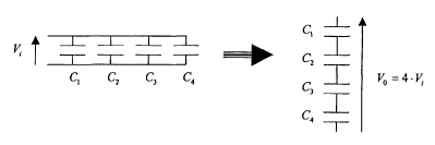
Figs. 1.1 and 1.2 show the basic concept of charge pumps: a circuit comprising
two
input terminals and a plurality of condensers C,, C2, C3, C4 series connected
with
the input terminals. All the condensers are charged at a voltage V; and subse-
quently the circuit is connected again so that the condensers are in parallel.
The
voltage in output terminals Vo is four times the voltage V. Furthermore, doing
the
sequence in a reverse way, it is possible to divide the voltage by four. In
these
schemes neither all the interconnection or the corresponding relays have been
CA 02564473 2006-10-20
WO 2005/111759 PCT/EP2005/005123
-8-
shown because a plurality of them must exist in order to allow all the
required con-
nections.
With this type of circuit it is possible to increase or reduce the output
voltage in a
discrete manner: as multiples of the input voltage or as divisions of the
input voltage
by an integer. Thus, a preferred solution of a regulator circuit according to
the in-
vention comprises voltage monitoring means of at least one of the condensers,
wherein these monitoring means are suitable for detecting the voltage
variation of
the condenser along time, and further comprises control means suitable for
discon-
necting the condenser from the input terminals when its voltage reaches a
prede-
termined value. In fact, in this manner it can be achieved that the condenser
(or
condensers) is charged with any voltage ranging from 0 and V;, whereby subse-
quently any voltage value at the output of the regulator circuit can be
achieved. An
example of monitoring and control means of this type are shown in Fig. 2.1.
The
relay S, has a resistance when it is connected that is represented by Rr. The
volt-
age in terminals Vo of the condenser C is compared with a reference voltage Vr
and
the relay is opened when Vo = Vr. If the input voltage has pick values higher
than
the feeding voltage of the comparator, it will be necessary to reduce the
voltage
arriving to the comparator, and that can be carried out for example placing a
resis-
tive voltage divider before the input negative terminal of the comparator,
with high
resistance values in order not to have remarkable energetic losses (Fig. 2.2).
Figs. 1.1. and 1.2 show reactance connection basic schemes. However, in order
to
obtain a higher accuracy in the output signal (without needing to use
monitoring
means) different strategies can be used:
- having two cascade regulator circuits, carrying out a first signal
amplification
and subsequently a reduction of it (or vice versa). The order will depend on
whether the output voltage must be high (in that case the first step will be
of re-
duction in order to avoid too high voltages) or on whether the output voltage
is
reduced, (in that case the first step will be of amplification in order to
avoid too
low voltages and noise problems).
CA 02564473 2006-10-20
WO 2005/111759 PCT/EP2005/005123
-9-
- having a plurality of parallel reactance batteries, wherein each battery is
formed
by a plurality of series reactances. All the reactances are simultaneously
charged and subsequently the reactances that must be connected to the output
in order to reach the desired signai are chosen. An example is shown in Fig. 3
wherein three batteries with four condensers each are shown. In this case, for
example, it is possible to amplify the input voltage V;n until a maximum of 3
V;n
times its value and in ranges of V;n/4.
The subject of the invention is also a power supply comprising a regulator
circuit
according to the invention, or, in other words, the use of a regulator circuit
accord-
ing to the invention for manufacturing a power supply.
The regulator circuit according to the invention preferably comprises at least
one of
the following additional elements:
a - a digital power supply module, that generates the necessary voltage in
order to
supply a digital circuitry comprised in the regulator circuit, and that
comprises a first
power supply having a first normally-on security relay in its first power
input termi-
nals, a second power supply having a second normally-off security relay in its
sec-
ond power input terminals, wherein the second relay is closed by means of the
volt-
age generated by the first power supply. The objective of this module is to
supply
the continuos current VDD necessary for the digital circuitry of the regulator
circuit.
Fig. 4.1 shows an example of digital power supply module and Figs. 4.2 to 4.5
show
an activation sequence. In order to simplify the schemes, in most part of the
follow-
ing diagrams neither the terminal or the corresponding connections to 0 V (or
earthing or ground) are represented. The relays R1 and R2 are normally-on
relays
and the relays R3 and R4 are normally-off relays. When all the regulator
circuit is
turned off, V;, = 0, and the situation shown in Fig. 4.2 occurs. The first
power sup-
ply is represented by VDDO and the second power supply is represented by VDD1.
When applying a voltage V;n , then VDDO rectifies this voltage and generates a
volt-
age VCC through its output that supplies the second power supply VDD1. The
first
thing that VDD1 does when it is activated, is to connect the relay R4 (Fig.
4.3). In
CA 02564473 2006-10-20
WO 2005/111759 PCT/EP2005/005123
-10-
this manner VDD1 receives the voltage V;, and can regulate it. Preferably the
first
power supply VDDO is a conventional lineal power supply and the second power
supply VDD1 comprises a second regulator circuit at least comprising two input
terminals, at least a first group of reactances with at least two reactances,
at least
two output terminals, a plurality of interconnections suitable for connecting
the re-
actances with respect to one another and suitable for connecting at least one
of the
reactances with the input and output terminals, wherein the interconnections
com-
prise miniaturised relays and wherein the miniaturised relays allow to
exchange a
series connection of said reactances for a parallel connection and vice versa.
I.e.,
preferably the second power supply VDD1 comprises a regulator circuit equal to
the
regulator circuit that it must supply. After activating the second power
supply VDD1,
a voltage VCC through the output VDD1 of VDD1 is obtained. At this moment, the
relay R2 is opened and the relay R3 is closed (Fig. 4.4). Finally the relay R1
opens,
whereby the first power supply VDDO is disconnected, and the activation
sequence
is finished (Fig. 4.5).
In general, in the present description and claims, the expressions "normally-
on re-
lay" and "normally-off relay" have been used as if they were a single relay.
How-
ever, there are different forms of designing these relays and in some of them
(as it
will be seen below) these relays are formed by a plurality of "elemental
relays".
Therefore, in the present description and claims it will be understood that
the ex-
pressions "normally-on relay" and "normally-off relay" refer to mechanisms
that can
be more or less complex, formed by a single physical relay or by several,
wherein
these mechanisms are capable of performing the functions of a normally-off
relay or
a normally-on relay.
b - an input protection module comprising a normally-off reiay that avoids
that over-
loads arrive to the reactances when the regulator circuit is turned off.
c - a rectifying module that rectifies an input signal connected to said input
termi-
nals. Preferably this rectifying module comprises miniaturised relays suitable
for
reversing the polarity of the input terminals in a dynamic fashion depending
on an
alternating signal connected to said input terminals that is the one wished to
be rec-
CA 02564473 2006-10-20
WO 2005/111759 PCT/EP2005/005123
-11-
tified. This solution is advantageous with respect to a solution based on a
bridge of
diodes given that it avoids both the voltage fall of them and the consequent
power
loss.
d - a reference signal module, that compares the signal in said input
terminals with
the signal in said output terminals and it sends a control signal to a signal
regulation
module. As it has been previously commented, in general, the regulator circuit
can
have coils and/or condensers. Thus the reference signal module can be likewise
a
module operating with voltages or currents. In general, this module will have
two
to input signals: the reference signal and the actual output signal of the
regulator cir-
cuit, and an output signal that will be responsible for adjusting the actual
value to
the reference value. Optionaily, this reference signal module can include an
oscil-
lator so that the regulator circuit will generate an alternating current
signal. That
would allow, to obtain alternating current from any continuous current source,
such
as for example of the battery of a vehicle.
e - an output module comprising an output filter with an output condenser
that, as
previously commented, allows supplying to the charge a more uniform voltage.
f - an output protection module with a normally-off security relay, so that in
the case
of an overload at the output said relay opens and disconnects said regulator
circuit
from said output terminals.
These additional modules are particularly interesting if the regulator circuit
is incor-
porated in a power supply, although several of these modules can be used in
the
other devices that are the subject of this invention, as it is clear for an
expert in the
art.
Another preferred use of a regulator circuit according to the invention is for
manu-
facturing an A/D (analogue/digital) converter. Or, in other words, the subject
of the
invention is also an analogue/digital converter comprising a regulator circuit
ac-
cording to the invention. In this sense it is advantageous that the regulator
circuit
according to the invention comprises an A/D converter connected to the output
ter-
CA 02564473 2006-10-20
WO 2005/111759 PCT/EP2005/005123
-12-
minals. In fact the regulator circuit amplifies the signal before being
digitilized. Only
by means of a regulator circuit according to the invention it is possible to
amplify the
signal highly above the supply voltage, as the conventional active amplifiers
are not
capable of it. In this manner it is achieved to minimise the effect of the
noise intro-
duced during the digitalization, given that a signal of a much higher value
and that
has been amplified by a device further generating very little noise is being
digitilized.
Therefore, if the resolution that can be obtained by the system is of OV, as
the sig-
nal has been amplified without affecting the AV, the final resolution will be
higher.
Advantageously the A/D converter comprises a segmented converter comprising a
first voltage divider with G impedances, G comparator devices connected
between
said output signal and said voltage divider, comprising each of said
comparator de-
vices a second voltage divider with G impedances and a comparator, and a
second
A/D converter. Indeed, a possible drawback of the above A/D converter is that
it
must convert a signal that possibly has a much higher voltage than the supply
volt-
age of the circuit, and that can be a problem for conventional A/D converters.
A way
of solving this drawback is by replacing the conventional A/D converter by a
RC
circuit and a discharge time meter. However this system is not very accurate.
The
segmented converter allows, however, to obtain a very high resolution.
An example of this segmented converter can be seen in Fig. 5. The segmented
converter has an input voltage G V;n (that, in fact, will be the output
voltage in the
regulator circuit terminals) that is G times the original voltage to be
digitilized. I.e.,
the regulator circuit has amplified the original signal by a factor of G. Then
the seg-
mented converter divides the reference voltage G=Vcc by the first voltage
divider
(having G impedances), and compares the signal G=V;n with the voltage of each
of
the segments of the first voltage divider in the corresponding comparator
device
CDU. In the example of Fig. 5 the segmented converter has four comparator de-
vices (G=4) indicated with CDU1, CDU2, CDU3, and CDU4. In this manner it can
determine within which voltage segment is G=V;n. In this manner the more
significant
bits of the digitilized signal V;, are determined. Finally, the signal
corresponding to
the "border" segment is taken, it is divided by G through a second voltage
divider
included in each comparator device CDU and it is sent to a second A/D
converter
CA 02564473 2006-10-20
WO 2005/111759 PCT/EP2005/005123
-13-
ADC, that can be conventional. This second A/D converter ADC will be
responsible
for the less significant bits of the digitilized signal.
In Fig. 6.1 it is observed that a comparator device CDU and in Figs. 6.2 to
6.4 its
comparation sequence. The comparator device CDU firstly connects its voltage
divider (the second voltage divider that each comparator device has, and that
is
formed in this example by four series condensers) to the voltage corresponding
to
the first voltage divider VREF;, on the one hand, and to G=V;n, on the other
hand
(Fig. 6.2). As it can be seen, the voltage drop in terminals of the second
voltage
divider will be different for each comparator device CDU as VREF; is different
for
each comparator device CDU, so that for some it will be a negative voltage
whilst
for others it will be a positive voltage. Then it is detected whether said
voltage dif-
ference is positive or negative by connecting the terminals of one of the
condensers
(we will have VC;, i.e. the voltage difference divided by 4, so ensuring that
we are
always within the operating range of the used electronics) to a comparator
that will
give a C;, signal indicative of the sign of the voltage difference (Fig. 6.3).
Knowing in
which comparator device the sign change takes place, it is already possible to
de-
termine the most important bits of the digital signal. Finally (Fig. 6.4) the
voltage is
connected in the terminals of one of the condensers (of the same that has
served
for detecting the change of the voltage sign or of another condenser of the
second
voltage divider) to the terminals ADCL and ADCH of a conventional A/D
converter,
that will determine the less important bits of the digital signal.
Another preferred use of a regulator circuit according to the invention is for
manu-
facturing a D/A (digital/analogue) converter. Or, in other words, the subject
of the
invention is also a D/A (digital/analogue) converter that comprises a
regulator circuit
according to the invention. In this sense it is advantageous that the
regulator circuit
according to the invention comprises a D/A converter connected to its input
termi-
nals. An example of a D/A converter according to the invention is shown in
Fig. 7. In
this example the regulator circuit has four condensers that can be
independently
connected to Vcc, to GND, or to an output of a conventional D/A converter
DACO.
Furthermore it is possible to connect the four condensers in series. If one
supposes,
by way of example, that Vcc is 5V then the maximum value at the output of the
four
CA 02564473 2006-10-20
WO 2005/111759 PCT/EP2005/005123
-14-
condensers connected in series will be of 20V, that is, the signal has been
amplified
four times. If the digitalized signal corresponds to 3V (i.e., 3/5 of the
reference
value), then the output voltage of the condensers connected in series will
have to be
of 12V. A digital circuitry, properly programmed, carries out these
calculations and
performs the following actions:
- it activates the corresponding relays in order that the lower two relays are
con-
nected to Vcc (5V + 5V = 10V), in parallel with respect to one another,
- it sends the corresponding digital value in order that the D/A converter
DACO gen-
erates a voltage of 2V,
- it activates the relay of the third condenser in order to connect it to the
DIA con-
verter DACO (10V + 2V = 12V),
- it activates the relay of the fourth condenser in order to connect it to
GND.
Once the condensers are charged, they are connected in series and the voltage
of
12V is obtained (corresponding to 3/5 of the reference value that now is of
20V).
In this manner a D/A converter of more accurateness, less cost and faster, in
par-
ticular in the case of high accuracies is achieved.
Preferably the regulator circuit (that is part of the D/A converter) comprises
a sec-
ond regulator circuit that at least comprises two input terminals, at least a
first group
of reactances with at least two reactances, at least two output terminals, a
plurality
of interconnections suitable for connecting the reactances with respect to one
an-
other and suitable for connecting at least one of the reactances with the
input and
output terminals, wherein the interconnections comprise miniaturised relays
and
wherein the miniaturised relays allow to exchange a series connection of the
reac-
tances for a parallel connection and vice versa, wherein this second regulator
circuit
is connected to the output terminals of the first regulator circuit. Indeed,
this second
regulator circuit is shown in Fig. 7 as the amplifier =4. Its function is to
adjust again
the signal to the reference value Vcc, so that, following the previous
example, the
value of Vo would finally be the 3V that were wished to obtain.
CA 02564473 2006-10-20
WO 2005/111759 PCT/EP2005/005123
-15-
Advantageously the regulator circuit (that is part of the D/A converter)
comprises an
output buffer and/or a track and hold amplifier. That allows to disengage the
reac-
tances of the charge applied to the D/A converter and to maintain the signal
gener-
ated during some time. Alternatively according to the invention several D/A
convert-
ers connected in parallel could be used so that they are sequentially
connected to
the charge.
The subject of the invention is also the use of a regulator circuit according
to the
invention to manufacture a power amplifier, i.e., the invention also relates
to power
1o amplifiers comprising a regulator circuit according to the invention.
The invention further relates to a regulator circuit comprising one (or
several)
miniaturised relay particularly suitable for the above applications.
Currently there are various alternatives for the production of miniaturised
relays, in
particular, in the context of technologies known as MEMS technology (micro
electro-
mechanical), Microsystems and/or Micromachines. In principal such may be
classi-
fied according to the type of force or actuation mechanism they use to move
the
contact electrode. The classification usually applied is thus between
electrostatic,
magnetic, thermal and piezoelectric relays. Each one has its advantages and
its
drawbacks. However miniaturisation techniques require the use of activation
volt-
ages and surfaces which are as small as possible. Relays known in the state of
the
art have several problems impeding their advance in this respect.
A manner of reducing the activation voltage is precisely to increase the relay
sur-
face areas, which renders miniaturisation difficult, apart from being
conducive to the
appearance of deformations reducing the useful life and reliability of the
relay. In
electrostatic relays, another solution for decreasing the activation voltage
is to
greatly reduce the space between the electrodes, or use very thin electrodes
or
special materials, so that the mechanical recovery force is very low. However
this
implies problems of sticking, since capillary forces are very high, which thus
also
reduces the useful working life and reliability of these relays. The use of
high acti-
vation voltages also has negative effects such as ionisation of the
components, ac-
CA 02564473 2006-10-20
WO 2005/111759 PCT/EP2005/005123
-16-
celerated wearing due to strong mechanical solicitation and the electric noise
which
the relay generates.
Electrostatic relays also have a significant problem as to reliability, due to
the phe-
nomenon known as "pull-in", and which consists in that, once a given threshold
has
been passed, the contact electrode moves in increasing acceleration against
the
other free electrode. This is due to the fact that as the relay closes, the
condenser
which exerts the electrostatic force for closing, greatly increases its
capacity (and
would increase to infinity if a stop were not imposed beforehand).
Consequently
there is a significant wear on the electrodes due to the high electric field
which is
generated and the impact caused by the acceleration to which the moving
electrode
has been exposed.
Thermal, magnetic and piezoelectric approaches require special materials and
mi-
cromachined processes, and thus integration in more complex MEMS devices, or
in
a same integrated with electronic circuitry is difficult and/or costly.
Additionally the
thermal approach is very slow (which is to say that the circuit has a long
opening or
closing time) and uses a great deal of power. The magnetic approach generates
electromagnetic noise, which renders having close electronic circuitry much
more
difficult, and requires high peak currents for switching.
In the present description and claims the expression "contact point" has been
used
to refer to contact surfaces in which an electric contact is made (or can be
made).
In this respect, they should not be understood as points in the geometric
sense,
since they are three-dimensional elements, but rather in the electric sense,
as
points in an electric circuit.
Thus the invention has another preferred embodiment by which at least one of
the
miniaturised relays of the regulator circuit comprises:
- a first zone facing a second zone,
- a first condenser plate,
- a second condenser plate arranged in the second zone, in which the second
plate
is smaller than or equal to the first plate,
CA 02564473 2006-10-20
WO 2005/111759 PCT/EP2005/005123
-17-
- an intermediate space arranged between the first zone and the second zone,
- a conductive element arranged in the intermediate space, the conductive
element
being mechanically independent of the first zone and the second zone and being
suitable for performing a movement across the intermediate space dependant on
voltages present in the first and second condenser plates,
- a first contact point of an electric circuit, a second contact point of the
electric cir-
cuit, in which the first and second contact point define first stops, in which
the con-
ductive element is suitable for entering into contact with the first stops and
in which
the conductive element closes the electric circuit when in contact with the
first stops.
In fact in the relay according to the invention the conductive element, which
is to say
the element responsible for opening and closing the external electric circuit
(across
the first contact point and the second contact point), is a detached part
capable of
moving freely. I.e. the elastic force of the material is not being used to
force one of
the relay movements. This allows a plurality of different solutions, all
benefiting
from the advantage of needing very low activation voltages and allowing very
small
design sizes. The conductive element is housed in the intermediate space. The
intermediate space is closed by the first and second zone and by lateral walls
which
prevent the conductive element from leaving the intermediate space. When
voltage
is applied to the first and second condenser plate charge distributions are
induced
in the conductive element which generates electrostatic forces which in turn
move
the conductive element in a direction along the intermediate space. By means
of
different designs to be described in detail below this effect can be used in
several
different ways.
Additionally, a relay according to the invention likewise satisfactorily
resolves the
previously mentioned problem of "pull-in".
Another additional advantage of the relay according to the invention is the
following:
in conventional electrostatic relays, if the conductive element sticks in a
given posi-
tion (which depends to a great extent, among other factors, on the humidity)
there is
no possible manner of unsticking it (except by external means, such as for
example
drying it) since due to the fact that the recovery force is elastic, is always
the same
CA 02564473 2006-10-20
WO 2005/111759 PCT/EP2005/005123
-18-
(depending only on the position) and cannot be increased. On the contrary, if
the
conductive element sticks in a relay according to the invention, it will
always be pos-
sible to unstick it by increasing the voltage.
The function of the geometry of the intermediate space and the positioning of
the
condenser plates can furnish several different types of relays, with as many
appli-
cations and functioning methods.
For example, the movement of the conductive element can be as follows:
- a first possibility is that the conductive element moves along the
intermediate
space with a movement of translation, i.e., in a substantially rectilinear
manner (ex-
cluding of course possible impacts or oscillations and/or movements provoked
by
unplanned and undesired external forces) between the first and second zones.
- a second possibility is that the conductive element have a substantially
fixed end,
around which can rotate the conductive element. The rotational axis can serve
the
function of contact point for the external electric circuit and the free end
of the con-
ductive element can move between the first and second zones and make, or not
make, contact with the other contact point, depending on its position. As will
be
outlined below, this approach has a range of specific advantages.
Advantageously the first contact point is between the second zone and the
conduc-
tive element. This allows a range of solutions to be obtained, discussed
below.
A preferable embodiment is achieved when the first plate is in the second
zone.
Alternatively the relay can be designed so that the first plate is in the
first zone. In
the first case a relay is obtained which has a greater activation voltage and
which is
faster. On the other hand, in the second case the relay is slower, which means
that
the shocks experienced by the conductive element and the stops are smoother,
and
energy consumption is lower. One can obviously choose between one or the other
alternatives depending on the specific requirements in each case.
CA 02564473 2006-10-20
WO 2005/111759 PCT/EP2005/005123
-19-
A preferable embodiment of the invention is obtained when the second contact
point
is likewise in the second zone. In this case one will have a relay in which
the con-
ductive element performs the substantially rectilinear translation movement.
When
the conductive element is in contact with the first stops, which is to say
with the first
and second contact point of the electric circuit, the electric circuit is
closed, and it is
possible to open the electric circuit by means of different types of forces,
detailed
below. To again close the electric circuit, it is enough to apply voltage
between the
first and second condenser plates. This causes the conductive element to be at-
tracted toward the second zone, again contacting the first and second contact
point.
Should the first condenser plate be in the first zone and the second condenser
plate
in the second zone, a manner of achieving the necessary force to open the
circuit
cited in the above paragraph is by means of the addition of a third condenser
plate
arranged in the second zone, in which the third condenser plate is smaller
than or
equal to the first condenser plate, and in which the second and third
condenser
plates are, together, larger than the first condenser plate. With this
arrangement
the first condenser plate is to one side of the intermediate space and the
second
and third condenser plates are to the other side of the intermediate space and
close
to one another. In this manner one can force the movement of the conductive
ele-
.20 ment in both directions by means of electrostatic forces and, in addition,
one can
guarantee the closing of the external electric circuit even though the
conductor ele-
ment remains at a voltage in principle unknown, which will be forced by the
external
circuit that is closed.
Another preferable embodiment of the invention is achieved when the relay addi-
tionally comprises a third condenser plate arranged in said second zone and a
fourth condenser plate arranged in said first zone, in which said first
condenser
plate and said second condenser plate are equal to each other, and said third
con-
denser plate and said fourth condenser plate are equal to one another. In
fact, in
this manner, if one wishes the conductive element to travel towards the second
zone, one can apply voltage to the first and fourth condenser plates, on one
side,
and to the second or to the third condenser plates, on the other side. Given
that the
conductive element will move toward the place in which is located the smallest
con-
CA 02564473 2006-10-20
WO 2005/111759 PCT/EP2005/005123
-20-
denser plate, it will move toward the second zone. Likewise one can obtain
move-
ment of the conductive element toward the first zone by applying a voltage to
the
second and third condenser plates and to the first or the fourth condenser
plates.
The advantage of this solution, over the simpler three condenser plate
solution, is
that it is totally symmetrical, which is to say that it achieves exactly the
same relay
behaviour irrespective of whether the conductive element moves toward the
second
zone or the first zone. Advantageously the first, second, third and fourth
condenser
plates are all equal with respect to one another, since generally it is
convenient that
in its design the relay be symmetrical in several respects. On one hand there
is
io symmetry between the first and second zone, as commented above. On the
other
hand it is necessary to retain other types of symmetry to avoid other
problems, such
as for example the problems of rotation or swinging in the conductive element
and
which will be commented upon below. In this respect it is particularly
advantageous
that the relay comprise, additionally, a fifth condenser plate arranged in the
first
zone and a sixth condenser plate arranged in the second zone, in which the
fifth
condenser plate and the sixth condenser plate are equal to each other. On one
hand increasing the number of condenser plates has the advantage of better com-
pensating manufacturing variations. On the other, the several different plates
can
be activated independently, both from the point of view of voltage applied as
of acti-
vation time. The six condenser plates can all be equal to each other, or
alterna-
tively the three plates of a same side can have different sizes with respect
to one
another. This allows minimising activation voltages. A relay which has three
or
more condenser plates in each zone allows the following objectives to all be
achieved:
- it can function in both directions symmetrically,
- it has a design which allows a minimum activation voltage for fixed overall
relay
dimensions, since by having two plates active in one zone and one plate active
in
the other zone distinct surface areas can always be provided,
- it allows minimisation of current and power consumption, and also a smoother
relay functioning,
CA 02564473 2006-10-20
WO 2005/111759 PCT/EP2005/005123
-21 -
- it can guarantee the opening and closing of the relay, independently of the
voltage
transmitted by the external electric circuit to the conductive element when
they enter
in contact,
- in particular if the relay has six condenser plates in each zone, it can in
addition
comply with the requirement of central symmetry which, as we shall see below,
is
another significant advantage. Therefore another preferable embodiment of the
invention is obtained when the relay comprises six condenser plates arranged
in the
first zone and six condenser plates arranged in the second zone. However it is
not
absolutely necessary to have six condenser plates in each zone to achieve
central
1o symmetry: it is possible to achieve it as well, for example, with three
condenser
plates in each zone, although in this case one must forego minimising current
and
power consumption and optimising the "smooth" functioning of the relay. In gen-
eral, increasing the number of condenser plates in each zone allows greater
flexibil-
ity and versatility in the design, whilst it allows a reduction of the
variations inherent
in manufacture, since the manufacturing variations of each of the plates will
tend to
be compensated by the variations of the remaining plates.
However it should not be discounted that in certain cases it can be
interesting to
deliberately provoke the existence of force moments in order to force the
conductive
2o element to perform some kind of revolution additional to the translation
movement.
It could be advantageous, for example, to overcome possible sticking or
friction of
the conductive element with respect to the fixed walls.
Advantageously the relay comprises a second stop (or as many second stops as
there are first stops) between the first zone and the conductive element. In
this
manner one also achieves a geometric symmetry between the first zone and the
second zone. When the conductive element moves toward the second zone, it can
do so until entering into contact with the first stops, and will close the
external elec-
tric circuit. When the conductive element moves toward the first zone it can
do so
until entering into contact with the second stop(s). In this manner the
movement
performed by the conductive element is symmetrical.
CA 02564473 2006-10-20
WO 2005/111759 PCT/EP2005/005123
-22-
Another preferable embodiment of the invention is achieved when the relay com-
prises a third contact point arranged between the first zone and the
conductive ele-
ment, in which the third contact point defines a second stop, such that the
conduc-
tive element closes a second electric circuit when in contact with the second
contact
point and third contact point. In this case the relay acts as a commuter,
alternately
connecting the second contact point with the first contact point and with the
third
contact point.
A particularly advantageous embodiment of the previous example is achieved
when
1o the conductive element comprises a hollow cylindrical part which defines a
axis, in
the interior of which is housed the second contact point, and a flat part
which pro-
trudes from one side of the radially hollow cyiindrical part and which extends
in the
direction of the axis, in which the flat part has a height, measured in the
direction of
the axis, which is less than the height of the cylindrical part, measured in
the direc-
tion of the axis. This specific case complies simultaneously with the
circumstance
that the conductive element perform a rotational movement around one of its
ends
(cf. the "second possibility" cited above). Additionally, the cylindrical part
is that
which rests on bearing surfaces (one at each end of the cylinder, and which
extends
between the first zone and the second zone) whilst the flat part is
cantilevered with
respect to the cylindrical part, since it has a lesser height. Thus the flat
part is not in
contact with walls or fixed surfaces (except the first and third contact
point) and, in
this manner, the sticking and frictional forces are lessened. As to the second
point
of contact, it is housed in the internal part of the cylindrical part, and
serves as rota-
tional axis as well as second contact point. Thus an electric connection is
estab-
lished between the first and second contact points or between the third and
second
contact points. The hollow cylindrical part defines a cylindrical hollow,
which in a11
cases has a surface curved to the second contact point, thus reducing the
risks of
sticking and frictional forces.
Another particularly advantageous embodiment of the previous example is
obtained
when the conductive element comprises a hollow parallelepipedic part which
defines
a axis, in the interior of which is housed the second contact point, and a
flat part
which protrudes from one side of the radially hollow paralelepipedic part and
which
CA 02564473 2006-10-20
WO 2005/111759 PCT/EP2005/005123
-23-
extends in the direction of the axis, in which the flat part has a height,
measured in
the direction of the axis, which is less than the height of the
parallelepipedic part,
measured in the direction of the axis. In fact, it is an embodiment similar to
that
above, in which the parallelepipedic part defines a parallelepipedic hollow.
This
solution can be particularly advantageous in the case of very small
embodiments,
since in this case the resolution capacity of the manufacturing process (in
particular
in the case of the photolithographic procedures) obliges the use of straight
lines. In
both cases it should be emphasised that the determining geometry is the
geometry
of the interior hollow and that, in fact, several different combinations are
possible:
- axis (second contact point) having a rectangular section and hollow with
rectan-
gular section,
- axis having a circular section and hollow having a circular section
- axis having a circular section and hollow having a rectangular section, and
vice
versa
although the first two combinations are the most advantageous.
Logically, should the sections be rectangular, there should be enough play
between
the axis and the parallelepipedic part such that the conductive element can
rotate
around the axis. Likewise in the case of circular sections there can be a
significant
amount of play between the axis and the cylindrical part, such that the real
move-
ment performed by the conductive element is a combination of rotation around
the
axis and translation between the first and second zone. It should be noted,
addi-
tionally, that it is also possible that the second stop not be connected
electrically to
any electric circuit: in this case a relay will be obtained which can open and
close
only one electric circuit, but in which the conductive element moves by means
of a
rotation (or by means of a rotation combined with translation).
Another preferable embodiment of the invention is obtained when the relay com-
prises a third and a fourth contact points arranged between the first zone and
the
conductive element, in which the third and fourth contact points define second
stops, such that the conductive element closes a second electric circuit when
in
CA 02564473 2006-10-20
WO 2005/111759 PCT/EP2005/005123
-24-
contact with the third and fourth contact points. In fact, in this case the
relay can
alternatively connect two electric circuits.
Advantageously each of the assemblies of condenser plates arranged in each of
the
first zone and second zone is centrally symmetrical with respect to a centre
of
symmetry, in which said centre of symmetry is superposed to the centre of
masses
of the conductive element. In fact, each assembly of the condenser plates
arranged
in each of the zones generates a field of forces on the conductive element. If
the
force resulting from this field of forces has a non nil moment with respect to
the
centre of masses of the conductive element, the conductive element will not
only
undergo translation but will also undergo rotation around its centre of
masses. In
this respect it is suitable to provide that the assemblies of plates of each
zone have
central symmetry in the case that this rotation is not advantageous, or on the
other
hand it could be convenient to provide central asymmetry should it be
advantageous
to induce rotation in the conductive element with respect to its centre of
masses, for
example to overcome frictional forces and/or sticking.
As already indicated, the conductive element is usually physically enclosed in
the
intermediate space, between the first zone, the second zone and lateral walls.
Ad-
vantageously between the lateral walls and the conductive element there is
play
sufficiently small such as to geometrically prevent the conductive element
entering
into contact simultaneously with a contact point of the group formed by the
first and
second contact points and with a contact point of the group formed by the
third and
fourth contact points. That is to say, the conductive element is prevented
from
adopting a transversal position in the intermediate space in which it connects
the
first electric circuit to the second electric circuit.
To avoid sticking and high frictional forces it is advantageous that the
conductive
element has rounded external surfaces, preferably that it be cylindrical or
spherical.
The spherical solution minimises the frictional forces and sticking in all
directions,
whilst the cylindrical solution, with the bases of the cylinder facing the
first and sec-
ond zone allow reduced frictional forces to be achieved with respect to the
lateral
walls whilst having large surfaces facing the condenser plates - efficient as
con-
CA 02564473 2006-10-20
WO 2005/111759 PCT/EP2005/005123
-25-
cerns generation of electrostatic forces. This second solution also has larger
con-
tact surfaces with the contact points, diminishing the electric resistance
which is
introduced in the commuted electric circuit.
Likewise, should the conductive element have an upper face and a lower face,
which are perpendicular to the movement of the conductive element, and at
least
one lateral face, it is advantageous that the lateral face has slight
protuberances.
These protuberances will further allow reduction of sticking and frictional
forces
between the lateral face and the lateral walls of the intermediate space.
Advantageously the conductive element is hollow. This allows reduced mass and
thus achieves lower inertia.
Should the relay have two condenser plates (the first plate and the second
plate)
and both in the second zone, it is advantageous that the first condenser plate
and
the second condenser plate have the same surface area, since in this manner
the
minimal activation voltage is obtained for a same total. device surface area.
Should the relay have two condenser plates (the first plate and the second
plate)
and the first plate is in the first zone whilst the second plate is in the
second zone, it
is advantageous that the first condenser plate has a surface area that is
equal to
double the surface area of the second condenser plate, since in this manner
the
minimal activation voltage is obtained for a same total device surface area.
Another preferable embodiment of a relay according to the invention is
obtained
when one of the condenser plates simultaneously serves as condenser plate and
as
contact point (and thus of stop). This arrangement will allow connection of
the other
contact point (that of the external electric circuit) at a fixed voltage
(normally VCC or
GND) or leaving it at high impedance.
Usually the relay will be opened and closed by voltages applied to the plates
of the
condensers. However it is possible to make one of the 'movements by another
physical magnitude. In such cases, the physical magnitude exerts a force to
open
CA 02564473 2006-10-20
WO 2005/111759 PCT/EP2005/005123
-26-
the electric circuit and by means of a given voltage applied to the condenser
plates
a force is generated which counteracts the former and the external electric
circuit is
again closed (or vice versa, i.e., it is necessary to apply a voltage to
maintain the
electric circuit open whilst the physical magnitude which one wishes to study
tends
to close the circuit). Examples of these physical magnitudes can be
accelerations,
pressures, flows, etc.
As can be observed below, the preferred embodiments of the invention shown in
the Figs. include a combination of several alternatives and options previously
ex-
io plained, although an expert in the art will be able to see that they are
alternatives
and options that can be mutually combined in different ways.
Fig. 8 shows a first basic functioning mode of a relay according to the
invention.
The relay defines an intermediate space 25 in which is housed a conductive ele-
ment 7, which can move freely along the intermediate space 25, since
physically it
is a detached part which is not physically joined to the walls which define
the inter-
mediate space 25. The relay also defines a first zone, on the left in figure
8, and a
second zone, on the right in figure 8. In the second zone are arranged a first
con-
denser plate 3 and a second condenser plate 9. In the example shown in figure
8
both condenser plates 3 and 9 have different surface areas, although they can
be
equal with respect to one another. The first condenser plate 3 and the second
con-
denser plate 9 are connected to a CC control circuit. Applying a voltage
between
the first condenser plate 3 and the second condenser plate 9, the conductive
ele-
ment is always attracted towards the right in figure 1, towards the condenser
plates
3 and 9. The conductive element 7 will be moved towards the right until being
stopped by first stops 13, which are a first contact point 15 and a second
contact
point 17 of a first external electric circuit CE1, such that the first
external electric
circuit CE1 is closed.
Fig. 9 shows a second basic functioning mode for a relay according to the
invention.
The relay again defines an intermediate space 25 in which is housed a
conductive
element 7, which can move freely along the intermediate space 25, a first
zone, on
the left in figure 2, and a second zone, on the right in figure 9. In the
second zone
CA 02564473 2006-10-20
WO 2005/111759 PCT/EP2005/005123
-27-
is arranged a second condenser plate 9 whilst in the first zone is arranged a
first
condenser plate 3. The first condenser plate 3 and the second condenser plate
9
are connected to a CC control circuit. Applying a voltage between the first
con-
denser plate 3 and the second condenser plate 9, the conductive element is
always
attracted to the right of the figure 9, towards the smallest condenser plate,
i.e. to-
wards the second condenser plate 9. For this reason, the fact that in the
example
shown in figure 2 both condenser plates 3 and 9 have different surface areas
is, in
this case, absolutely necessary, since if they were to have equal surface
areas, the
conductive element 7 would not move in any direction. The conductive element 7
io will move towards the right until being stopped by first stops 13, which
are a first
contact point 15 and a second contact point 17 of a first external electric
circuit
CE1, such that the first external electric circuit CE1 is closed. On the left
there are
second stops 19 which in this case do not serve any electric function but
which stop
the conductive element 7 from entering into contact with the first condenser
plate 3.
In this case the stops 19 can be removed, since no problem is posed by the con-
ductive element 7 entering into contact with the first condenser plate 3. This
is be-
cause there is only one condenser plate on this side, if there had been more
than
one and if they had been connected to different voltages then the stops would
have
been necessary to avoid a short-circuit.
The configurations of the relays of figures 8 and 9 are suitable for being
used as
sensors, in which the magnitude to be measured exercises a force which is that
which will be counteracted by the electrostatic force induced in the
conductive ele-
ment 7, although they could be used as relays as long as there is an external
force
(acceleration, pressure, etc.) capable of moving the conductive element 7.
Such as
represented, in both cases the magnitude to be measured must exercise a force
tending to open the electric circuit CE1, whilst the electrostatic force will
tend to
close it. However, a relay can be designed to work exactly in the opposite
respect:
such that the magnitude to be measured would tend to close the electric
circuit CE1
whilst the electrostatic force would tend to open it. In this case, the first
stops 13
would need to be positioned on the left in figures 8 and 9, together with the
corre-
sponding electric circuit CE1. In figure 8 this possibility has been shown in
a broken
line.
CA 02564473 2006-10-20
WO 2005/111759 PCT/EP2005/005123
-28-
To achieve moving the conductive element 7 in both directions by means of
electro-
static forces, it is necessary to provide a third condenser plate 11, as shown
in fig-
ure 10. Given that the conductive element 7 will always move towards where the
smallest condenser plate is located, it is necessary, in this case, that the
third con-
denser plate 11 be smaller than the first condenser plate 3, but that the sum
of the
surface areas of the second condenser plate 9 and the third condenser plate 11
be
larger than the first condenser plate 3. In this manner, activating the first
condenser
plate 3 and the second condenser plate 9, connecting them to different
voltages,
but not the third condenser plate 11, which will remain in a state of high
impedance,
the conductive element 7 can be moved to the right, whilst activating the
three con-
denser plates 3, 9 and 11 the conductor element 7 can be moved to the left. In
the
latter case the second condenser plate 9 and the third condenser plate 11 are
sup-
plied at a same voltage, and the first condenser plate 3 at a different
voltage. The
relay of figure 10 has, in addition, a second external electric circuit CE2
connected
to the second stops 19, in a manner that these second stops 19 define a third
con-
tact point 21 and a fourth contact point 23.
Should two condenser plates be provided in each of the first and second zones,
the
movement of the conductive element 7 can be solicited in two different ways:
- applying a voltage between the two condenser plates of a same zone, so that
the
conductive element is attracted by them (functioning as in figure 8)
- applying a voltage between one condenser plate of one zone and a (or both)
con-
denser plate(s) of the other zone, such that the conductive element 7 is
attracted
towards the zone in which the electrically charged condenser surface area is
small-
est (functioning as in figure 9).
Figures 11 and 12 illustrate a relay designed to be manufactured with EFAB
tech-
nology. This micromechanism manufacturing technology by means of layer depos-
iting is known by persons skilled in the art, and allows the production of
several lay-
ers and presents a great deal of versatility in the design of three-
dimensional struc-
CA 02564473 2006-10-20
WO 2005/111759 PCT/EP2005/005123
-29-
tures. The relay is mounted on a substrate 1 which serves as support, and
which in
several of the appended drawings has not been illustrated in the interest of
simplic-
ity. The relay has a first condenser plate 3 and a fourth condenser plate 5
arranged
on the left (according to figure 12) of a conductive element 7, and a second
con-
denser plate 9 and a third condenser plate 11 arranged on the right of the
conduc-
tive element 7. The relay also has two first stops 13 which are the first
contact point
and the second contact point 17, and two second stops 19 which are the third
contact point 21 and the fourth contact point 23. The relay is covered in its
upper
part, although this cover has not been shown in order to be able to clearly
note the
1o interior details.
The relay goes from left to right, and vice versa, according to figure 12,
along the
intermediate space 25. As can be observed the first stops 13 and the second
stops
19 are closer to the conductive element 7 than the condenser plates 3, 5, 9
and 11.
15 In this manner the conductive element 7 can move from left to right,
closing the cor-
responding electric circuits, without interfering with the condenser plates 3,
5, 9 and
11, and their corresponding control circuits.
The conductive element 7 has a hollow internal space 27.
There is play between the conductive element 7 and the walls which form the
inter-
mediate space 25 (which is to say the first stops 13, the second stops 19, the
con-
denser plates 3, 5, 9 and 11 and the two lateral walls 29) which is
sufficiently small
to prevent the conductive element 7 from spinning along an axis perpendicular
to
the plane of the drawing of figure 12 enough to contact the first contact
point 15
with the third contact point 21 or the second contact point 17 with the fourth
contact
point 23. In the figures, however, the play is not drawn to scale, so as to
allow
greater clarity in the figures.
Figures 13 to 15 show another relay designed to be manufactured with EFAB tech-
nology. In this case the conductive element 7 moves vertically, in accordance
with
figures 13 to 15. The use of one or the other movement alternative in the
relay de-
pends on design criteria. The manufacturing technology consists in the deposit
of
CA 02564473 2006-10-20
WO 2005/111759 PCT/EP2005/005123
-30-
several layers. In all figures the vertical dimensions are exaggerated, which
is to
say that the physical devices are much flatter than as shown in the figures.
Should
one wish to obtain larger condenser surfaces it would be preferable to
construct the
relay with a form similar to that shown in the figures 13 to 15 (vertical
relay), whilst a
relay with a form similar to that shown in figures 11 and 12 (horizontal
relay) would
be more appropriate should a lesser number of layers be desired. Should
certain
specific technologies be used (such as those usually known as polyMUMPS,
Dalsa,
SUMMIT, Tronic's, Qinetiq's, etc) the number of layers will always be limited.
The
advantage of a vertical relay is that larger surfaces are obtained with a
smaller chip
area, and this implies much lower activation voltages (using the same chip
area).
Conceptually the relay of figures 13 to 15 is very similar to the relay of
figures 11
and 12, and has the first condenser plate 3 and the fourth condenser plate 5
ar-
ranged in the lower part (figure 15) as well as the second stops 19 which are
the
third contact point 21 and the fourth contact point 23. As can be seen in the
draw-
ings the second stops 19 are above the condenser plates, such that the
conductive
element 7 can bear on the second stops 19 without entering into contact with
the
first and fourth condenser plates 3, 5. In the upper end (figure 13) is the
second
condenser plate 9, the third condenser plate 11 and two first stops 13 which
are the
first contact point 15 and the second contact point 17. In this case the play
between
the conductive element 7 and the lateral walls 29 is also sufficiently small
to avoid
the first contact point 15 contacting with the third contact point 21 or the
second
contact point 17 contacting with the fourth contact point 23.
The relay shown in figures 16 and 17 is an example of a relay in which the
move-
ment of the conductive element 7 is substantially a rotation around one of its
ends.
This relay has a first condenser plate 3, a second condenser plate 9, a third
con-
denser plate 11 and a fourth condenser plate 5, all mounted on a substrate 1.
Ad-
ditionally there is a first contact point 15 and a third contact point 21
facing each
other. The distance between the first contact point 15 and the third contact
point 21
is less than the distance between the condenser plates. The conductive element
7
has a cylindrical part 31 which is hollow, in which the hollow is likewise
cylindrical.
CA 02564473 2006-10-20
WO 2005/111759 PCT/EP2005/005123
-31-
In the interior of the cylindrical hollow is housed a second contact point 17,
having a
cylindrical section.
In this manner the conductive element 7 will establish an electrical contact
between
the first contact point 15 and the second contact point 17 or the third
contact point
21 and the second contact point 17. The movement performed by the conductive
element 7 is substantially a rotation around the axis defined by the
cylindrical part
31. The play between the second contact point 17 and the cylindrical part 31
is ex-
aggerated in the figure 16, however it is certain that a certain amount of
play exists,
the movement performed by the conductive element 7 thus not being a pure
rotation
but really a combination of rotation and translation.
From the cylindrical part 31 extends a flat part 33 which has a lesser height
than the
cylindrical part 31, measured in the direction of the axis of said cylindrical
part 31.
This can be observed in greater detail in figure 17, in which is shown a view
almost
in profile of the cylindrical part 31 and the flat part 33. In this manner one
avoids
the flat part 33 entering into contact with the substrate 1, which reduces the
fric-
tional forces and sticking.
As can be seen, substituting a parallelepipedic part for the cylindrical part
31 and
replacing the second contact point 17 having a circular section by one having
a
quadrangular section, as long as play is sufficient, one can design a relay
which is
conceptually equivalent to that of figures 16 and 17.
If, for example, in the relay shown in figures 16 and 17 the first contact
point 15
and/or the third contact point 21 were eliminated, then it would be the very
con-
denser plates (specifically the third condenser plate 11 and the fourth
condenser
plate 5) which would serve as contact points and stops. By means of a suitable
choice of voltages at which the condenser plates must work one can obtain that
this
voltage be always VCC or GND. Another possibility would be, for example, that
the
third contact point 21 were not electrically connected to any external
circuit. Then
the third contact point would only be a stop, and when the conductive element
7
CA 02564473 2006-10-20
WO 2005/111759 PCT/EP2005/005123
-32-
contacts the second contact point 17 with the third contact point 21, the
second
contact point 17 would be in a state of high impedance in the circuit.
The relay shown in figure 18, is designed to be manufactured with polyMUMPS
technology. As already mentioned, this technology is known by a person skilled
in
the art, and is characterised by being a surface micromachining with three
structural
layers and two sacrificial layers. However, conceptually it is similar to the
relay
shown in figures 16 and 17, although there are some differences. Thus in the
relay
of figure 18 the first condenser plate 3 is equal to the third condenser plate
11, but
is different from the second condenser plate 9 and the fourth condenser plate
5,
which are equal to each other and smaller than the former. With respect to the
second contact point 17 it has a widening at its upper end which permits
retaining
the conductive element 7 in the intermediate space 25. The second contact
point
17 of figures 16 and 17 also can be provided with this kind of widening. It is
also
worth noting that in this relay the distance between the first contact point
15 and the
third contact point 21 is equal to the distance between the condenser plates.
Given
that the movement of the conductive element 7 is a rotational movement around
the
second contact point 17, the opposite end of the conductive element describes
an
arc such that it contacts with first or third contact point 15, 21 before the
flat part 33
can touch the condenser plates.
Figure 19 shows another relay designed to be manufactured with polyMUMPS
technology. This relay is similar to the relay of figures 11 and 12, although
it has,
additionally, a fifth condenser plate 35 and a sixth condenser plate 37.
Figure 20 illustrates a relay equivalent to that shown in figures 11 and 12,
but which
has six condenser plates in the first zone and six condenser plates in the
second
zone. Additionally, one should note the upper cover which avoids exit of the
con-
ductive element 7.
Figures 21 and 22 illustrate a relay in which the conductive element 7 is
cylindrical.
Referring to the relay of figure 21, the lateral walls 29 which surround the
conduc-
tive element are parallelepipedic, whilst in the relay of figure 22 the
lateral walls 29
CA 02564473 2006-10-20
WO 2005/111759 PCT/EP2005/005123
-33-
which surround the conductive element 7 are cylindrical with a circular cross
sec-
tion. With respect to figure 23, it shows a sphere manufactured by means of
sur-
face micromachining, it being noted that it is formed by a plurality of
cylindrical discs
of varying diameters. A relay with a spherical conductive element 7 such as
that of
figure 23 can be, for example, very similar conceptually to that of figures 21
or 22
replacing the cylindrical conductive element 7 by a spherical one. Should be
taken
into account however certain geometric adjustments in the arrangement of the
con-
denser plates and the contact points in the upper end, to avoid spherical
conductive
element 7 first touching the condenser plates and not the contact points or,
as the
case may be, the corresponding stops.
Figure 24 shows a variant of the relay illustrated in figures 11 and 12. In
this case
the conductive element 7 has protuberances 39 in its lateral faces 41.
Different preferred embodiments of the normally-off and normally-on relays,
using
miniaturised relays according to the invention are possible:
- a normally-off relay formed by one of the miniaturised relays according to
the
invention the conductive element of which is formed with a material with a con-
tact energy high enough to compensate its weight. In fact, in this manner the
relay will be always in the position on which it was positioned the last time.
Actu-
ally, exactly the same concept can be used for a normally-on relay. It must be
only taken into account that it is advisable that the regulator circuit
comprises a
detecting power failure module and that could position these relays in their
cor-
responding positions before the equipment is completely turned off. Preferably
the contact energy is high enough to also resist impacts, vibrations and other
accelerations that can be foreseen during the equipment use.
- a normally-off relay comprising two miniaturised relays according to the
inven-
tion, connected in series, wherein the first miniaturised relay has a first
conduc-
tive element suitable for moving in the space according to a first direction,
and
wherein the second miniaturised relay is rotated 1800 with respect to the
first
miniaturised relay according to an axis perpendicular to a first direction, so
that
the two conductive elements of both miniaturised relays are suitable for being
CA 02564473 2006-10-20
WO 2005/111759 PCT/EP2005/005123
-34-
moved in the same direction, but they must be moved in opposite directions in
order to reach the same connection or disconnection state. In this manner it
is
ensured that if one of the relays is closed then the other one, that will have
the
conductive element in the same side, will be opened. By connecting both relays
in series, it is then ensured that the assembly works as normally-off relay.
Fig.
25 shows a diagram of a normally-off relay of this type.
- variants of the previous concept consist in adding a second normally-off
relay
equal to the first one, but arranged in the space so that its conductive
elements
move according to a second direction perpendicular to said first direction,
and
even adding a third normally-off relay equal to the previous ones but arranged
in
the space so that its conductive elements move according to a third direction
perpendicular to said first and second direction. In this manner a normally-
off
relay suitable for working in a tridimensional environment.
- with the same idea of the previous normally-off relay a normally-on relay
can be
designed. To this end the normally-on relay comprises two miniaturised relays
according to the invention, in this case connected in parallel, wherein the
first
miniaturised relay has first conductive element suitable for moving in the
space
according to a first direction, and wherein the second miniaturised relay is
ro-
tated 1800 with respect to the first miniaturised relay according to an axis
per-
pendicular to a first direction, so that the two conductive elements of both
miniaturised relays are suitable for being moved in the same direction, but
they
must be moved in opposite directions in order to reach the same connection or
disconnection state. In this case, by connecting them in parallel it is
ensured that
at least one of them is connected, whereby the assembly works as a normally-
on relay.
- also in this case a second normally-on relay equal to the first can be
added, but
arranged in the space so that its conductive elements move according to a sec-
ond direction perpendicular to said first direction, and even adding a third
nor-
mally-on relay equal to the previous ones, but arranged in the space so that
its
conductive elements move according to a third direction perpendicular to said
first and second directions. In this manner a normally-on relay suitable for
working in a tridimensional environment is obtained
CA 02564473 2006-10-20
WO 2005/111759 PCT/EP2005/005123
-35-
These examples of normally-on and normally-off miniaturised relays can be com-
bined:
- the normally-off relays formed by two series relays can be combined in
series with
the same orientation, so that there are various miniaturised series relays for
each
orientation, ensuring thereby that at least one of them will be open.
- Analogously, the normally-on relays can be combined in parallel with the
same
orientation, so that there are various parallel relays for each orientation,
ensuring
thereby that at least one of them is closed.
- anyway, the idea of miniaturised relays oriented in the space can be
combined
with the idea of miniaturised relays made of a material with high contact
energies.
The subject of the present invention is both these normally-off relays and
normally-
on relays as such, as regulators circuits comprising normally-off and/or
normally-on
relays as those described.