Note: Descriptions are shown in the official language in which they were submitted.
CA 02564843 2011-11-04
ELECTROCHEMICAL CELLS HAVING CURRENT-CARRYING
STRUCTURES UNDERLYING ELECTROCHEMICAL REACTION LAYERS
[0001]
Technical Field
[0002] The invention relates to electrochemical cells. The invention may
be
embodied in fuel cells, electrolysis cells and electrochemical cells of other
types.
Background
[0003] A conventional electrochemical cell 10 is shown in Figure 1.
Cell 10
may, for example, comprise a PEM (proton exchange membrane) fuel cell. Cell 10
has
a manifold 12 into which is introduced a fuel, such as hydrogen gas. The fuel
can pass
through a porous current-carrying layer 13A into an anode catalyst layer 14A,
where
the fuel undergoes a chemical reaction to produce free electrons and
positively
charged ions (typically protons). The free electrons are collected by current-
carrying
layer 13A, and the ions pass through an electrically-insulating ion exchange
membrane
15. Ion exchange membrane 15 lies between anode catalyst layer 14A and a
cathode
catalyst layer 14B. Cell 10 has a manifold 16 carrying an oxidant (e.g. air or
oxygen).
The oxidant can pass through a porous current-carrying layer 13B to access
cathode
catalyst layer 14B.
[0004] As shown in Figure IA, electrons travel from the sites of
chemical
reactions in anode catalyst layer 14A to current-carrying layer 13A. Protons
(or other
positively charged ions) travel into and through ion exchange membrane 15 in a
-1-
CA 02564843 2006-10-27
WO 2005/106078
PCT/CA2005/000669
direction opposite to the direction of electron flow. Electrons collected in
current-
carrying layer 13A travel through an external circuit 18 to the porous current-
carrying
layer 13B on the cE, )de side of cell 10. In such cells, electron flow and ion
flow
occur in generally opposite directions and are both substantially
perpendicular to the
plane of ion exchange membrane 15.
[0005] Catalyst layers 14A and 14B must be "dual species
conductive" (i.e. they
must provide conductive paths for the flow of both electrons and ions). Ion
exchange
membrane 15 must be single species conductive (i.e. it must permit ions to
flow while
providing electrical insulation to avoid internal short-circuiting of cell
10).
[0006] Many electrochemical devices include some form of porous
conductive
reactant diffusion media to carry current away from a catalyst layer. This
compromises
the ability to transport reactants to the catalyst sites, and introduces a
difficult material
challenge. Further, there are manufacturing and cost issues associated with
the
inclusion of reactant diffusion layers. A major problem in designing high
performance
electrochemical cells is to provide current-carrying layers which permit
current to be
passed into or withdrawn from the cell while permitting reactants to enter the
cell and
products of the reactions to be removed from the cell.
[0007] Despite the vast amount of fuel cell research and
development that has
been done over the past decades there remains a need for more efficient
electrochemical cells that can be produced cost effectively and which provide
improved access for reactants to the electrochemical reaction sites.
Summary of the Invention =
[0008] The invention relates to electrochemical cells such as fuel
cells or
electrolyzers. Some embodiments of the invention have application in
electrochemical
cells of other types such as those used for chlor-alkali processing. Some
embodiments
-2-
CA 02564843 2006-10-27
WO 2005/106078
PCT/CA2005/000669
of the invention provide electrochemical cell layers comprising arrays of
individual or
"unit" cells.
[0009] One aspect of the invention provides a thin layer cell
structure
comprising an ion exchange membrane having an electrochemical reaction layer
on
each side thereof. The ion exchange membrane may comprise a layer of unitary
construction, or may comprise a composite layer made up of more than one
material.
The ion exchange membrane may comprise, for example, a proton exchange
membrane. An electrical current-carrying structure at least in part underlies
one of the
electrochemical reaction layers.
[0010] Another aspect of the invention provides core assemblies
for
electrochemical cells. A core assembly comprises an ion exchange membrane; an
electrically conducting electrochemical reaction layer on at least a first
side of the ion
exchange membrane; and, an electrically-conductive current-carrying structure
in
electrical contact with the electrochemical reaction layer. An outer surface
of the
electrochemical reaction layer overlies at least a portion of the current-
carrying
structure.
[0011] = A further aspect of the invention provides methods for operating an
electrochemical cell. Such methods comprise providing an electrochemical cell
having: a catalyst-containing electrochemical reaction layer having an outer
face and
an inner face; an electrical current-carrying structure underlying the
electrochemical
reaction layer at least in part; and an ion-conducting layer in contact with
the inner
face of the electrochemical reaction layer; allowing a reactant to diffuse
into the
electrochemical reaction layer; allowing the reactant to undergo a catalysed
electrochemical reaction to produce an ion at a location in the
electrochemical reaction
layer between a surface of the electrochemical layer and the current-carrying
layer;
-3-
CA 02564843 2006-10-27
WO 2005/106078
PCT/CA2005/000669
and, allowing the ion to travel to the ion-conducting layer along a path that
avoids the
current-carrying structure.
[0012] Further aspects of the invention and features of specific
embodiments of
the invention are described below.
Brief Description of the Drawings
[0013] In drawings which illustrate non-limiting embodiments of the
invention:
Figure 1 is a cross-sectional schematic diagram of a prior art electrochemical
cell;
Figure lA is an enlarged schematic view of a portion of the cell of Figure 1;
Figures 2A-D are schematic views of unit cell structures according to
embodiments of the invention;
Figure 3 is a schematic diagram of an electrode according to an embodiment of
the invention;
Figure 4 is a schematic diagram showing electron and proton conduction paths
according to an embodiment of the invention;
Figure 5 is a schematic view of a unit cell structure according to another
embodiment of the invention;
Figure 6 is a cross section through a membrane electrode assembly of an
alternative embodiment of the invention wherein unit cells are connected in
series;
Figure 6A is a schematic illustration showing current flow and proton flow in
the membrane electrode assembly of Figure 6;
Figure 6B is a cross section through a membrane electrode assembly in which
unit cells are interconnected by current conductors embedded in a substrate;
Figure 7 is a partial plan view of an electrochemical cell layer having an
array
of hexagonal unit cells;
-4-
CA 02564843 2006-10-27
WO 2005/106078
PCT/CA2005/000669
Figures 8A, 8B and 8C are respectively schematic views showing
electrochemical cell layers having a plurality of unit cells connected in
parallel, in
series and in series-parallel;
Figure 9 is a side view of a pleated structure on which unit cells according
to
the invention may be disposed;
Figure 10 is an exploded view of a fuel cell device according to an embodiment
of the invention;
Figure 10A shows the fuel cell device of Figure 10 in assembled form;
Figure 11 shows a fuel cell device according to another embodiment of the
invention;
Figure 12 shows a stack of fuel cell layers according to another embodiment of
the invention; and
Figure 13 is a section through a fuel cell having a filter layer overlying a
catalyst layer.
Description
[0014] Throughout the following description, specific details are
set forth in
order to provide a more thorough understanding of the invention. However, the
invention may be practised without these particulars. In other instances, well
known
elements have not been shown or described in detail to avoid unnecessarily
obscuring
the invention. Accordingly, the specification and drawings are to be regarded
in an
illustrative, rather than a restrictive, sense.
[0015] The invention relates to electrochemical cells such as fuel
cells or
electrolyzers, and may also have application in other types of electrochemical
cells,
such as those used for chlor-alkali processing. Some embodiments of the
invention
provide electrochemical cell layers comprising arrays of individual or "unit"
cells.
-5-
CA 02564843 2011-11-04
[0016] Electrochemical cells according to some embodiments of the
invention
have a thin layer cell structure wherein an electrical current-carrying
structure at least
in part underlies an electrochemical reaction layer (referred to herein as a
"catalyst
layer"). Each cell comprises an ion exchange membrane having a catalyst layer
on
each side thereof. The ion exchange membrane may comprise, for example, a
proton
exchange membrane. Certain embodiments of the invention permit construction of
an
electrochemical cell layer comprising a plurality of individual unit cells
formed on a
sheet of ion exchange membrane material.
[0017] The ion exchange membrane may comprise a layer of unitary
construction, or may comprise a composite layer made up of more than one
material.
Some examples of composite structures are described in the commonly-owned
United
States patent application entitled "MICRO-STRUCTURED MEMBRANES AND
ELECTROCHEMICAL CELLS INCORPORATING SUCH MEMBRANES" (US
2008/0220210).
[0018] The configuration of the current-carrying structures in
preferred
embodiments of the invention provides reactants with improved access to the
catalyst
layer, and permits the construction of electrochemical cells which are thinner
than
similar prior art electrochemical cells of the type having current-carrying
layers
positioned on outer surfaces of the catalyst layers. Throughout this
description, the
terms "outer" and "inner" are respectively used to refer to directions closer
to and
farther from the center of the ion exchange membrane.
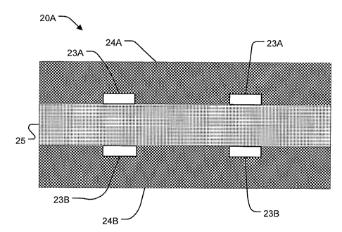
100191 Figures 2A and 2B show unit cell structures 20A and 20B according to
alternative embodiments of the invention. Structures 20A and 20B are similar
to one
another, and each comprise current-carrying structures 23A and 23B positioned
on
opposite sides of an ion exchange membrane 25. Electrochemical reaction layers
24A
and 2411 are positioned on the outside of current-carrying structures 23A and
23B and
-6-
CA 02564843 2006-10-27
WO 2005/106078
PCT/CA2005/000669
ion exchange membrane 25. The difference between structures 20A and 20B is
that in
structure 20A current-carrying structures 23A and 23B are positioned on the
outer
surfaces of ion exchange membrane 25, while in structure 20B current-carrying
structures 23A and 23B are embedded in the outer surfaces of ion exchange
membrane
25.
[00201 Figures 2C and 2D show unit cell structures 20C and 20D
according to
further alternative embodiments of the invention. In structure 20C, current-
carrying
structures 23A and 23B are formed on a substrate 30. Substrate 30 is
constructed from
a non-conducting material.
[0021] Substrate 30 is penetrated by an opening 32. Opening 32 is
filled with an
ion-conducting material. The ion-conducting material may comprise an ionomer
or
electrolyte suitable to the application. The ion-conducting material may
extend
outward to the outer edges of current-carrying structures 23A and 23B to form
ion
exchange membrane 25 of unit cell structure 20C. In the illustrated
embodiment,
opening 32 is round, but this is not necessary. Opening 32 may be of any
suitable
shape. In some embodiments, opening 32 is long and narrow. In some
embodiments,
each unit cell has a plurality of openings 32.
[0022] In some embodiments, openings 32 comprise a pattern of
openings,
which may be microstructured openings, as described, for example in the
commonly-
assigned application entitled "MICRO-STRUCTURED MEMBRANES AND
ELECTROCHEMICAL CELLS INCORPORATING SUCH MEMBRANES" which
is referred to above.
[00231 Examples of materials that may be suitable for substrate 30
in specific
applications include:
= printed circuit board (PCB) material,
-7-
CA 02564843 2006-10-27
WO 2005/106078
PCT/CA2005/000669
= polyamide films;
= polyimide films such as KaptonTM,
= polyethylene films,
= TeflonTM films,
= other polymer films,
= reinforced composite materials such as fibreglass,
= suitable non-polymer material such as silicon or glass.
In some applications it is advantageous that substrate 30 be flexible. In such
applications it is desirable that substrate 30 be made of a flexible material.
[0024] In structure 20D, current-carrying structures 23A and 23B
are formed on
proton conducting membrane 25 and there is no substrate 30. Structure 20D
differs
from structure 20A in that current-carrying structures 23A and 23B project
respectively through the outer surfaces of catalyst layers 24A and 24B. A
structure
like structure 20D may have its catalyst layers 24A and 24B divided into
isolated areas
by current-carrying structures 23A and 23B. Structure 20D has the disadvantage
that
the exposed surface area of catalyst areas 24A and 24B is somewhat reduced in
comparison to structures 20A, 20B, and 20C.
[0025] In each of unit cell structures 20A-D, current-carrying structures
23A
and 23B underlie portions of catalyst layers 24A and 24B respectively. In the
embodiments of Figures 2A-C, ions liberated at reaction sites which are over
current-
carrying structures 23A (or, in Figure 2C, over substrate 30) are blocked from
flowing
directly into and through ion exchange membrane 25 by the shortest straight-
line path.
Ions liberated at such sites must take longer paths to reach catalyst layer
24B.
However, by appropriately positioning current-carrying structures 23A and 23B,
the
thicknesses of the various layers and other dimensions (such as the width D of
opening
32 in Figure 2C) one can achieve a situation in which the lengths of paths
taken by
-8-
CA 02564843 2006-10-27
WO 2005/106078
PCT/CA2005/000669
ions and electrons are not very much longer than corresponding path lengths in
comparable prior art electrolytic cells.
[0026] The embodiment of Figure 2C trades off increased path
length for
proton conduction against the increased mechanical ruggedness resulting from
the
presence of substrate 30.
[0027] A feature of structures 20A through 20C is that the current-
carrying
structures 23A and 23B are not required to be porous because it is not
necessary for
reactants to pass through these structures.
[0028] Adjacent unit fuel cells may be connected in parallel by
either providing
current-carrying structures 23A and 23B that are common to the adjacent unit
cells, or
by electrically interconnecting current-carrying structures 23A of adjacent
cells and
current-carrying structures 23B of adjacent cells. Adjacent unit cells may
also be
electrically isolated from one another, in which case they may be connected in
series,
as discussed below with reference to Figures 6 and 6B. Electrical isolation of
unit cell
structures may be provided by rendering portions of a catalyst layer non-
conducting
electrically, by making a catalyst layer discontinuous in its portions between
unit cells
and/or by providing electrically insulating barriers between the unit cell
structures.
[0029] Optimising catalyst layer 24A to promote reactions does not
always
result in the highest electrical conductivity in catalyst layer 24A. The
materials used in
the catalyst layer may not be extremely good electrical conductors. However,
the
losses resulting from the electrical resistivity of catalyst layer 24A can be
minimized
by laying out each unit cell so that the distance between any point in
catalyst layer 24A
and the closest part of current-carrying member 23A is small.
-9-
CA 02564843 2006-10-27
WO 2005/106078
PCT/CA2005/000669
[0030] For example, in some embodiments of the invention the
longest path
length from any point within either catalyst layer 24A, 24B to the
corresponding
current-carrying member 23A, 23B is 5 mm. In other embodiments, the longest
path
length from any point within either catalyst layer 24A, 2413 to the
corresponding
current-carrying member 23A, 23B is 0.5 mm. Even smaller diameters are also
possible. In general, reducing the diameter decreases the ohmic losses
associated with
electrical current conduction in the catalyst layer. However, as the structure
becomes
smaller, the volume taken up current carrying members 23A, 23B increases in
proportion to the volume of the overall structure, and the space-efficiency of
the
structure can suffer.
[0031] Figure 3 illustrates a geometry that may be used for
approximating the
potential drop of an electrode 34 (which may be either an anode or a cathode).
Electrode 34 comprises a current-carrying structure 23A having a skin of ion
exchange
material 25A therein and catalyst layer 24A disposed outside thereof. Only the
portion
of catalyst layer 24A which is above current-carrying structure 23A is
depicted in
Figure 3. Electrode 34 is positioned opposite a corresponding electrode (not
shown in
Figure 3) on an outer surface of an ion exchange membrane (not shown in Figure
3)
which may or may not be a composite membrane having substrate 30 embedded
therein. In the Figure 3 embodiment, current-carrying structure 23A comprises
an
annular trace, wherein DT is the outer diameter of the circular trace, Ta and
TT are the
thicknesses of catalyst layer 24A and the circular trace, respectively, and WT
is the
width of the circular trace. In some embodiments, the ratio of trace diameter
to trace
width (D7-/WT) is at least 10.
[0032] Current-carrying structures 23A and 23B are constructed
from
electrically conductive materials. The following table lists some suitable
materials for
current-carrying structures 23A and 23B and their electrical conductivities:
-10-
CA 02564843 2006-10-27
WO 2005/106078
PCT/CA2005/000669
Material
Electrical Conductivity 107 (S/m)
Pure Copper 5.88
Pure Gold 4.55
Pure Nickel 1.43
Pure Platinum 0.96
Tin Oxide (Sn02; applied with a CO2 laser) 0.003125
[0033] Any electrically conductive materials may be used to
construct current-
carrying structures 23A and 23B. In some embodiments, current-carrying
structures
23A and 23B are constructed from metals that are either noble to begin with or
are
coated with a suitable material (Such as PEMCoatTm from INEOS ChlorTM Americas
Inc., Wilmington, Delaware) so that they resist corrosion. Corrosion can be a
problem
when metallic conductors are used in electrochemical cells, and fuel cells in
particular.
The cross sectional dimensions of current-carrying structures 23A and 23B can
be
chosen based on the total current desired to be carried and the electrical
losses which
are deemed acceptable in the design.
[0034] Current-carrying structures 23A and 23B may have
thicknesses, for
example, in the range of 5-75 m. In some embodiments, the thickness of
current-
carrying structures 23A and 23B is in the range of 25-50 p.m. Current-carrying
structures 23A and 23B need not have the same thickness. Where current-
carrying
structures 23A and 23B comprise annular traces, the traces may have a width of
5-200
m. In some embodiments, the traces may have a thickness on the order to 5 pm
and a
width on the order of 25 m. Current-carrying structures 23A and 23B can be
formed
using any suitable techniques. For example, various printed circuit board
fabrication
techniques may be used to form structures 23A and 23B. Laminating, P'VD,
sputtering
-11-
CA 02564843 2006-10-27
WO 2005/106078
PCT/CA2005/000669
and plating are examples of techniques that may be used alone or in
combination to
make the traces.
[0035] Catalyst layers 24A and 24B may be constructed from
materials which
conduct both electrons and the ions formed in the reactions which occur in the
cell in
which they are employed. (The ions are protons in hydrogen-fuelled PEM fuel
cells).
Catalyst layers 24A and 24B may comprise any type of electrocatalyst suitable
for the
application at hand. Catalyst layers 24A and 24B may comprise electrically-
conductive porous sintered powder materials, for example. For fuel cells the
catalyst
layers may comprise platinum on carbon, for example. In some embodiments,
catalyst
layers 24A and/or 24B comprise mixtures of carbon black and one or more of
PTFE
powder, PVDF powder, such as KynarTM powder, and silicon oxide powder. The
carbon black may comprise any suitable finely divided carbon material such as
one or
more of acetylene black carbon, carbon fibers, carbon needles, carbon
nanotubes,
carbon nanoparticles.
[0036] In some embodiments, catalyst layers 24A and 24B are formed
of
materials having electrical conductivities in the range of 50-200 S/m. Each
catalyst
layer 24A, 24B may be made up of several layers of different compositions.
[0037] In some embodiments, catalyst layers 24A and 24B have
thicknesses of
2501.tm or less. In some embodiments, the thickness of catalyst layers 24A and
24B is
about 10-25 lam. The thickness of catalys layers 24A and 24B may be about 20
psn,
for example. Catalyst layers 24A and 24B need not have the same thickness.
[0038] Where ion exchange membrane 25 has a composite structure
such as a
structure including a substrate 30, substrate 30 provides mechanical strength
to
membrane 25. The presence of substrate 30 permits membrane 25 to be made
thinner
than ordinary proton conducting membranes. This decreased thickness can
compensate
-12-
CA 02564843 2006-10-27
WO 2005/106078
PCT/CA2005/000669
to at least some degree for the more tortuous paths taken by protons which are
liberated at locations which are not immediately adjacent to apertures in
substrate 30.
In some embodiments, the thickness of membrane 25 is in the range of about 5
p.m to
about 250 p.m. The thickness of membrane 25 may be about 25 p.m, for example.
[0039] Figure 4 shows a portion of a unit cell structure 20E
according to
another embodiment of the invention. Unit cell structure 20E constitutes a PEM
fuel
cell with substrate 30 having a plurality of openings 32. A proton exchange
material
fills openings 32 and surrounds substrate 30 to form ion exchange membrane 25.
Figure 4 shows paths taken by protons (11) from three example reaction sites
33A,
33B and 33C in catalyst layer 24A of structure 20E, through ion exchange
membrane
25 and into catalyst layer 24B to three other example reaction sites 33D, 33E
and 33F.
Figure 4 also shows the paths taken by electrons (e) from reaction sites 33A,
33B and
33C to current-carrying structure 23A, and from current-carrying structure 23B
to
reaction sites 33D, 33E and 33F.
[0040] It can be seen that from reaction site 33A and 33B the
electron and
proton paths through catalyst layer 24A are roughly equal in length. From
reaction site
33A, which is over current-carrying structure 23A, the path taken by electrons
through
catalyst layer 24A is shorter than that taken by protons which must detour
around
current-carrying structure 23A. From reaction site 33C the path taken through
catalyst
layer 24A by protons is significantly shorter than that taken by electrons. In
the
illustrated examples, the paths taken by electrons and protons in catalyst
layer 24B to
reach reaction sites 33D, 33E and 33F have lengths similar to the lengths of
the paths
taken in catalyst layer 24A.
[0041] The paths taken by protons through ion exchange membrane 25
is not
equal, due to the presence of substrate 30. The protons must detour through
openings
32. In the examples illustrated, the path taken by the proton travelling from
reaction
-13-
CA 02564843 2006-10-27
WO 2005/106078
PCT/CA2005/000669
site 33B to reaction site 33E has the shortest distance through ion exchange
membrane
25, while the path taken by the proton travelling from reaction site 33C to
reaction site
33F has the longest distance through ion exchange membrane 25.
[00421 It can be seen in Figure 4 that the conductive species generated in
catalyst layer 24A (protons and electrons) both flow in generally the same
direction
(e.g. downward in Figure 4) to get from the reaction site where they are
liberated to
the conductor that will carry them. Likewise, the conductive species used in
the
reactions in catalyst layer 24B both flow in generally the same direction
(e.g.
downward in Figure 4) to get from the conductor to the reaction site.
[00431 Figure 5 shows an electrochemical cell layer 36 comprising
two unit cell
structures 20F. In the Figure 5 embodiment, cell layer 36 is formed from a
nonconducting sheet 26 which has been treated to form two ion-conducting
regions
27. Sheet 26 may, for example, be constructed of a copolymer of
tetrafluoroethylene
and perfluoro-3, 6-dioxa-4-methyl-7-octenesulfonyl fluoride (which is a resin
precursor to NafionTm), and may be selectively treated by a hydrolyzation
process to
form ion-conducting regions 27, as described, for example in the commonly-
assigned
application entitled "MICRO-STRUCTURED MEMBRANES AND
ELECTROCHEMICAL CELLS INCORPORATING SUCH MEMBRANES" which
is referred to above.
[00441 Current-carrying structures 23A and 23B are placed on
opposite sides of
sheet 26 around the periphery of each ion-conducting region 27. Current-
carrying
structures 23A and 23B may be ring-shaped, or may have different shapes. Ion-
conducting skins 25A and 25B may optionally be placed on the outer surfaces of
each
ion-conducting region 27 withip current-carrying structures 23A and 23B,
respectively. Ion-conducting skins 25A and 25B and ion-conducting region 27
together form ion-conducting membrane 25 for each structure 20F. Catalyst
layers
-14-
CA 02564843 2006-10-27
WO 2005/106078
PCT/CA2005/000669
24A and 24B are formed on the outer surfaces of current-carrying structures
23A and
2311 and ion-conducting skins 25A and 25B for each of cell structures 20F. In
the
illustrated embodiment, catalyst layers 24A and 24B for each cell structure
20F are
formed separately. However, a single catalyst layer 24A could cover one side
of both
structures 20F, and another single catalyst layer 24B could cover the other
side of both
structures 20F, if cell structures 20F are to be connected in parallel.
[0045] Neighboring unit cells may be electrically isolated from one
another. In
this case it is possible to electrically interconnect the unit cells in
arrangements other
than parallel arrangements. Vias may be used to interconnect adjacent unit
cells in
series. In embodiments in which unit cells are connected in series, catalyst
layers 24A
of the series connected cells are electrically isolated from one another.
Figure 6 shows
a cross section through a part of an electrochemical cell layer 40 in which a
number of
unit cells 42 are connected in series. Figure 6A illustrates schematically the
paths
taken by protons and electrons in the assembly of Figure 6.
[0046] In the embodiment of Figure 6, regions 44 are electrically
insulating.
Regions 44 may comprise a dielectric material, an air gap, or the like.
Regions 44
electrically isolate adjoining electrochemical unit cells from one another.
[0047] Current-carrying structure 23A of each unit cell 42 is
connected to the
current-carrying structure 23B of the adjacent unit cell 42 by an electrically
conductive
pathway 23C which passes through a via in substrate 30.
[0048] Figure 6B shows an electrochemical cell layer 40A wherein unit cells
are interconnected with one another by way of electrically conducting paths 46
embedded in substrate 30. Conducting paths 46 may be connected to current-
carrying
structures 23A and/or 23B by way of electrically conducting vias 47 formed in
substrate 30. The conducting paths may be used to interconnect unit cells in
series
-15-
CA 02564843 2006-10-27
WO 2005/106078
PCT/CA2005/000669
and/or in parallel with one another. A number of independent sets of
conducting paths
46 may be provided in or on substrate 30.
[0049] Electrochemical cell layer 40A of Figure 6B may be
constructed using a
multi-layer circuit board such as a flex circuit. This provides increased
current-
carrying capacity for the overall current collection system without reducing
the surface
area available for the cell reactions in the catalyst layers 24A and 24B.
[0050] Unit cells according to embodiments of the invention may
have any
suitable shapes and may be arrayed in any suitable manner. Figure 7 shows one
example of an electrochemical cell layer comprising a plurality of unit cell
structures
20D wherein the unit cells have a hexagonal configuration. The entire surface
of
structures 20D could be covered with a catalyst layer 24A if desired. In
alternative
embodiments the unit cells have elongated shapes in which a dimension along a
principle axis is significantly longer than a transverse dimension. For
example, such
unit cells may be shaped like elongated ellipses, elongated rectangles,
elongated
obround shapes or the like. The longer dimension of such unit cells may, for
example,
be at least 2, 5 or 10 times larger than the transverse shorter dimension.
[0051] It can be appreciated that various embodiments of the invention
described above (e.g., structures 20D and 40 or 40A) can be combined to
provide
assemblies of unit cells which are electrically interconnected in a series-
parallel
arrangement of any desired complexity. Generally available electrical
conductors
(such as suitable metals) have much less resistance to the flow of electrons
than do
generally available proton conductors to the flow of protons. Therefore, the
conductors
which carry electrons can have significantly smaller cross sectional areas
than do the
pathways which carry protons. Substrate 30 may comprise a multi-layer
structure (as,
for example, a multi-layer circuit board) in which case, conductors for
carrying
electrical currents may be embedded inside substrate 30.
-16-
CA 02564843 2006-10-27
WO 2005/106078
PCT/CA2005/000669
[00521 Figures 8A, 8B and 8C show various possible Ways in which
the unit
cells in a small array (in this example, a very small array having only 16
unit cells)
may be interconnected. In Figure 8A, unit cells 42 are connected in parallel.
The
output voltage is 1 (where 1 is the output voltage of a single unit cell) and
the output
current is N (in this case 16 times the maximum current of one unit cell). An
open
circuit failure of any one or more unit cells 42 will not prevent the array
from
operating (at a reduced output current) at the rated voltage (1 unit).
However, a short-
circuit failure of any one unit cell can prevent the entire array from
functioning.
[00531 In Figure 8B, unit cells 42 are arranged in a series
configuration. The
voltage output is N (in this case 16 times the voltage of a single unit cell).
The
maximum current output is 1. An open circuit failure of any one or more unit
cells will
prevent the array from operating. A short-circuit failure of any one or more
unit cells
will not prevent the array from providing current at a (reduced) maximum
output
voltage.
[00541 Figure 8C shows a number of unit cells 42 arranged in a
series-parallel
configuration. In this case, the array is interconnected so that there are
four groups of
unit cells connected in series. Each group of unit cells comprises four unit
cells
connected in parallel. Note that each unit cell is connected to a neighbor
which is
diagonally adjacent. Note that one of the groups of parallel connected unit
cells is split
into two parts which are located in spatially separated areas of the array. In
some
embodiments of the invention, unit cells of a group of unit cells are
spatially
distributed. This makes it less likely that a failure caused by trauma to an
area of the
array will cause all of the unit cells of a group to fail.
[00551 In the embodiment of Figure 8C the output voltage is 4 units
at a current
of four times the current capacity of one unit cell. The failure of any unit
cell in either
-17-
CA 02564843 2006-10-27
WO 2005/106078
PCT/CA2005/000669
a short-circuit mode or an open circuit mode will not prevent the array from
providing
current although the maximum available output voltage or current may be
reduced.
[0056] Large arrays of unit cells can be constructed to provide
large power-
generating electrochemical cell layers in which the entire electrochemical
structure is
contained within the layer. This means additional components such as plates
for
collecting currents etc. can be eliminated, or replaced with structures
serving different
functions. Structures like those described herein are well adapted to be
manufactured
by continuous processes. Such structures can be designed in a way which does
not
require the mechanical assembly of individual parts. Unlike 'edge collected'
cells, the
conductive path lengths within this structure may be kept extremely short so
that
ohmic losses in the catalyst layer are minimized.
[0057] An electrochemical cell layer comprising a plurality of
unit cells may be
constructed by providing a substrate comprising a plurality of ion conducting
regions.
Such a substrate could be provided, for example by selectively treating a
sheet of non-
or partially-conducting material to form the ion conducting regions, or by
selectively
treating a sheet of ion conducting material to form non-conducting regions, as
described, for example in the commonly-assigned application entitled
"MICRO-STRUCTURED MEMBRANES AND ELECTROCHEMICAL CELLS
INCORPORATING SUCH MEMBRANES" which is referred to above. Current-
carrying structures may be formed on each side of the substrate around the
periphery
of each ion conducting region by means of laminating, PVD, sputtering,
plating, or
other suitable techniques. An electrochemical reaction layer, which may
comprise a
catalyst, may be deposited on each side of the ion conducting regions, in at
least partial
contact with the current-carrying structures.
[0058] Individual unit cells may be very small. Other factors
being equal,
smaller unit cells can operate at improved efficiencies because the conduction
paths
-18-
CA 02564843 2011-11-04
for protons and electrons can be shorter in small unit cells than in larger
unit cells. The
unit cells can be very small, for example, 1 mm in diameter or smaller, or
even 500 um
in diameter or smaller. In some embodiments of the invention, unit cells have
active
areas of about e.g. 0.01 cm'. A typical air breathing fuel cell comprising a 1
mm
diameter unit cell may produce between about 1 and 3 mW of power. A fuel cell
layer
comprising 300-1000 such cells could produce 1 W of power.
[0059] An electrochemical cell according to this invention may have
as
few as 1 unit cell or may have a very large number, thousands or even
millions,
of unit cells formed on one substrate. Electrochemical cell structures made
according to some prototype embodiments of this invention have in excess of
500 unit cells, for example.
[0060] So far, substrate 30 and membrane electrode assemblies
generally have
been described as being planar. This is not necessary. Unit cells according to
the
invention may be used in an electrochemical cell layer that is pleated or
undulating as
shown, for example, in Figure 9. Such layers are very compact. Substantially
the entire
undulating area can be made active. Further, no porous layer is required
beyond the
catalyst layer and no unsupported face seals are required. Thus the undulating
area can
be tightly pleated since there is no porous medium between the pleats to
interfere with
the diffusion of fuel and oxidant to the exposed catalyst layers of the unit
cells. Unit
cells according to the invention may be incorporated in a pleated layer
structure as .
described, for example, in the commonly-assigned patent application entitled
"ELECTROCHEMICAL CELLS FORMED ON PLEATED SUBSTRATES" (US
7,201,986).
[0061] Figures 10 and 10A show a fuel cell device 50 according to
one
embodiment of the invention. Fuel cell device 50 comprises a fuel cell layer
52
comprising a plurality of unit cells 54. Fuel cell layer 52 comprises a
positive terminal
-19-
CA 02564843 2006-10-27
WO 2005/106078
PCT/CA2005/000669
53 and a negative terminal 55, which may be connected to an external circuit
(not
shown). Unit cells 54 may be connected between positive terminal 53 and
negative
terminal 55 in any suitable manner. Fuel cell layer 52 is sealed to a spacer
56, which
is in turn sealed to a base 58. Fuel cell layer 52, spacer 56 and base 58
define a
plenum 60 for holding fuel, which may be introduced through fuel inlet 62. An
optional fuel outlet 64 may be provided if fuel flow is required, or if
recirculation of
fuel is required. Base 58 could optionally be replaced with another fuel cell
layer,
oriented oppositely to layer 52. Also, spacer 56 could be built into layer 52,
such that
two such layers could be bonded back to back to form a fuel cell device having
two
fuel cell layers.
[0062] Figure 11 shows a non-planar fuel cell device 66 according
to another
embodiment of the invention. Device 66 is the same as device 50, except that
fuel cell
layer 68, spacer 70 and base 72 are curved. In the example illustrated in
Figure 11,
layer 68, spacer 70 and base 72 are shaped to conform to the wall of a
cylinder, but it
is to be understood that other non-planar configurations are equally possible.
[0063] Figure 12 shows a stack of fuel cell layers 52 and spacers
56 according
to another embodiment of the invention. Plenums defined by spacers 56 may be
filled
with fuel and oxidant in alternating fashion to provide reactants to layers
52.
[0064] Some embodiments of the invention provide unit cells wherein
an
exposed area of a catalyst layer is greater than a cross sectional area of an
ion-
conducting layer through which ions liberated by reactions in the catalyst
layer can
pass through the cell. This can be seen, for example, in Figure 2D wherein a
surface
124 of catalyst layer 24A has a surface area larger than a cross sectional
area of the
portion 125 of ion-conducting layer 25 through which ions (e.g. protons)
generated in
catalyst layer 24A pass to the opposing catalyst layer 24B.
-20-
CA 02564843 2006-10-27
WO 2005/106078
PCT/CA2005/000669
[0065] The invention also provides methods for operating
electrochemical cells.
One such method comprises:
= providing an electrochemical cell having: a catalyst-containing
electrochemical
reaction layer having an outer face and an inner face; an electrical current-
carrying structure underlying the electrochemical reaction layer at least in
part;
and an ion-conducting layer in contact with the inner face of the
electrochemical reaction layer;
= allowing a reactant to diffuse into the electrochemical reaction layer;
= allowing the reactant to undergo a catalysed electrochemical reaction to
produce an ion at a location in the electrochemical reaction layer between a
surface of the electrochemical layer and the current-carrying layer; and,
= allowing the ion to travel to the ion-conducting layer along a path that
avoids
the current-carrying structure.
The path taken by the ion is not substantially anti-parallel to a path taken
between the
by electrical current between the location and the current-carrying structure.
[0066] Where a component (e.g. a membrane, layer, device, circuit,
etc.) is
referred to above, unless otherwise indicated, reference to that component
(including a
reference to a "means") should be interpreted as including as equivalents of
that
component any component which performs the function of the described component
(i.e., that is functionally equivalent), including components which are not
structurally
equivalent to the disclosed structure which performs the function in the
illustrated
exemplary embodiments of the invention.
[0067] In some embodiments of the invention, a filter layer may be provided
on
the outer surface of one or both of catalyst layers 24A, 24B. The filter layer
may be
used to remove undesired materials from reactants before they reach catalyst
layer 24A
or 24B. For example, a filter layer placed over the cathode catalyst layer may
be
impermeable to water but permeable to air, to allow air to reach the cathode
of the unit
-21-
CA 02564843 2006-10-27
WO 2005/106078
PCT/CA2005/000669
cell, while preventing water from reaching the unit cell. Figure 13
illustrates an
example of structure 20A wherein a filter layer 200 is provided on the outer
surface of
catalyst layer 24B.
[0068] It is noteworthy that in a number of the embodiments described
above,
electrical current from electrochemical reactions occurring in a catalyst
layer is
collected in the plane of the catalyst layer.
[0069] As will be apparent to those skilled in the art in the
light of the foregoing
disclosure, many alterations and modifications are possible in the practice of
this
invention without departing from the spirit or scope thereof. For example:
= This invention has application to fuel cells as well as electrochemical
cells of
other types such as chlor-alkali reaction cells and electrolysis cells.
= The invention is not limited to gaseous fuels. Liquid fuels may also be
used
with appropriate material selections.
= The anodes and cathodes of the unit cells do not need to be the same
size. The
anodes may, for example, be somewhat smaller than the cathodes. Any exposed
traces could be located on the anode side of the membrane electrode
assemblies.
= The catalyst layers are layers where electrochemical reactions occur. In
some
embodiments these layers may not comprise catalysts in the strict sense of the
term.
= In some embodiments, the current-carrying structures are depicted as
being in
direct contact with the ion exchange membrane, but this is not necessary. It
is
to be understood that the current-carrying structures may be separated from
the
ion exchange membrane by another material, such as a portion of the catalyst
layer.
-22-
CA 02564843 2006-10-27
WO 2005/106078 PCT/CA2005/000669
[0070] Accordingly, the scope of the invention is to be construed in
accordance
with the substance defined by the following claims.
-23-