Note: Descriptions are shown in the official language in which they were submitted.
CA 02564995 2006-10-27
WO 2005/117152 PCT/US2005/016987
1
METHOD FOR FABRICATING GROUP III NITRIDE DEVICES AND
DEVICES FABRICATED USING METHOD
BACKGROUND OF THE INVENTION
Field of the Invention
This invention relates to a method for fabricating
a semiconductor device, and more particularly to method
for fabricating thin film semiconductor devices wherein
the growth substrate is renioved by a reactive ion etch.
Description of the Related Art
Improvements in the manufacturing of semiconductor
materials in the Group-III nitride material system has
focused interest on the development of GaN/AlGaN opto-
electronic devices such as high efficiency blue, green
and ultra-violet (UV) light emitting diodes (LED or LEDs)
and lasers, and electronic devices such as high power
microwave transistors. Some of the advantages of GaN is
its 3.4eV wide direct bandgap, high electron velocity
(2x10' cm/s), high breakdown field (2x10⁶ V/cm) and the
availability of heterostructures.
Typical LEDs can comprise an active region
sandwiched between a p-type doped layer, and an n-type
doped layer such that when a bias is applied across the
doped layer electrons and holes are injected into the
active region. The electrons and holes recombine in the
active region to generate light omnidirectionally in an
"emission sphere" with light radiating in all directions
within the material that makes up the LED structure.
CA 02564995 2006-10-27
WO 2005/117152 PCT/US2005/016987
2
Typical LEDs are efficient at generating light from the
active region, but the light has difficulties emitting
from the LED to the surroundings because of the
differences in the indexes of refraction between the LED
material and surroundings. In an LED having layers and
regions of a typical thickness, only the photons formed
in a cone about 20 wide in the direction of a surface
exit the structure. The remainder of the light is trapped
within the structure of the LED, and will eventually
become absorbed into the semiconductor material. The
light that is absorbed back into the LED material is lost
to light generation, which re'duces the overall emitting
efficiency of the LED.
Different methods have been developed for improving
the light emitting efficiency of typical LEDs, some of
which include using non-planar shaped LEDs and roughening
the emission surface of an LED. Both of these approaches
improve emitting efficiency by providing an LED surface
that has different angles such that when light from the
LED's active region reaches the surface with varying
angles between the light and the surface. This increases
the possibility that the light will be within the 20
cone when it reaches the surface such that it emits from
the LED. If it is not within the 20 angle, the light is
reflected at different angles, increasing the likelihood
that the light will be within the cone the next time it
reaches the surface.
Emission efficiency is also enhanced by utilizing a
resonant cavity structure in a resonant cavity LED
(RCLED). RCLEDs are generally described in E. Fred
Shubert, Light Emitting Diodes, Cambidge University
CA 02564995 2006-10-27
WO 2005/117152 PCT/US2005/016987
3
Press, Pages 198-211 (2003) . and typically comprise two
oppositely doped epitaxial layers and mirrors on the
oppositely doped layers such that the oppositely doped
layers are sandwiched between the mirrors. One of the
mirrors has reflectivity that is lower than the
reflectivity of the other mirror so that light exits the
RCLED through the lower reflectivity mirror. In other
embodiments, an epitaxial active region can be included
between the oppositely doped layers.
RCLEDs typically comprise epitaxial layers that are
much thinner than standard LEDs and a resonant cavity
effect appears when the thickness of the epitaxial layers
is approximately one wavelength of the light generated by
the epitaxial layers. The light generated in the resonant
cavity forms a standing wave such that all light emitted
is emitted directionally. This directional light emission
releases the photons in directions that are substantially
normal to a plane formed by the diode junction.
This structure allows RCLEDs to emit light intensity
along the axis of the cavity (i.e. normal to the
semiconductor surface) that is higher compared to
conventional LEDs. The. emission spectrum of RCLEDs has a
higher spectral purity compared to conventional LEDs and
the emission far-field pattern of RCLEDs is more directed
compared to standard LEDs.
I When fabricating RCLEDs of certail material systems
there are challenges in depositing the two mirrors on
opposite sides of epitaxial layers. The oppositely doped
layers (and active region) are typically formed on a
substrate using known fabrication methods and devices,
such as epitaxial growth in a metalorganic chemical vapor
CA 02564995 2006-10-27
WO 2005/117152 PCT/US2005/016987
4
deposition (MOCVD) reactor. Once these layers have been
deposited on the substrate the first of the two mirrors
may be deposited on the top, most recently grown
epitaxial surface, which is usually the p-type doped
layer. Placing a mirror surface on the surface of the
other doped, first grown layer is not so easy, because
the surface is in contact with the growth surface of the
substrate. The layers of RCLEDs are typically thin so it
can be difficult to separate the substrate from the
epitaxial layers so that the second mirror can be
deposited. It may not be practical to deposit the mirror
on the substrate and then grow the epitaxial layer
because of the crystal lattice mismatch between the
mirror material and epitaxial layers.
One of the ways to deposit the second mirror on the
epitaxial layers is to first remove the substrate. One
technique for removing the substrate from epitaxial
layers is described in U.S. Patent No. 6,071,795 to W.
Cheung et al. Thin films of GaN are epitaxially grown on
a sapphire substrate and the substrate is then laser
irradiated with a scanned beam at a wavelength at which
sapphire is transparent but the GaN is absorbing (e.g.
248mn wavelength)., The intensity of the radiation,
however, is low enough not to cause the irradiated area
to separate. The separation process is performed 'af ter
completion of the laser irradiation, such as by heating
the structure to above the melting point of gallium.
Another embodiment of the invention is described as
growing a sacrificial material between the desired film
and the growth substrate. The optical beam can then
CA 02564995 2006-10-27
WO 2005/117152 PCT/US2005/016987
irradiate from the side of either the growth or acceptor
substrate that is transparent to the optical beam.
The difficulty with this approach is that it is
particularly adapted to semiconductor devices grown on
5 sapphire substrates. Group-III nitride devices are often
grown on silicon carbide substrates and if the wavelength
of the irradiating optical beam is high enough not to be
absorbed by the silicon carbide, the wavelength can be
too high to be absorbed by the GaN. One alternative to
this is to find a wavelength of light that is transparent
to silicon carbide that will excite GaN. The difference
in bandgap between GaN and silicon carbide, however, is
too narrow to allow reliable transmission through the
silicon carbide while being absorbed by the GaN.
SUMMARY OF THE INVENTION
One embodiment of a method for fabricating high
light extraction photonic devices according to the
present invention comprises growing an epitaxial
semiconductor device structure on a substrate with the
epitaxial semiconductor structure and substrate
comprising an emitter adapted to emit light in response
to a bias. Flip-chip mounting the epitaxial semiconductor
structure and substrate on a submount such that the
epitaxial semiconductor device structure is sandwiched
between the submount and substrate. Etching the substrate
off the epitaxial semiconductor device~ by utilizing an
etch environment that etches the substrate is
substantially faster than the epitaxial semiconductor
structure.
CA 02564995 2006-10-27
WO 2005/117152 PCT/US2005/016987
6
A method for fabricating high light extraction
photonic devices according to the present invention
comprises growing an epitaxial semiconductor structure on
a substrate and depositing a first mirror layer on the
epitaxial semiconductor structure such that the epitaxial
semiconductor structure is sandwiched between the first
mirror layer and the substrate. The substrate is then
removed from the epitaxial structure by introducing an
etch environment to the substrate and a second mirror
layer is deposited on the epitaxial semiconductor
structure such that the epitaxial semiconductor structure
is sandwiched between the first and second mirror layers.
One embodiment of resonant cavity light emitting
diode (RCLED) according to the present invention
comprises a thin film epitaxial semiconductor structure
and a fist mirror layer on one surface of the eptaxial
semiconductor structure. A second mirror layer is
included on another surface of said epitaxial
semiconductor structure such that said epitaxial
semiconductor structure is sandwiched between the first
and second mirrors, the second mirror layer being less
reflective than the first mirror layer. A submount is
also included, said epitaxial semiconductor structure
with its first and second mirrors mounted on the
submount, the first mirror layer being adjacent to the
submount and the second mirror layer being the primiary
emitting surface.
A method for removing a silicon carbide substrate
from a Group-III nitride epitaxial semiconductor
material, comprising growing a Group-III nitride
epitaxial semiconductor material on a silicon carbide
CA 02564995 2006-10-27
WO 2005/117152 PCT/US2005/016987
7
substrate. An etch environment is introduced to the
silicon carbide substrate, the etch environment etching
silicon carbide faster than the Group-III nitride
epitaxial material such that the etching substantially
stops after the silicon carbide is etched off.
These and other features and advantages of the
invention will be apparent to those skilled in the art
from the following detailed description, taken together
with the accompanying drawings, in which:
BRIEF DESCRIPTION OF THE DRAWINGS
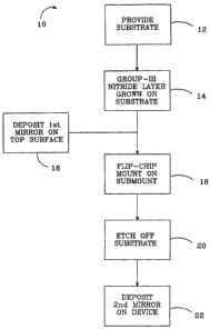
FIG. 1 is a flow diagram for one embodiment of a
fabrication method according to the present invention;
FIG. 2 is a sectional view of one embodiment of a
semiconductor device according to the present invention
at one of the intermediate steps of the method in FIG. 1;
FIG. 3 is a sectional view of another embodiment of
a semiconductor device according to the present invention
at one of, the intermediate steps of the method in FIG. 1;
FIG. 4 is a sectional view of = another embodiment of
a semiconductor device according to the present invention
at one of the intermediate steps of the method in FIG. 1;
FIG. 5 is a sectional view of another embodiment of
a semiconductor device according to the present invention
at one of the intermediate steps of the method in FIG. 1;
FIG. 6 is a sectional view of still another
embodiment of a semiconductor device according to the
present invention at one of the intermediate steps of the
method in FIG. 1;
FIG. 7 is a plan view of the semiconductor device in
FIG. 6;
CA 02564995 2006-10-27
WO 2005/117152 PCT/US2005/016987
8
FIG. 8 is a sectional view of one. embodiment of a
semiconductor device according to the present invention
at a flip chip step of the method in FIG. 1.
FIG. 9 is sectional view of the semiconductor device
in FIG. 8 after etching off the substrate according to
the method of FIG. 1;
FIG. 10 is. a sectional view of one embodiment of a
semiconductor device according to the present invention
at another intermediate step of the method in FIG. 1;
FIG. 11 is a sectional view of another embodiment of
a semiconductor device according to the present invention
at another step of the method in FIG. 1;
FIG. 12 is a sectional view of another embodiment of
a semiconductor device according to the present invention
at another step of the method in FIG. 1;
FIG. 13 is a sectional view of another embodiment of
a semiconductor device according to the present invention
at another step of the method in FIG. 1;
FIG. 14 is a sectional view of another embodiment of
a semiconductor device according to the present invention
at another step of the method in FIG. 1;
FIG. 15 is a sectional view of another embodiment of
a semiconductor device according to the present invention
at another step of the method in FIG. 1;
FIG. 16 is a plan view of the semiconductor device
in FIG. 15;
FIG. 17 is a sectional view of one embodiment of a
semiconductor device according to the present invention;
FIG. 18 is a sectional view of another embodiment of
a semiconductor device according to the present
invention;
CA 02564995 2006-10-27
WO 2005/117152 PCT/US2005/016987
9
FIG. 19 is a sectional view of another embodiment of
a semiconductor device according to the present
invention;
FIG. 20 is a sectional view of another embodiment of
a. semiconductor device according to the present
invention; and
FIG. 21 is a sectional view of still another
embodiment of a semiconductor device according to the
present invention.
DETAILED DESCRIPTION OF THE INVENTION
FIG. 1 shows one embodiment of a method 10 according
to the present invention for fabricating Group-III
nitride semiconductors, with the method , 10 being
particularly adapted for fabricating thin film Group-III
nitride semiconductor devices. In step 12, a substrate is
provided that can be made of many different materials,
with a preferred material being silicon carbide. SiC is a
suitable material for use with Group-III nitride
materials, such as GaN, because it has a closer crystal
lattice match to Group III nitrides GaN, which generally
results in Group III nitride films of high quality.
Silicon carbide also has high thermal conductivity so
that the total output power of Group III nitride devices
on silicon carbide is not limited by the thermal
dissipation of the substrate (as is the case with some
devices formed on sapphire). SiC substrates are available
from Cree Research, Inc., of Durham, North Carolina and
methods for producing them are set forth in the
scientific literature as well as in a U.S. Patents, Nos.
Re. 34,861; 4,946,547; and 5,200,022.
CA 02564995 2006-10-27
WO 2005/117152 PCT/US2005/016987
In step 14 Group-III nitride epitaxial layer(s) are
grown on the substrate using any of the known
semiconductor fabrication processes such as molecular
beam epitaxy (MBE) or metal organic chemical vapor
5 deposition (MOCVD). Depending on the type of device being
fabricated, an optional step 16 .is included that
comprises depositing a first mirror layer on the surface
of the epitaxial layers opposite the substrate. As will
be understood by the discussion below, if a light
,10 emitting diode (LED) is being fabricated, this mirror
helps increase the useful light extraction of the LED,
and if an RCLED is being fabricated this mirror is
necessary to generate the resonant cavity effect.
Different mirrors can be used, such as metal mirrors made
of materials such as silver, gold, rhodium, platinum,
palladium, gold tin or combinations thereof, which can be
deposited on the surface using-a conventional method such
as sputtering. Alternatively, the mirror can be a
distributed Bragg reflector (DBR) which generally
comprises multiple pairs of two materials having
different refractive indexes. As a result of the
difference in the refractive index, Fresnel reflection
occurs at each of the interfaces. The reflection at each
may not be total, but because of the number of interfaces
and the thicknesses of the different layers, the
reflected waves constructively interfere so that the DBR
provides good reflectivity. Depending on the type of
material used for the DBR, it can be deposited on the top
surface using the same method used to fabricate the
epitaxial layer, usually MBE or MOCVD.
CA 02564995 2006-10-27
WO 2005/117152 PCT/US2005/016987
11
Tn step 18, the substrate, with its epitaxial layers
and first mirror layer, is flip-chip mounted to a
submount such that the top surface of the epitaxial
layers, or the mirror, as the case may be, is adjacent to
the submount. The surface of the eptitaxial layer or
mirror layer can be bonded to the substrate using many
known materials, one example being silver tin eutectic.
The submount can be one of a single construction or can
include a number of different structural members, and can
be made of different materials such as silicon, silicon
carbide, sapphire, glass or metals. The submount can also
include electronic components to drive the device that
comprises the Group-III epitaxial layers.
In step 20, the substrate is etched off of the
eptixial layers with the preferred etch being a
composition that selectively removes the substrate at a
high etch rate while etching the eptitaxial layers at a
very low etch rate. In one embodiment according to the
present invention, the etch material can be nitrogen tri
fluoride, which etches silicon carbide at a rate many
times faster than in etches Group-III nitride epitaxial
layers. Ions of nitrogen tri fluoride readily remove
silicon carbide down to its interface with the Group-III
nitride materials. Once the silicon carbide is removed,
etching essentially stops because the etch rate of the
epitaxial layers is so slow.
Depending on the device being fabricated alternate
step 22 can be included wherein a mirror can be deposited
on the surface of the epitaxial layers that is revealed
by the etching process. This step is usually included
when fabricating a resonant cavity LED (RCLED), solid
CA 02564995 2006-10-27
WO 2005/117152 PCT/US2005/016987
12
state laser, or vertical-cavity surface-emitting laser
(VCSEL).
The method 10 can be used in fabricating many
different semiconductor devices having epitaxial layers
made of many different materials with many different
thicknesses. The method 10 is particularly adapted to
growing high quality thin film Group-III nitride layers
used in RCLEDs, which mirrors on the opposing sides of
the thin films. When forming a Group-III nitride RCLED it
is impractical to provide a mirror on the interface
between the SiC substrate epitaxial layer because mirrors
either have no recognizable monocrystalline structure or
they are monocrystalline with a significantly different
sized crystal lattice than that formed by epitaxial
layers. As a result, it is difficult to fabricate high
quality thin Group-III nitride layers on a mirror surface
because of the mismatch in crystal structures.
SiC substrates, on the other hand, have a good
crystal lattice match to Group III nitrides which
generally results in thin Group III nitride layers of
high quality. The thin epitaxial layers can require
support during processing steps that follow growth on the
substrate, and the method 10 allows for the first mirror
to be deposited on the one surface of the epitaxial
layers while the substrate is in place and supports the
thin layers. The device is then flip chipped on a
submount with the first mirror between the submount and
layers. The submount provides additional support while
the substrate is etched off and the second mirror is
deposited. By providing this support through processing,
CA 02564995 2006-10-27
WO 2005/117152 PCT/US2005/016987
13
high quality thin film devices can be fabricated in the
Group-III nitride material system.
FIG. 2 shows one embodiment of a RCLED 30 according
to the present invention that is fabricated using the
method 10, with the RCLED 30 shown at one of the
intermediate steps in the method 10. The RCLED 30
comprises a silicon carbide substrate 32 that is used to
anchor the epitaxial growth and has a first substrate
surface 34 upon which the epitaxial growth nucleates. The
first substrate surface 34 then becomes the interface
between silicon carbide substrate 32 and epitaxial device
structure 36. In this embodiment epitaxial structure 36
comprises an n-type GaN layer 38 that is grown directly
on silicon carbide substrate 32 and a p-type GaN layer 40
that is grown on top of n-type layer 38. In other
embodiments, an active region can be included between the
n-type and p-type layers. The RCLED 30 further comprises
a first mirror 42 that is deposited on the exposed
surface of p-type epitaxial layer 32. The RCLED 10 is
shown as it 'could appear after step 16 in method 10 of
FIG. 1.
FIGS. 3-7 show different embodiments of a RCLED
according to the present invention as it could appear
after step 16 in method 10, with different mirror
structures. FIG. 3 shows an RCLED 50, which has many of
the same layers and the RCLED 30. For those layers that
are the same in this figure (and the figures that follow)
the same reference numerals will be used and the features
will not be reintroduced. In RCLED 50 the first mirror 52
comprises a p-type metal mirror that can be made of
CA 02564995 2006-10-27
WO 2005/117152 PCT/US2005/016987
14
silver, gold, rhodium, platinum, palladium or gold tin or
combinations thereof.
FIG. 4 shows another embodiment of a RCLED 60 also
having many of the same layers as RCLED 30, but wherein
the first mirror 62 is a DBR as described above in method
10. DBR first mirror 62 can be made of many different
layer pairs having different thicknesses and different
indexes of refraction, with the DBR first mirror 62
preferrably made of alternating dielectric layers of
quarter wavelength thicknesses p-type silicon dioxide 64
and p-type titanium oxide 66. Another embodiment of the
DBR first mirror 62 according to the present invention
comprises alternating dielectric layers of silicon
dioxide and tantalum pentoxide. The contrast in
indexes of refraction between device structure 36 made of
GaN and layers 64, 66 that form DBR first mirror 62 is
sufficient that the DBR first mirror 42 effectively
reflects light with two to four alternating layer pairs,
with a suitable number of alternating layer pairs being
three, although a DBR first mirror 62 with fewer or more
pairs can also be used. The thickness of these layers
corresponds to a quarter wavelength of light generated by
the epitaxial device structure 36 when a bias is applied
across the n-type and p-type layers 38, 40.
FIG. 5 shows another embodiment of an RCLED 70
having a f irst mirror 72 that is also a DBR made of p-
type alternating pairs, with the alternating pairs made
of an epitaxial material. Many different alternating
pairs can be used, with the DBR first mirror 72
comprising alternating pairs of p-type GaN 74 and p-type
aluminum nitride 76. In other embodiments of the DBR
CA 02564995 2006-10-27
WO 2005/117152 PCT/US2005/016987
first mirror 72 aluminum alloy nitride can be used
instead of aluminum nitride. The index of refraction
difference between epitaxial device structure 36 and the
material that comprises DBR first mirror 72 is such that
5 the mirror 72 requires approximately eight to twelve
layer pairs that are approximately a quarter wavelength
thick, with a suitable number of layer pairs being ten.
It is understood that the DBR will also work with fewer
and more layer pairs.
10 One concern when fabricating Group-III nitride LEDs
is ensuring that current spreads from the contacts
throughout the n-type and p-type layers such that the LED
uniformly emits light. N-type Group-III nitride material
is a good conductor, so current typically spreads from
15 its contact - throughout the layer. P-type Group-III
nitride material, conversely, is not a good conductor and
current has difficulty spreading from a contact,
particularly for larger devices. The metal mirror 52 in
FIG. 3 is a good conductor and will spread current from a
contact throughout the p-type layer. The p-type DBR
mirrors 62, 72 described above in FIGs. 4 and 5, however,
do not effectively conduct electricity and have
difficulty spreading current from a contact throughout
the p-type layer.
FIG. 6.shows a RCLED 80 that combines the DBR p-type
first mirror 82 with a metal mirror to enhance current
spreading into the p-type layer 40, with the first mirror
82 comprising a DBR 84 with a metal mesh 86 to spread
current from a contact. The DBR 84 is deposited= on
epitaxial structure 36 with a sufficient number of layers
of appropriate thickness to be highly reflective.
CA 02564995 2006-10-27
WO 2005/117152 PCT/US2005/016987
16
Channels are then opened in DBR 84, usually by etching,
which extend across the surface of the p-type layer 40
and are interconnected. These channels are then filled
with metal mirror material to form the metal mesh 86. DBR
84 has a higher reflectivity of metal 86, but the
combination of metal 86 and DBR 84 comprises a layer with
sufficient reflectivity and good current spreading. FIG.
7 is a top plan view of RCLED 80 showing the top surface
of the DBR 84 and metal mesh 86. The metal mesh is shown
as orthogonal and interconnected channels, although the
mesh can have many different channel arrangements.
FIG. 8 shows an RCLED 90 after it is flip chip
mounted on a submount pursuant to'step 18 in the method
10 of FIG. 1. The RCLED has many of the same features of
RCLED 30 in FIG. 2 and, as with the FIGs. 3-7, the same
reference numerals are used for the same features. The
RCLED 90 can be any one of the RCLEDs described above in
relation to FIGs. 2-7 and is flipped and adhered to a
submount 92 by a bonding layer/material 94 with the
mirror layer 96 adjacent to the submount 92. In one
embodiment according to the invention the bonding
layer/material 94 comprises a submount epoxy material
comprising silver tin eutectic. As described above,
submount 92 can be one of many structural members
including silicon, silicon carbide, sapphire, glass or
metals.
Once the RCLED 90 is bonded to submount 92 the
substrate 32 can be removed from the structure 36,
preferably by etching. The RCLED 90 with its submount 92
(hereinafter referred to as "RCLED 90") can be placed in
a reactive ion etch chamber having a reactive ion etch
CA 02564995 2006-10-27
WO 2005/117152 PCT/US2005/016987
17
environment 98 that etches the substrate 32 at a high
rate and etches the epitaxial layers at a slow rate'. One
embodiment of an etch environment according to the
present invention comprises ions of nitrogen tri-
fluoride, with the ions readily reducing and removing
silicon carbide substrate 12 from the RCLED 30 until the
surface of the epitaxial device structure 36 is reached,
in this case the surface of the n-type epitaxial layer.
Because the etch rate for silicon carbide is
significantly greater than the etch rate of GaN, once all
of silicon carbide substrate 12 has been removed, etching
essentially ceases.
FIG. 9 shows the RCLED 90 of FIG. 8 with the
substrate removed by the reactive ion etch after step 20
in the method 10 of FIG. 1. The reactive ion etch in one
embodiment can leave the top surface of semiconductor 30
in a condition ready to receive epitaxial growth or
deposition of a metal for a second mirror.
FIG. 10-15 show different embodiments of an RCLED
according to the present invention after step 22 of the
method 10 in FIG. 1, with the different RCLEDs comprising
different types of second mirrors. FIG. 10 shows one
embodiment on the RCDLED 90 of FIG. 9 with a second
mirror layer 100 on the newly exposed surface of the n-
type layer 38. The second mirror layer 100 can be many
different mirror types such as an n-type metal mirror, an
n-type DBR or an n-type epitaxial Bragg reflector. The
second mirror layer 100, however, should have a lower
reflectivity than the first mirror so that light exits
the RCLED through the second mirror layer 100. As shown
in FIG. 11, the first mirror layer 96 can also be any of
CA 02564995 2006-10-27
WO 2005/117152 PCT/US2005/016987
18
a metal layer, a p-type Bragg reflector DBR, or a p-type
epitaxial mirror. Metallization layer 102 cab be
deposited on the exposed surfaceof second mirror n-type
layer 100 and can be any of gold, silver, rhodium,
palladium, platinum or gold tin for bonding.
FIGS. 12-15 show embodiments of a RCLED according to
the present invention, each of which uses a different
type of second mirror layer. FIG. 12 shows a RCLED 110
according to the present invention utilizing an n-type
metal for its second mirror layer 112 that can be made of
the same material as mirror layer 52 described above and
shown in FIG. 3. FIG. 13 shows a RCLED 120 according to
the present invention utilizing an n-type DBR as its
second mirror layer 122. The DBR mirror layer is similar
to the p-type DBR first mirror 62 shown in FIG. 4 and can
be made of many different alternating pairs, but is
preferably made of approximately three alternating pairs
of a silicon dioxide layer 124 and a titanium dioxide
126. FIG. 14 shows a RCLED 130 according to the present
invention also utilizing a DBR as its second mirror layer
132 that is similar to the DBR first mirror layer 72 in
FIG. 5 and comprises approximately ten pairs of n-type
GaN 134 and n-type aluminum nitride 136.
Although current spreading is not so much of a
concern for n-type Group-III nitride materials, current
spreading structure can also be included in the second
mirror layer. FIGs. 15 and 16 show an embodiment of an
RCLED 140 according to the present invention wherein the
second mirror layer 142 comprises an n-type DBR 144 with
a metal mesh that is similar to the DBR 84 and metal mesh
86 described above and shown in FIGs. 6 and 7, with the
CA 02564995 2006-10-27
WO 2005/117152 PCT/US2005/016987
19
metal mesh 86 providing for good current spreading
throughout the n-type epitaxial layer 38.
FIGS. 17-20 show different embodiments of an RCLED
according to the present invention that can be fabricated
using the method 10 in FIG. 1. In each of the RCLEDs
shown, the first mirror layer can be any of the metal
mirror deposition, the p-type DBR, or the p-type
epitaxial DBR. Similarly, in each of the RCLEDs that
second mirror layer can be an n-type metal mirror, n-type
DBR, or n-type epitaxial DBR. In these figures the
selection of the second mirror layer is not constrained
by the selection of the first mirror layer and vice
versa. For example, second mirror layer can be an n-type
metal mirror when first mirror layer is a p-type DBR.
FIG. 17 shows one embodiment of an RCLED 150
according to the present invention that can be fabricated
using the method 10 in FIG. 1. As described above, RCLEDs
require 'that the epitaxial structure 36 be thin, having a
thickness of approximately one wavelength of the light
being emitted by the structure 36. The method 10 provides
for the fabrication of high quality Group-III nitride
thin layers particularly adapted to RCLEDs. The first and
second mirror layers 152, 154 can be any of those
described above and the RCLED 150 also comprises a
contact metal layer 156 on the second mirror layer 154.
The p-type layer 40 can be contacted through the submount
92 such that the RCLED 150 emits light in response to a
bias applied across the submount 92 and the contact metal
layer 156.
The method 10 in FIG. 1 can also be used in the
fabrication of devices having epitaxial layers that are
CA 02564995 2006-10-27
WO 2005/117152 PCT/US2005/016987
thicker than those ' in RCLEDs. FIG. 18 shows one
embodiment of a standard LED 160 according to the present
invention, fabricated by the method 10. The epitaxial
structure 162 has dimensions significantly larger than
5 those of epitaxial structure 36 in the RCLEDs above, but
the method 10 is equally adapted to the fabrication of
devices with thicker layers. The LED 160 also has an n-
type contact 164 to provide a current to one of the
oppositely doped layers in the structure 162, with the
10 other of the oppositely doped layers contacted through
the submount 166.
The method 10 can also be used in fabricating
epitaxial devices that have other features to enhance
light extraction. FIG. 19 shows an embodiment of LED 170
15 that has shaped side surfaces 172, 174 and is roughened
on its primary emitting surface 176. The LED 170 is
typically shaped and roughened after the substrate
removal method 10 is complete. Shaping and roughening the
LED 170 increases the light extraction of the LED 170 by
20 increasing the fraction of light that hits the surface
and escapes to emit light from the device.
All of the devices described herein can also be
fabricated with additional layers and features, one of
them being a structure to protect the device from eletro-
static discharge (ESD) . FIG. 20 shows an LED 180 that is
similar to the LED 170 of FIG. 19, but includes a zener
diode 182 arranged between the submount 184 and the first
mirror layer 186. The zener diode 182 is integrated into
the submount 184 during submount fabrication and
constrains the flow of current through the LED to one
direction only. The LED shown also has angled side
CA 02564995 2006-10-27
WO 2005/117152 PCT/US2005/016987
21
surfaces 186, 187 and a roughened emitting surface 188.
When fabricating LED 180 using the method 10, the
submount 184 is provided with the zener diode structure
182, such that when the device is flip-chip mounted on
the submount 184 the zener diode structure 182 is
integral with the device. The resulting structure
provides high light extraction efficiency and high ESD
rating. It is understood that the zener diode structure
can be included in many different devices according to
the present invention, including the different
embodiments of the RCLEDs described above as well as
vertical cavity surface emitting lasers and laser diodes.
The method 10 can also be used to fabricate other
devises such as a vertical cavity surface emitting laser
(VCSEL). FIG. 21 shows one embodiment of a VCSEL 190
according to the present invention fabricated by the
method 10. In this embodiment the first and second
mirror layers surfaces 192, 194 are DBR mirrors. First
DBR mirror 192 is shown adhered to submount 92 by an
epoxy epoxy/metallization 94. The quantum well structure
of this embodiment is a single quantum well having a
lower cladding layer 196 that can be fabricated from
aluminum indium gallium nitride. Quantum well 198 is
arranged above lower cladding layer 196, and the quantum
well 198 can be fabricated in one example from indium
gallium nitride. Upper cladding layer 200 is arranged
above the quantum well 198, such that the quantum well is
sandwiched between the upper and lower cladding layers
200, 196. Upper cladding layer 200 can be fabricated from
aluminum gallium nitride.
CA 02564995 2006-10-27
WO 2005/117152 PCT/US2005/016987
22
The second DBR mirror layer 194 is deposited on top
of upper cladding layer 200. This structure may be etched
away to form isolated columns that can be round or
rectangular. These isolated columns may then be further
isolated by isolation epitaxial growth 202. In one
embodiment the isolation material may be ion implanted.
Implantation may damage the crystalline structure between
the cells which would require annealing. The device is
capped off with metallization 204. Metallization uses
isolation structures for support but since the isolation
structure does not conduct electricity the metallizations
must at least partially contact mirror 194.
Although the present invention has been described in
considerable detail with reference to certain preferred
configurations thereof, other versions are possible. The
methods according to the present invention can be used to
fabricate many different devices and the devices
described above can have many different layer
arrangements. Therefore, the spirit and scope of the
appended claims should not be limited to the preferred
versions in the specification.