Note: Descriptions are shown in the official language in which they were submitted.
CA 02565279 2006-10-23
Electric Connection Terminal for a Printed Circuit Board
Field of the Invention
The invention pertains to an electric connection terminal for a printed
circuit
board that composed of a connector part, the insulating housing of which
features several sockets in which electric contacts with a mating side and a
terminal side are arranged.
Background of the Invention
A connection terminal of this type is required for achieving greater creepage
distances and clearances for spark over voltages in electric contacts that are
arranged relatively close to one another in a connector housing and also
acted upon with higher voltage values. In this case, a higher electric
strength
is also ensured in the direct mating region on the printed circuit board.
Description of the related art
EP 1 289 075 discloses a plug connector with an insulating and sealing ele-
ment of an elastic insulating material with high electric strength that is ar-
ranged on the bottom of a plug connector housing and provided with
through-openings for the electric contacts.
CA 02565279 2006-10-23
2
Summary of the Invention
Consequently, the invention is based on the objective of designing a connec-
tion terminal for producing a plug-type connection on a printed circuit board
in such a way that the safety clearance realized for the continuing strip con-
ductors connected to the electric contacts of the connector part suffices for
preventing sparkover voltages between the strip conductors when higher
voltages are transmitted to the printed circuit board.
This objective is attained in that the terminal sides of the electric contacts
protrude at least partially into separate chambers of a snap-on element that
can be positioned over the sockets of the connector part from the terminal
side.
Advantageous embodiments of the invention are disclosed in Claims
2-4.
The inventive connection terminal consisting of a connector part and a snap-
on element is rigidly connected to a printed circuit board and designed for
producing a direct electric connection for relatively high voltages of approxi-
mately 450 V per electric contact with a mating connector.
The advantages attained with the invention can be seen, in particular, in that
the snap-on element provided with separate chambers at least regionally
encloses the electric contacts arranged in an insulating member of the con-
nector part, and in that a separation of the soldering points connecting the
electric contacts with the electric strip conductors on the printed circuit
board
is simultaneously ensured.
The connector part is manufactured from an electrically insulating material
and features a square support plate with several sockets inserted or inte-
grated therein, wherein the electric contacts are inserted into these sockets
CA 02565279 2006-10-23
3
such that they protrude from the sockets in the form of connector pins on
one side and in the form of terminal pins on the other side.
The connector part is placed on the component side of the printed circuit
board with the side featuring the terminal pins such that the electric
contacts
are inserted into the bores and can be subsequently soldered to the solder-
ing points on the rear side (solder side).
The snap-on element with the chamber walls forming the chambers is then
inserted into the slots provided in the printed circuit board for this purpose
from the solder side such that the chamber walls enclose a region of the
electric contacts above and underneath the support plate and, in particular,
separate the individual soldering points, wherein the regions that
respectively
point outward remain open.
In addition, it is possible to provide an interlocking connection between the
connector part and the snap-on element such that forces--tensile or shearing
forces--acting upon the connector part and the electric contacts are transmit-
ted to the printed circuit board via the interlocking connection so as to
allevi-
ate the load on the soldering points on the printed circuit board.
Brief Description of the Drawings
One embodiment of the invention is illustrated in the figures and described in
greater detail below. The figures show:
Figure 1, a perspective representation of a connector part;
Figure 2, a perspective representation of a snap-on element;
Figure 3, an illustration of a printed circuit board that features slots and
soldering points;
CA 02565279 2006-10-23
4
Figure 4, a connector part with a snap-on element that is mounted on
the printed circuit board;
Figure 5, another illustration of the connector part with the snap-on
element, and
Figure 6, a detailed representation of a mounted snap-on element with
the connector part.
Detailed Description of the Invention
Figure 1 shows an isometric representation of a connector part 1 of an elec-
tric connection terminal to be mounted on a printed circuit board 20.
The connector part comprises a support plate 5 that is manufactured from an
insulating material and contains sockets 6 for accommodating electric con-
tacts 8 with a mating side 3 and a terminal side 4 that is realized in the
form
of the solder side in this case.
The support plate 5 is arranged centrally referred to the length of the
sockets
6 and extends approximately perpendicular thereto.
Spacers 7 moulded onto the respective outer sockets 6 ensure that a mini-
mum distance between the sockets and the printed circuit board is main-
tained.
Figure 2 shows an embodiment of a snap-on element 10 with an isosceles,
cruciform base plate 11 and vertically aligned chamber walls 12 moulded
thereon.
In this case, a total of four chambers 13 are formed, wherein three chambers
have a square shape and one chamber has a rectangular shape, and
wherein the rectangular chamber has a size that corresponds to that of two
square chambers.
CA 02565279 2006-10-23
One peculiarity of the chambers is that the respective sides that point out-
ward are open rather than closed with a wall.
Likewise, the outwardly positioned corner regions are open on two sides.
5
Hooks 16 are moulded onto the respective outer sides of the horizontally ar-
ranged chamber walls and can be engaged with the snap-on element 10 af-
ter it is inserted into the printed circuit board 20, wherein the webs 15 at-
tached to the hooks 16 are provided for ensuring a secure seat of the snap-
on element.
Figure 3 shows a detail of a printed circuit board 20 with several bores 21
arranged therein, wherein rectangularly aligned slots 23 are arranged be-
tween the bores.
This figure shows eight bores 21 with soldering points 22 that serve as con-
necting points for being soldered to the terminal side 4 of the electric con-
tacts of the connector part.
The regular strip conductors connected to the soldering points 22 are not
illustrated in the figure.
However, one can ascertain that each soldering or connecting point 22 is
respectively separated from the adjacent soldering or connecting point by the
slots 23.
Figure 4 shows an isometric representation, in which the predominant view-
ing direction is directed at the solder side of the printed circuit board 20,
the
snap-on element 10 inserted into the slots 23, as well as the connector part
with the housing that is inserted into the bores 21 of the soldering points
22,
wherein the solder or terminal side 4 of the electric contacts 8 already pro-
trudes from the bores 21 on the solder side of the printed circuit board. One
can ascertain that the end faces of the cross respectively feature an open
CA 02565279 2006-10-23
6
side 14, wherein all soldering points 22 and the contacts 8 are separated
from one another in an electrically insulated fashion as well as optically.
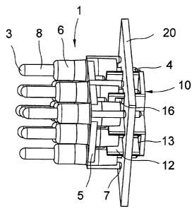
Figure 5 shows a side view of the connector part 1 arranged above the
printed circuit board 20 (in this case on the left side) and the snap-on ele-
ment 10 that is inserted into these slots 23 with the chamber walls 12 under-
neath the printed circuit board (in this case on the right side).
The spacers 7 are moulded onto the outer regions of the corner sockets 6,
to wherein these spacers begin at the support plate 5 and ensure that a mini-
mum distance between the sockets 6 and the printed circuit board 20 is
maintained.
Figure 6 shows a significantly enlarged detail of Figure 5.
This figure shows the sockets 6 that are respectively arranged separately in
the individual chambers 13 of the snap-on element 10, as well as the termi-
nal sides 4 of the electric contacts arranged in these sockets.
The chamber walls 12 are inserted into the slots 23, wherein this figure also
shows one of the hooks 16 that engages with the snap-on element 10 on the
component side of the printed circuit board 20 when it is pushed through the
slots 23.