Note: Descriptions are shown in the official language in which they were submitted.
CA 02565444 2009-04-27
WO 20M I2184 PCT{f152OttSl022197
TrI1 OF THfl INVENTION
COATED ARTICLE HAVING LOW -E COATING WMTH ION BEAM
TREATED 1R REFLECflNG LAYER AND CORRESPONDING METHOD
(0001] This invention relates to a coated article inchlding a solar control
coating s uch as a low-emlaaivity (low-B) In" r'' n mcampic embodiments.
the low B exerting includes an infrared (IR) reflecting layer(s) of a material
such as
silver (Ag) or the like which is ion beam treated. In certain example
embodiments,
the ion beam treat nent is pexlbmsed in a mannet so as to canes the 1R
reflecting layer
to realize compressive stress (as opposed to unreal tensile stria) And/or to
reduce
electrical resistance (sheet resistance R. and/cc bulk resisWice) of the
coated article.
Coaxed articles according to certain example embodiments of this invention
[nary be
used in sire contact of vehicle windshields. insulating glass (IG) window
emits, other
typos of windows, or in any other suitable application.
BACSGROUND OP THE INVENTION
[0002] Coated articles are known in the art for use in window applications
sues as nawaung glass (iii) wlndiaw oaths, velilcle windows. and/or t) 1e
liite.
Example non-linsiting low-emissivity (1rnwB) coatings am r"llmtteted sndlar
deidbed
in U.S. Patent tlocnme nt Noa. 6.723.211; 6,576,349; 6,447,891; 6,461,731;
3,682,528: 5,514,476; 5,425,861; and 200310150711,
(0003] In certain situations, designers of coated articles with low-B coatings
often strive for a combination of bill visible transmission, substantially
neutral color,
low emissivity (or emittauce), low shed re ce W. and good durability. Egh
visible transmission for example may pmmlt coated articles to be mere
desirable in
applications such as vehicle windshields or the like, whereas low-emissivity
pow E)
and low sheet resistance (R.) cftacacmaativs permit such coated eticlea to
block
sigsillleant amounts of IR r adution so as to educe for example and sirable
heating of
vehicle or building interiors. It is often dif$cult to obtain high visible
transmission
and adequate solar oonttol gropesttes ssmeh as gaol Ili blockage, combined
with good
1
CA 02565444 2006-11-01
Printed: 1 8/05/2006: DESCPAMD US0522197
durability (chemical and/or mechanical durability) because materials used to
improve
durability often cause undesirable drops in visible transmission and/or
undesirable
color shifts of the product upon heat treatment.
[0004] Low-E coatings typically include one or more IR reflecting layers. An
IR reflecting layer is typically metallic or mostly metallic, and is often of
a material
such as silver (Ag), gold (Au), or the like. The silver or gold may be doped
with other
materials in certain instances. The purpose of the IP, reflecting layer(s) is
to block
significant amounts of IR radiation, thereby preventing the same from
undesirably
heating up vehicle and/or building interiors which the coated article is
protecting.
[0005] Generally speaking, the lower the electrical resistance (sheet
resistance
RS and for bulk resistance) of an IR reflecting layer, the better the IR
reflecting
characteristics thereof. However, it has heretofore been difficult to reduce
resistance
properties (and thus improve IR reflecting characteristics) of an IR
reflecting layer
without adversely affecting optical characteristics of a coated article (e.g.,
visible
transmission, color, etc.) and/or durability of a coated article. For
instances,
significant changes in the thickness of an IR reflecting layer alone may
affect
resistance, but at the same time will adversely affect durability and/or
optical
characteristics of the coating.'
[0006] In view of the above, it will be apparent to those skilled in the art
that
there exists a need in the art for .a technique for reducing resistance
characteristics of
an IR reflecting layer(s) thereby improving IR reflecting characteristics
thereof and =
thus solar control properties of a coated article, without significantly
adversely
affecting durability and/or optical characteristics of the coated article.
There also
exists a need in the art for a method of making such a coated article.
BRIEF SUMMARY OF EXAMPLE EMBODIMENTS OF THE INVENTION
[0007] In certain example embodiments of this invention, an infrared (ER)=
reflecting layer(s) is ion beam treated using at least ions from an inert gas
such as
argon. It has surprisingly been found that if the ion treatment is performed
in a
suitable manner, this causes (a) the electrical resistance of the IR
reflecting layer to
decrease compared to if the ion beam treatment was not performed, thereby
'Amended c"
1 06/04/2006~~
CA 02565444 2006-10-31
WO 2006/012184 PCTIUS2005/022197
improving IR reflecting characteristics thereof, and/or (b) durability of the
coated
article to improve.
[0008] In certain example embodiments of this invention, it has unexpectedly
been found that ion beam treatment of an IR reflecting layer of a material
such as Ag,
Au or the like, causes the stress of the layer to change from tensile to
compressive. In
this regard, it has been found that the compressive nature of the stress of
the IR
reflecting layer(s) can function to improve durability (chemical and/or
mechanical) of
the coated article.
[0009] Accordingly, suitable ion beam treating of an IR reflecting layer(s)
has
been found in certain example embodiments of this invention to achieve a
combination of. (i) improved resistance of the IR reflecting layer, (ii)
improved solar
control characteristics of the coated article such as IR blocking, and (iii)
improved
durability of the coated article.
[OOlOj In certain example embodiments of this invention, an IR reflecting
layer may be formed in the following manner. First, a seed layer (e.g., of Ag
or the
like) is formed by sputtering. Then, after sputtering of the seed layer, ion
beam
assisted deposition (IBAD) is used to form an additional or remainder portion
of the
IR reflecting layer. In the IBAD type of ion beam treatment, both an ion beam
source(s) and a sputtering target(s) are used. An ion beam from the ion beam
source
(e.g., including Ar+ ions) intersects with the material sputtered from the
sputtering
target(s) proximate the surface where the additional or remainder portion of
the IR
reflecting layer is being grown, so that the additional or remainder portion
of the IR
reflecting layer is grown/formed by a simultaneous combination of both the ion
beam
and sputtering.
[0011] In other example embodiments of this invention, the IR reflecting layer
may be formed entirely using lBAD. At the beginning of the IR reflecting layer
formation using IBAD, the volts applied to the ion source are low or zero so
that the
ion beam either is not formed or is of a low power type (i.e., low eV per
ion). Then,
during formation of the IR reflecting layer after at least some of the layer
has been
deposited, the voltage at the ion source is increased so as to increase the eV
per ion in
the ion beam. In other words, the ion energy is increased, either
progressively or in a
3
CA 02565444 2006-10-31
WO 2006/012184 PCT/US2005/022197
step-like manner, during formation of the IR reflecting layer. This prevents
or
reduces damages to the lower portion of the layer and/or to the layer under
the same.
[0012] In certain example embodiments of this invention, there is provided a
method of making a coated article, the method comprising: providing a glass
substrate; forming at least one dielectric layer on the substrate; forming an
infrared
(IR) reflecting layer comprising silver on the substrate over at least the
first dielectric
layer, where said forming of the IR reflecting layer comprises (a) sputter-
depositing a
first layer portion, or seed layer, comprising silver; and (b) using a
simultaneous
combination of an ion beam and material moving toward the substrate from a
sputtering target to form a second layer portion immediately over and
contacting the
first layer portion; and forming at least one additional dielectric layer on
the substrate
over at least the IR reflecting layer.
[0013] In other example embodiments of this invention, there is provided a
method of making a coated article, including forming an infrared (IR)
reflecting layer
on a glass substrate, where said forming of the IR reflecting layer comprises:
sputter-
depositing a first layer portion, or seed layer, of the IR reflecting layer
and using a
simultaneous combination of an ion beam and material moving toward the
substrate
from a sputtering target to form a second layer portion immediately over and
contacting the first layer portion; and forming at least one additional layer
on the
substrate over at least the IR reflecting layer.
[00141 In still further example embodiment of this invention, there is
provided
a coated article including a glass substrates supporting a coating, wherein
the coating
comprises: at least one dielectric layer, an IR reflecting layer provided on
the
substrate over at least the dielectric layer; another dielectric layer
provided on the
substrate over at least the IR reflecting layer and the at least one
dielectric layer; and
wherein the IR reflecting layer comprises silver and has compressive stress.
[0015] In other example embodiments of this invention, there is provided a
coated article including a glass substrates supporting a coating, wherein the
coating
comprises: at least one dielectric layer; an IR reflecting layer provided on
the
substrate over at least the dielectric layer; another dielectric layer
provided on the
substrate over at least the IR reflecting layer and the at least one
dielectric layer; and
4
CA 02565444 2006-10-31
WO 2006/012184 PCT/US2005/022197
wherein the IR reflecting layer has different portions which differ with
respect to
content of an inert element, so that an upper portion of the IR reflecting
layer has a
higher concentration of the inert element than does a lower portion of the IR
reflecting
layer.
BRIEF DESCRIPTION OF THE DRAWINGS
[0016] FIGURE 1 is a flowchart illustrating certain steps carried out in
making a coated article according to an example embodiment of this invention.
[0017] FIGURES 2(a) to 2(c) are cross sectional views illustrating various
stages in manufacturing a coated article according to an example embodiment of
this
invention.
[0018] FIGURE 3 is a cross sectional view of a coated article according to an
example embodiment of this invention.
[0019] FIGURE 4 is a cross sectional view of an example ion source that may
be used to ion beam treat layers according to example embodiments of this
invention.
[0020] FIGURE 5 is a perspective view of the ion source of Fig. 4.
[0021] FIGURE 6 is a diagram illustrating ion beam assisted deposition
(IBAD) of a layer according to an example embodiment of this invention; this
may be
used to ion beam treat any layer mentioned herein that can be ion beam
treated.
[0022] FIGURE 7 is a flowchart illustrating certain steps carried out in
making a coated article according to another example embodiment of this
invention.
DETAILED DESCRIPTION OF EXAMPLES OF THE INVENTION
[0023] Referring now to the accompanying drawings in which like reference
numerals indicate like parts throughout the several views.
[0024] Coated articles herein may be used in applications such as vehicle
windshields, monolithic windows, IG window units, and/or any other suitable
application that includes single or multiple glass substrates with at least
one solar
CA 02565444 2006-10-31
WO 2006/012184 PCT/US2005/022197
control coating thereon. In vehicle windshield applications, for example, a
pair of
glass substrates may be laminated together with a polymer based layer of a
material
such as PVB, and the solar control coating (e.g., low emissivity or low -E
coating) is
provided on the interior surface of one of the glass substrates adjacent the
polymer
based layer. In certain example embodiments of this invention, the solar
control
coating (e.g., low-E coating) includes a double-silver stack, although this
invention is
not so limited in all instances (e.g., single silver stacks and other layer
stacks may also
be used in accordance with certain embodiments of this invention).
[0025] In certain example embodiments of this invention, an infrared (IR)
reflecting layer(s) (e.g., see Ag inclusive layer 9 and/or 19 discussed below)
is ion
beam treated using at least ions from an inert gas such as argon. It has
surprisingly
been found that if the ion treatment is performed in a suitable manner, this
causes (a)
the electrical resistance of the IR reflecting layer(s) to decrease compared
to if the ion
beam treatment was not performed, thereby improving IR reflecting
characteristics
thereof, and/or (b) durability of the coated article to improve.
[0026] Moreover, in certain example embodiments of this invention, it has
unexpectedly been found that ion beam treatment of an IR reflecting layer
(e.g., 9
and/or 19) of a material such as Ag, Au or the like causes the stress of the
layer to
change from tensile to compressive. IR reflecting layers deposited by only
sputtering
typically have tensile stress. However, the use of ion beam treatment in a
suitable
manner has surprisingly been found to cause the stress of an IR reflecting
layer(s) to
be compressive. In this regard, it has been found that the compressive nature
of the
stress of the IR reflecting layer(s) can function to improve durability
(chemical and/or
mechanical) of the coated article. Moreover, it has also been found that such
ion
beam treatment also reduces electrical resistance of the coated article (i.e.,
of the IR
reflecting layer(s) in particular) thereby improving solar control properties
thereof.
[0027] Accordingly, suitable ion beam treating of an JR reflecting layer(s)
has
been found in certain example embodiments of this invention to achieve a
remarkable
combination of. (i) improved resistance of the IR reflecting layer, (ii)
improved solar
control characteristics of the coated article such as IR blocking, and (iii)
improved
durability of the coated article. With respect to durability, an example is
that the
6
CA 02565444 2006-11-01
Printed: 18/05,'2006' '
DESCPAMD
US05221 97
coating is less likely to quickly corrode when exposed to environmental
conditions
such as high temperatures, high humidity, and so forth.
(0028] Referring to Figs. 1-3, in certain example embodiments of this
invention, an IR reflecting layer (9 and/or 19) may be formed in the following
manner. At least one underlying layer is formed on glass substrate 1 via
sputtering or
the like as shown in Fig. 2(a) (see step SI in Fig. 1). 'In Fig. 3, the
underlying layers
would be layers 3 and 7. Then, a seed layer (e.g., of Ag or the like) is
formed on the
substrate over the underlying layer(s) by sputtering at least one target of Ag
or the like
as shown in.Fig. 2(b) (see S2 in Fig. 1). The seed layer is typically
metallic, or
substantially metallic, and of a material such as Ag, Au or the like. However,
in
certain embodiments, the seed layer may consist essentially of Ag and/or Au,
and be
doped with small amounts of other materials such as oxygen or metal(s).
Preferably,
the seed layer is substantially of the same material (e.g., Ag) as the
ultimate IR
reflecting layer (9 and/or 19) being formed. Since the seed layer is formed
sputtering,
the seed layer will typically be. formed in a manner so as to have tensile
stress. In
certain example embodiments of this invention, the Ag seed layer is sputtered
onto the
substrate so as to have a thickness of from about 10 to 100 A, more preferably
from
about 30 to 80 A, even more preferably from about 40 to 70 A, with an example
thickness being about 60 A.
[0029] Then, after sputtering of the seed layer on the substrate as shown in
Fig. 2(b), ion beam assisted deposition (IBAD) is used'to form an additional
or
remainder portion of the IR reflecting layer (9 and/or 19) as shown in Fig.
2(c) (see
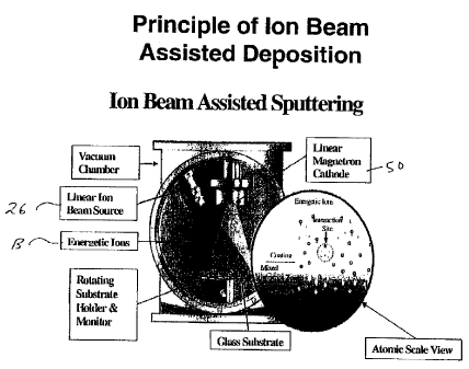
S3'in Fig. 1). Figs. 2(c) and 6 illustrate that in the IBAD type of ion beam
treatment/formation, both an ion beam source(s) 26 and a sputtering device
including
a sputtering target(s) 50 are used. An ion beam B from the ion beam source 26
intersects with the material M sputtered from the sputtering target(s) 50
proximate the
surface where the additional or remainder portion of the IR reflecting layer
is being
grown, so that the additional or remainder portion of the IR reflecting layer
is
grown/formed by a simultaneous combination of both the ion beam and
sputtering. In
certain example embodiments of this invention, a first Ag sputtering target is
used for
sputter-depositing the seed layer, and a second Ag sputtering target spaced
apart from
7
2? Acne 0604/2006
CA 02565444 2006-10-31
WO 2006/012184 PCT/US2005/022197
the first target is used to deposit/form the additional or remainder portion
of the IR
reflecting layer via IBAD.
[0030] The use of the seed layer and then the subsequent formation of the
additional or remaining portion of the IR reflecting layer (9 and/or 19) using
IBAD as
shown in Figs. 1-2 and 6 results in an IR reflecting layer that is graded with
respect to
argon content. In particular, an upper portion of the IR reflecting layer
includes a
higher Ar concentration than does a lower portion of the IR reflecting layer.
This is
because Ar ions do not impinge upon the layer during formation thereof until
after the
seed layer has been formed. Accordingly, the upper portion of the resulting IR
reflecting layer includes a higher Ar content than does the lower portion of
the layer.
This grading would be for content of another element (e.g., Kr and/or Xe) if
the other
element(s) was used instead of or in place of Ar in the ion beam in
alternative
embodiments of this invention. In certain example embodiments, the upper
portion of
the IR reflecting layer (9 and/or 19) has an argon (or other inert element)
concentration at least 10% higher than that of the lower portion of the IR
reflecting
layer, more preferably at least 20% higher, and most preferably at least 30%
higher.
The "lower portion" is merely some arbitrarily selected portion of the layer
at least
partially below the center point of the layer, where the "upper portion" of
the layer is
some arbitrarily selected portion of the layer at least partially above the
center of the
layer. In certain example instances, the upper portion may be the upper 20 A
of the
IR reflecting layer, and the lower portion may be the lower 60 A (or 20 A) of
the
layer.
[0031] Thus, the resulting IR reflecting layer (9 and/or 19) shown in Figs.
2(c)
and 3 is made up of the combination of the Ag inclusive seed layer and the Ag
inclusive layer formed immediately thereover via IBAD. Note that the seed
layer will
have been modified by the MAD process, with Ar ions having been injected
thereinto
and/or its stress having been changed from tensile to compressive. As
explained
above, it has surprisingly been found that: (a) the IBAD formation of the Ag
layer
portion of the seed layer in a suitable manner causes the stress of the seed
layer to
change from tensile to compressive in the final IR reflecting layer 9 and/or
19; and (b)
the IBAD formation of the additional Ag inclusive layer portion immediately
over and
8
CA 02565444 2006-11-01
Printed: 18/0512006 DESCPAMD - US0522197
contacting the seed layer results in an JR reflecting layer having improved
electrical
resistance properties and thus improved solar control functionality. -
[0032] Then, -following formation of the IR reflecting layer 9 and/or 19,
additional layer(s) are deposited on the substrate 1 over at least the IR
reflecting layer
(see step S4 in Fig. 1). These additional layer in the example Fig. 3
embodiment may
be layers 11-25 and/or 21-25.
[0033] In certain example embodiments, the resulting IR reflecting layer 9
and/or 19 has a thickness of from about 60 to 200 A, more preferably from
about 80
to 170 A, even more preferably from about 100 to 140 A, with an example being
about 120 A. Moreover, in certain example embodiments of-this invention, the
IR
reflecting layer(s) 9 and/or 19 are substantially free of oxygen. For.example,
the IR
reflecting layer(s) 9 and/or 19 include from about 0-10% oxygen, more
preferably
from about 0-5% oxygen, even more preferably from about 0-2% oxygen and most
preferably from 0-1% oxygen. This substantially free of oxygen characteristic
may be
achieved throughout the entire thickness, of the layer, or alternative in at
least a central
portion of the layer no located immediately adjacent the contact layers.
[0034] In certain example embodiments of this invention, the ion beam = =
includes at least ions from an inert gas used in the ion source 26. For
example, the ion
beam B may be of or include Ar+ ions if only Ar gas is used in the ion source
26. In
certain example embodiments of this invention, the ion beam is substantially
free of
oxygen ions and the gas used in the ion source 26 is substantially free of
oxygen.
Thus, the ion beam B and gas introduced into the ion source 26 include from 0-
10%
oxygen, more preferably from 0-5% oxygen, even more preferably from 0-2%
oxygen, and most preferably from 0-1% oxygen (0% oxygen may be preferred in
many instances). The ion beam is also substantially free of nitrogen ions in
certain
example embodiments of this invention.
[0035] Moreover, in certain example embodiments of this invention, in
forming the additional or remainder portion of the IR reflecting layer(s) 9.
and/or 19
via I33AD, an ion energy of from about 150 to 700 eV per Are ion, more
preferably of
from about 200 to 600 eV per Arm ion, and most preferably about 500 eV per At
ion
is used. As an example, when only Ar gas is used in the ion source 26, an
9
`'~, s..,.õ-= Amended S,'06/04/2006
CA 02565444 2009-04-27
WO 2006MI2184 PC IUS200S/022197
anodelcathode voltage of from about 30D to 1,400 V may be used at the source
26,
more preferably from about 400 to 1,200 V, and most preferably abort 1,000 V.
[0036] Ingure 3 is a side cm sectional view of a coated article according to
an example non-limiting embodiment of this invention. The coated article
includes
substrate I (e.g., clear. green, bronze. or blue-green glass substrate frost
about 1.0 to
10.0 mm thick, more preferably from about 1.0 mm to 3.5 mm thick), and a low-
'E
coaling (or layer system) 2 provided on the substrate I either dhecdy or
indirectly.
The costing (or layer system) 2 includes, in this example embodiment.
dielectric
silicon nitride layer 3 (wlricb may be ion beam treated) which may be of Si1N4
or or
any other suitable stoichioetry of silicon nitride in differs; t embodiments
of Ibis
ionventicm, first lower contact layer 7 (which contacts IR re eding layet 9),
That
conductive andprdccably metel1ic err t yblsily metallic infrared (1R)
reflecting
layer 9, first upper contact layer 11 (which contacts layer 9). dielectric
layer 13
(which may be deposited in one or multiple steps in different embodiments of
this
invention), another silicon nitride layer 14, second lower contact layer 17
(which
contacts IR reflecting layer 19), second conductive and pniferably metallic
3[f
reflecting layer 19. second upper contact layer 21 (which contacts layer 19).
dielectric
layer 23, and finally dielectric silicon nitride overcoat layer 25 (which may
be ion
beam treated). The "contact" layers 7,11,17 and 21 each contact at least one
1R
ref acting layer. The aforesaid layers 3-25 make up low-E (.e., low
emissivity)
coating 2 which is provided on glass or plastic substrate 1. Silicon nitride
layer 25 is
the outermost layer of the coating 2.
[0037] In embodiments herein discussing Ion beam treatment of Ile reflecting
layer, the ion beam tteatmerrtlformation maybe performed with respect to Ag
layers 9
aadlor 19.
[0038] In monolithic instances, the coated article includes only one glass
substrate 1 as illustrated In Fig. 3. however, monolithic coated articles
herein maybe
used in devices such as laminated vehicle windshieidi. 10 window units, and
the Mm.
A laminated vehicle window such as a windshield includes first and second
glass
substrates laminated to one another via a polymer based intedayer (e.g., see
US
6,686,050). One of these
CA 02565444 2009-04-27
WO 1006001219 PCI1IJ 2225 7
aubatrttes of the ltmmteae may srappet coadag 2 on an iettekr a+aface thaWis
certain example embodiment. As tar 10 wWow t ere I0 window unit may
include two spaced apart substrates 1. An example 10 window unit is
illustrated and
described, far example, is U.S. Patent No. 6,632,481.
An example m window xmit may imclade,,
for e:smp1c. the coated glens subsumes I ahem in ft 3 coogiled0a watberglsss
and Busse via spacer(s), sodsm d(s) or the litre with a gsp being defined
therebetween.
This sap between the substrata is 10 unit embodiments may in cataia imsta ces
be
fllicd with a ps such as argon (Ar). An exempla iG uelr may compass a pair of
spaced apart cleat glass substrates mash about 4 mm duck em of which is coated
with
a coatinghwin in certain example insttaves, wbare the gap betty the substtstee
may be fmm about 3 to 30 min. mm paferaUy floan sbout 10 to 20 mm and most:
pmfaably about 16 mm. In certain example instsm m the coating 2 may be
provided
on the mtedarsurfhca of tithersubstrate faring the gap.
(0039] Example detail" relating to layers 3,7,9,11, 13,14,17,19, 21,23 and
25 of the pig. 3 coxing are dicussed to U.S. Patent No. 7,344,782.
Per
etrsmple, ditdectdc layers 3 and 14 may be of or iuclttds a'lleon oiMde in
certain
emboc m s of chi inventlotz. Silicon astride layers 3 and 14 may, ammg other
things, improve heat-ttetaability of the cawed articles, e.g., auCh as thermal
tmaparing
or the life. The silicon rdtdde of layca 3 aadfcr 14 may be of the stole c
type
(813N4) type, uiumgan doped type doe to ion beans treslmeart dmof as discussed
haradrr, or aaaemadvely of dw Si-rich type in different embodiments of this
invention.
Any aadlor all of the sfcoa nitride layers discussed herein tray be doped with
other
mamdriab such as stainless steel or atmmbamm in cestain awcaple cmbadis t of
this
brna ion. Per agmpl, any andfor Aailic nuitcidebryen d adbadn may
Opel= allylacInds fray :boat 0-1396 shunimm now pefeaabiy from about 1 to 10%
aluminum, most pefcrably tram 14% aluminum, bn certain example embodiments of
this invention. The ailieoar nitride may be deposited by sputtering a target
of St or
3sAl In certain embodiments of this invention. Maseover, aEtcon nitride layer
3 may
be iaa balm treated in any sir discussed herein (e46 with at least nitrogen
ions
11
CA 02565444 2006-11-01
Printed. 18/05/2006'
DESCPAMD ` US0522197
via IBAD) in order to reduce sodium migration from the glass substrate toward
the IR
reflecting layer(s) during HT.
[0040] Infrared (IR) reflecting layers 9 and 19 are preferably substantially
or
entirely metallic and/or conductive, and may comprise or consist essentially
of silver
(Ag), gold, or any other suitable IR reflecting material. One or both of IR
reflecting
layers 9 and/or 19 may be formed by the ion beam inclusive techniques as
discussed
herein with respect to Figs. 1-2. IR reflecting layers 9 and 19 help allow the
coating
to have low-E and/or good solar control characteristics. The IR reflecting
layers may,
however, be slightly oxidized in certain embodiments of this invention.
[0041] Dielectric layer 13 may be of or include tin oxide in certain example
embodiments of this invention. However, as with other layers herein, other
materials
may be used in different instances. Lower contact layers 7 and/or 17 in
certain
embodiments of this invention are of or include zinc oxide (e.g., ZnO). The
zinc
oxide of layer(s) 7, 17 may contain other materials as well such as Al (e.g.,
to form
ZnAlO.,). For example, in certain example embodiments of this invention, one
or
more of zinc oxide layers 7, 17 may be doped with from about 1 to 10% Al, more
preferably from about 1 to 5% Al, and most preferably about 2 to 4% Al. The
use of
zinc oxide 7, 17 under the silver 9, 19 allows for an excellent quality of
silver to be
achieved. Upper contact layers 11 and/or 21 may be of or include. NiCr, NiCrOQ
and/or the like in different example embodiments of this invention.
[0042] Dielectric layer 23 may be of or include tin oxide in certain example
embodiments of this invention. However, layer 23 is optional and need not be
provided in certain example embodiments of this invention. Silicon nitride
overcoat
layer 25 may be initially deposited by sputtering or SAD, and may be ion beam
treated in any manner discussed herein.
(00431 Other layer(s) below or above the illustrated coating may also be
provided. Thus, while the layer system or coating is "on" or "supported by"
substrate
=1 (directly or indirectly), other layer(s) may be provided therebetween.
Thus, for-
example, the coating of Fig. 3 may.be considered "on" and "supported by" the
substrate I even if other layer(s) are provided between layer 3 and substrate
1.
Moreover, certain layers of the illustrated coating may be removed in certain
12
4 Amended Si,aPt
1.06J04/2006
E:o-_
CA 02565444 2006-10-31
WO 2006/012184 PCT/US2005/022197
embodiments, while others may be added between the various layers or the
various
layer(s) may be split with other layer(s) added between the split sections in
other
embodiments of this invention without departing from the overall spirit of
certain
embodiments of this invention.
[0044] Fig. 7 is a flowchart illustrating how an IR reflecting layer 9 and/or
19
may be formed according to another example embodiment of this invention. In
the
Fig. 7 embodiment, an IR reflecting layer may be formed entirely using IBAD.
At the
beginning of the IR reflecting layer formation using IBAD, the volts applied
to the ion
source are low or zero so that the ion beam either is not formed or is of a
low energy
type (i.e., low eV per ion). Then, during formation of the IR reflecting layer
after at
least some of the layer has been deposited, the voltage at the ion source is
increased
so as to increase the eV per ion in the ion beam. In other words, the ion
energy is
increased, either progressively or in a step-like manner, during formation of
the IR
reflecting layer. This prevents or reduces damage to the lower portion of the
IR
reflecting layer and/or to the layer under the same since a low energy ion
beam is used
to form the initial part of the IR reflecting layer, and yet achieves the
advantages
discussed herein with respect to the final IR reflecting layer since a higher
energy is
used to form at least the upper portion of the IR reflecting layer.
[0045] Referring in detail to Fig. 7, one or more underlying layer(s) are
deposited on substrate 1 (ST1). This step is similar to step Si in the Fig. 1
embodiment. Then, during the deposition of the first portion of the IR
reflecting layer
(9 and/or 19), IBAD is used but the ion beam is characterized by a relatively
low
energy (ST2). For example, in ST2 during the formation of the initial portion
of the
IR reflecting layer, an ion energy of from about 0 to 200 eV per Ar' ion, more
preferably from about 1 to 150 eV, more preferably from about 5 to 100 eV per
Arl
ion is used. Again, other inert gas(es) may be used instead of or in addition
to argon.
Then, after part of the IR reflecting layer has been formed, the ion energy is
increased
for forming the additional or remainder portion of the IR reflecting layer(s)
9 and/or
19 via IBAD (ST3). In certain example embodiments, the ion energy is increased
to
an ion energy of from about 150 to 700 eV per Ar+ ion, more preferably of from
about
200 to 600 eV per Ar+ ion, and most preferably about 500 eV per Ar+ ion in
ST3. In
13
CA 02565444 2006-10-31
WO 2006/012184 PCT/US2005/022197
certain example embodiments of this invention, the ion energy is increased by
at least
about 10% in step ST3, more preferably at least about 25%, even more
preferably at
least about 50%, sometimes at least about 100%. After the additional and/or
remainder portion of the IR reflecting layer has been formed using the higher
ion
energy, additional layer(s) are deposited/formed on the substrate 1 over at
least the IR
reflecting layer (ST4).
[0046] While various thicknesses and materials may be used in layers in
different embodiments of this invention, example thicknesses and materials for
the
respective layers on the glass substrate 1 in the Fig. 3 embodiment are as
follows,
from the glass substrate 1 outwardly. One or both of the IR reflecting layers
9 and/or
19 are formed/deposited using at least IBAD according to any of the
embodiments
discussed herein.
Example Materials/Thicknesses; Fig. 3 Embodiment
Layer Preferred Range (A) More Preferred (A) Example (A)
Glass (1-10 mm thick)
Si3N4 (layer 3) 40-450 A 70-250 A 100
ZnO, (layer 7) 10-300 A 40-150 A 100
Ag (layer 9) (IBAD) 50-250 A 80-120 A 98
NiCrO,, (layer 11) 10-100 A 30-45 A 35
Sn02 (layer 13) 0-1,000 A 350-630 A 570
SiXNy (layer 14) 50-450 A 90-150 A 120
ZnO,, (layer 17) 10-300 A 40-150 A 95
Ag (layer 19)(IBAD) 50-250 A 80-220 A 96
NiCrO,, (layer 21) 10-100 A 30-45 A 35
Sn02 (layer 23) 0-750 A 150-300 A 200
Si3N4 (layer 25) 10-750 A 100-320 A 180
[0047] Optionally, one or both of silicon nitride inclusive layers 3 and/or 25
may be ion beam treated in certain example embodiments of this invention. Ion
beam
treatment of silicon nitride inclusive layer 3 has surprisingly been found to
reduce
sodium migration during optional heat treatment thereby improving coating
14
CA 02565444 2006-10-31
WO 2006/012184 PCT/US2005/022197
characteristics, whereas ion beam treatment of silicon nitride overcoat layer
25 has
been found to improve durability of the resulting coated article. The ion beam
treatments of layer(s) 3 and/or 25 may be performed with either via IBAD using
nitrogen ions from at least nitrogen gas in the ion source, and/or via so-
called peening
where an ion source directs at least nitrogen ions at the layer after
sputtering thereof.
[0048] In different embodiments of this invention, the ion beam treatment of a
silicon nitride inclusive layer 3 and/or 25 may be performed: (a) while the
layer is
being sputter-deposited, and/or (b) after the layer has been sputter-
deposited. The
latter case (b) may be referred to as peening, while the former case (a) may
be referred
to as ion beam assisted deposition (IBAD) in certain example instances. IBAD
embodiments (e.g., see Fig. 8) are particularly useful for unexpectedly
causing a
deposited layer to realize anti-migration characteristics regarding sodium
migration
relating to layer 3. However, post-sputtering ion beam treatment (or peening)
may
also be used in any ion beam treatment embodiment herein. In certain example
embodiments of this invention, ion beam treatment is performed in a manner so
as to
cause part or all of a silicon nitride inclusive layer 3 and/or 25 to become
nitrogen-
rich (N-rich). In such embodiments, dangling Si bonds are reduced or
eliminated, and
excess nitrogen is provided in the layer (e.g., see layer 3 and/or 25). This
may in
certain instances be referred to as a solid solution of N-doped silicon
nitride. Thus, in
certain example instances, the layer(s) 3 and/or 25 may comprise Si3N4 which
is
additionally doped with more nitrogen. In certain example embodiments, the
Si3N4
may be doped with at least 0.1% (atomic %) nitrogen, more preferably from
about 0.5
to 20% nitrogen, even more preferably from about 1 to 10% nitrogen, and most
preferably from about 2 to 10% nitrogen (or excess nitrogen). In certain
example
instances, the nitrogen doping may be at least about 2% nitrogen doping.
Unlike the
nitrogen in the Si3N4 of the layer, the excess nitrogen (or the doping
nitrogen
referenced above) is not bonded to Si (but may or may not be bonded to other
element(s)). This nitrogen doping of Si3N4 may be present in either the entire
layer
comprising silicon nitride, or alternatively in only a part of the layer
comprising
silicon nitride (e.g., proximate an upper surface thereof in peening
embodiments).
Surprisingly, it has been found that this excess nitrogen in the layer (i.e.,
due to the N-
doping of Si3N4) is advantageous in that it results in less structural
defects, reduced
CA 02565444 2006-10-31
WO 2006/012184 PCT/US2005/022197
sodium migration during optional heat treatment when used in a layer under an
IR
reflecting layer(s), and renders the layer less reactive to oxygen thereby
improving
durability characteristics. In certain example embodiments of this invention,
at least
nitrogen (N) ions are used to ion treat a layer(s) comprising silicon nitride.
In certain
example embodiments, using an ion beam treatment post-sputtering (i.e.,
peening),
such an ion beam treatment may include utilizing an energy of at least about
550 eV
per N2+ ion, more preferably from about 550 to 1,200 eV per N2+ ion, even more
preferably from about 600 to 1100 eV per N2+ ion, and most preferably from
about
650 to 900 eV per N2+ ion (an example is 750 eV per N2+ ion). It has
surprisingly
been found that such ion energies permit excellent nitrogen grading
characteristics to
be realized in a typically sputter-deposited layer of suitable thickness,
significantly
reduce the number of dangling Si bonds at least proximate the surface of the
layer
comprising silicon nitride, provide improved stress characteristics to the
coating/layer,
provide excellent doping characteristics, reduce the potential for sodium
migration,
and/or cause part or all of the layer to become nitrogen-rich (N-rich) which
is
advantageous with respect to durability. Possibly, such post-sputtering ion
beam
treatment may even cause the stress of the layer to change from tensile to
compressive
in certain example instances. In IBAD embodiments where the ion beam treatment
is
performed simultaneously with sputtering of the layer 3 and/or 25, it has
surprisingly
been found that a lower ion energy of at least about 100 eV per N2+ ion, more
preferably of from about 200 to 1,000 eV per N2+ ion, more preferably from
about 200
to 600 eV per N2+ ion, still more preferably from about 300 to 500 eV per N2+
ion
(example of 400 eV per N2+ ion) is most suitable at the surface being treated.
It has
surprisingly been found that such ion energies in IBAD embodiments
significantly
reduce the number of dangling Si bonds, provide improved stress
characteristics to the
coating/layer, provide excellent doping characteristics, reduce sodium
migration
during heat treatment, and/or cause part or all of the layer to become
nitrogen-rich (N-
rich) which is advantageous with respect to durability. It has surprisingly
been found
that this ion energy range is especially beneficial in causing the silicon
nitride layer 3
and/or 25 to realize compressive stress and/or prevent or reduce sodium
migration
during optional heat treatment. If the ion energy is too low, then the layer
will not
densify sufficiently. On the other hand, if the ion energy is too high, this
could cause
16
CA 02565444 2006-10-31
WO 2006/012184 PCT/US2005/022197
damage to the layer and/or cause the stress of the treated layer to flip to
tensile. Thus,
this ion energy range provides for unexpected and advantageous results. In
certain
example instances, it has surprisingly been found that the ion treatment of
layer 3
and/or 25 may improve durability, heat treatability and/or coloration
characteristics of
the coated article by at least one of: (i) creating nitrogen-doped Si3N4 in at
least part
of the layer, thereby reducing Si dangling bonds and susceptibility to sodium
migration upon heat treatment; (ii) creating a nitrogen graded layer in which
the
nitrogen content is greater in an outer portion of the layer closer to the
layer's outer
surface than in a portion of the layer further from the layer's outer surface;
(iii)
increasing the density of the layer which has been ion beam treated, (iv)
using an ion
energy suitable for causing the stress characteristics of the layer to be
improved; (v)
improving stoichiometry control of the layer, (vi) causing the layer to be
less
chemically reactive following ion treatment thereof, (vii) causing the layer
to be less
prone to significant amounts of oxidation following the ion treatment, and/or
(viii)
reducing the amount and/or size of voids in the layer which is ion treated. In
certain
example embodiments of this invention, the ion treatment is treatment using an
ion
beam from at least one ion source, where Ar, or Ar and N ions are preferred.
[0049] In certain IBAD embodiments, if the appropriate ion energy is used for
a given material, the compressive stress of the IBAD-deposited layer 3, 9, 19,
and/or
25 may be from about 50 MPa to 2 GPa, more preferably from about 50 MPa to 1
GPA, and most preferably from about 100 MPa to 800 MPa. Such IBAD techniques
may be used in conjunction with IR reflecting layer(s), base layer(s),
overcoat layer(s)
or any other layer herein which may be ion beam treated.
[0050] In various embodiments discussed herein, the ion beam may be a
focused ion beam, a collimated ion beam, or a diffused ion beam in different
embodiments of this invention.
[0051] Coated articles according to different embodiments of this invention
may or may not be heat treated (HT) in different instances. The terms "heat
treatment" and "heat treating" as used herein mean heating the article to a
temperature
sufficient to achieve thermal tempering, heat bending, and/or heat
strengthening of the
glass inclusive article. This definition includes, for example, heating a
coated article
17
CA 02565444 2009-04-27
WO 2001ID12194 PCT11732405/e221n7
in an even or ata of bog about 5 O degmore pizinibly
at last about 606 doges C, for a sufficient period to allow aempetiug, ba beg,
msdlor beatagog biomtsia htsttanoee, sheHI' may begotatleast sbo ot4 a
S minutes. in certain example ambodmots of this invention, ion beams treated
silicon nitride wdernoat aadlar overcoat layers me advmdPoaa in i4s4 they
chums
less with legasd to color asldlor trassniasion dudeg optional heat treatment,
this can
improve layer a lhedon and thus duty of the final pradnct and Ice beam
treated lower silicon nitride inclusive layers aid in reduction of sodium
migration
during Sr.
C0132] II is noted that any of the sileoa nitride layers 3 aodlar 2S to be ion
beam treated herein may be initially sputter deposited is any saietbte s
aoiehiometric
fans ioaluding but not limited to S1 N4 or 4 Sf-tick type of Mon nitride.
Example
Si-rich types of silicon nitdda eta dhecmwed in U.S. 200210064662
(incorporated
herein by refesssce), and any 51-dch layer discussed tbernein maybe initially
Wow
depoaNDd herein for any suitable O cm nitride lays. Also, dB= rdtdde layers
herein may of cause be doped with aluminum (e.g., 1-10%) or the Mm in certain
example embodhaeas of this invention. It has also been found that km beam
twat4ng
of a layerG . a ng shorn nitride (3 aasffor 25) Increases the hard son of such
a
layer as lag to certain rode ambodimeaft of this utveatan (e.g., via IBAD or
peening). A layer eoun ridng s illaam nitride when conventionally read
typically
has a hardness of from 10.14 flea. h- ttain examp1 smbodimdnta of this Irmadon
however, when ion beam treated, the Mom vitxide layer C3 and/or 25) realizan a
hsrdms of at least 20 OPt, more pradmably of at least 22 OPa, and most p
olombly
of at least 24 OPt,
10133] In certain example embodiments of this inventiao. one or both of NiCr
or NICuO 1 layers I i aad/ar 21 may be ion beam treated retina at least oxygen
ions in
order to oxidation V "e as described hr US. Patent Application Me. 200"25M9-
10"Q Figures 4S illustrate an exemplary linear or direct ion beam source 26
which maybe used to tam the addticsad oriemneindarpordonof an 1R refiecoln`
layer (9 and/or 19) as discussed above In connection with Figs. 1-3, or to ion
beam
la
CA 02565444 2009-04-27
WO 2N 121$4 PCTAUS200SIO22197
Unit layer(s) 3 a udrar 25 with at last nitrogen lama in certain example
embodiments
of this inve an (viapeenlag err ]BAD). Z'm bean aaunce (or iaa Source)
26lndudes
pa/power inlet 31, racetrack-shaped anode 27, gR ended cathode magnet portion
28.
ma natpolee, and bnolat= 30. An electric Sepia drgiaedbetweem fire anode 27
and
the cathode 29. A 3kV n any other suitable DC power supply may be used for
source
26 in acme embodiments. The gse(es) der sad hare~us foe lane is that ion sou
ce
during the ion beam treatment may be introduced into t e source via gas inlet
31, cc
via any other suitable location. Ion beam aosace 26 is based upon a known $
idteas
ion not design. The linear somas may include a linear shell (which ie the
caihode
and grwnded) inside of which lies a concentric anode (which is at a positive
potesalel). This p maetry of ashndereaode nmpdk $,eld33 may givetse to a
close drift cos tiom. freedetock gaea (e.g., ukrog m, age, a miattime of
nitrogen and
argon, etc.) maybe tad through to cavity 41 between the anode 27 and cathode
29.
The electrical energy between the anode and cathode cracks the gas to produce
a
plasma within de source. The lane 34 (e.g, nitrogen lam) we eatpelled out
(e.g., as
to the nitrogen gas in the source) and directed twrard the layer to be Ion
beam
treated/formed in the form of an ion beam. The ion beam may be diffoaued,
coIGmatr d, orfocuec& Bxample ions 34 in beam (B) ate shown in Figure 4.
(0055] A linear source as long as 0.3 to 41nelu, maybe made sad fused in
d rain example imta et alih-ani¾s sources tk lc ngtbs ate wheel ate din
dlfho t embodiments of this invealon. Blectroe layer 33 is shown in Figure 4
and
completes the chu t thereby pmmhtmg the icon bceme oe to fimctiop openly.
. Example but am-limiting k e beam sources that maybe used are disclosed
inU.S.
Patent Document Noe. b,303.226.6,359,388, and/or 2OO4f0067363 ,
[0056] In, ertain example embodin is of this Invention, coated article
herein having two IR reflecting layer 9,19 may have the following optical and
solar
ciiaractedat ca when meamcd monolithically (beftxe my eptionsl H!). The sheet
resistances ( herein taka into account all lR rsIletaing layers (e.g., silver
layeta 9.
19).
19
CA 02565444 2006-10-31
WO 2006/012184 PCT/US2005/022197
Optical/Solar Characteristics (Monolithic double-Ag; pre-HT)
Characteristic General More Preferred Most Preferred
RS (ohms/sq.): <= 5.0 <= 3.5 <= 2.5
Ea: <= 0.08 <= 0.03 <= 0.025
T,,,, (Ill. C 2 ): >= 70% >= 75% >= 75.5%
[0057] In certain example embodiments, coated articles herein may have the
following characteristics, measured monolithically for example, after heat
treatment
):
Optical/Solar Characteristics (Monolithic double-Ag; post-HT)
Characteristic General More Preferred Most Preferred
RS (ohms/sq.): <= 5.0 <= 3.0 <= 2.0
Eõ: <= 0.07 <= 0.03 <= 0.0025
T,,1 (Ill. C 2 ): >= 70% >= 75% >= 80%
Haze: <= 0.40 <= 0.35 <= 0.30
[0058] It is noted, however, that for coatings having only one IR reflecting
layer, the sheet resistance and emissivity values will of course be higher.
[0059] Moreover, in certain example laminated embodiments of this
invention, coated articles herein which have been heat treated to an extent
sufficient
for tempering and/or heat bending, and which have been laminated to another
glass
substrate, may have the following optical/solar characteristics:
Optical/Solar Characteristics (Laminated double-Ag; post-HT)
Characteristic General More Preferred Most Preferred
RS (ohms/sq.): <= 5.0 <= 3.0 <= 2.0
Eõ: <= 0.07 <= 0.03 <= 0.025
T,j (Ill. D65 10 ): >= 70% >= 75% >= 77%
Haze: <= 0.45 <= 0.40 <= 0.36
[0060] Moreover, coated articles including coatings according to certain
example embodiments of this invention have the following optical
characteristics
(e.g., when the coating(s) is provided on a clear soda lime silica glass
substrate 1 from
CA 02565444 2006-10-31
WO 2006/012184 PCT/US2005/022197
1 to 10 mm thick; e.g., 2.1 mm may be used for a glass substrate reference
thickness
in certain example non-limiting instances) (laminated).
Example Optical Characteristics (Laminated double-Ag: post-HT)
Characteristic General More Preferred
T,j (or TY)(Ill. D65 10 ): >= 75% >= 77%
a*t (Ill. D65 10 ): -6 to +1.0 -4 to 0.0
b*t (Ill. D65 10 ): -2.0 to +8.0 0.0 to 4.0
L* (Ill. D65 10 ): 88-95 90-95
RfY (Ill. C, 2 deg.): 1to12% 1to10%
a*f (Ill. C, 2 ): -5.0 to +2.0 -3.5 to +0.5
b*f (111. C, 2 ): -14.0 to +10.0 -10.0 to 0
L* (Ill. C 2 ): 30-40 33-38
RgY (Ill. C, 2 deg.): 1 to 12% 1 to 10%
a*g (Ill. C, 2 ): -5.0 to +2.0 -2 to +2.0
b*g (Ill. C, 2 ): -14.0 to +10.0 -11.0 to 0
L* (Ill. C 2 ): 30-40 33-38
[0061] The following examples are provided for purposes of example only
and are not intended to be limiting.
EXAMPLES
[0062] In Example 1, an IR reflecting layer of Ag was formed on a 100 A
thick ZnO layer. In forming the IR reflecting layer, an Ag seed layer about 60
A thick
was first deposited via sputtering, and thereafter the remainder of the IR
reflecting
layer was formed using IBAD. The IBAD, at room temperature, utilized a silver
sputtering target and an ion beam of argon ions, where the average ion energy
was
from about 200 to 250 eV per Ar+ ion.
[0063] Comparative Example 1 was the same as Example 1 above, except that
the entire Ag IR reflecting layer was formed using only sputtering (no MAD was
used). The results comparing Example I and Comparative Example are set forth
below.
21
CA 02565444 2006-11-01
Printed:. 18/0512006 DES'CPAMD
US0522197
Ex. 1 Comparative Ex. 1
Ag Thickness (total): 120 A 120 A
Sheet Resistance (RS, ohms/square): 3.0 3.8
IBAD: yes no
Ion Energy per Ar+ ion: 200-250 eV 0
Stress Type: compressive tensile
[0064] It can be seen from the above that the use of IBAD (see Example 1) in
helping form, the IR reflecting layer resulted in a significantly improved
(i.e., lower)
sheet resistance of the IR reflecting layer.. Indeed, the sheet resistance
(R5) was about
21% lower in Example 1 where IBAD was used, than in Comparative Example 1
where only sputtering was used to form the IR reflecting layer (3.8 - 3.0 =
0.8; and
0.813.8 = 21%). In certain example embodiments of this invention, the use of
IBAD
causes the sheet resistance (RS) to be at least about 5% lower than if ion
beam
treatment such as IBAD had not been used, more preferably at least about 10%
lower,
sometimes at least 15% lower, and even at least 20% lower in certain
instances.
Moreover, the compressive stress of the IR reflecting layer of Example 1
resulted in
significantly improved durability compared to Comparative Example 1, since
Comparative Example 1 had tensile stress due to its deposition using only
sputtering.
[0065] In Example 2,- an 1R reflecting layer of Ag about 139 A thick was
formed on a 600 A thick ZnO layer. In forming the IR reflecting layer, an Ag
seed
layer portion about 60 A thick was first deposited via sputtering, and
thereafter the
remainder of the IR reflecting layer was formed using IBAD. The IBAD, at room
temperature, utilized a silver sputtering target and an ion beam of argon
ions, where
the average ion energy was about 250 eV per Are' ion.
[0066] Comparative Example 2 was the same as Example 2, except that the
entire Ag IR reflecting layer was formed using sputtering without IBAD.
[0067)= Comparative Example 3 did not include a seed layer, and instead used
I]BAD at the same ion energy to deposit the entire Ag IR reflecting layer.
Amended
' , ; 06/04/2006=;
CA 02565444 2006-10-31
WO 2006/012184 PCT/US2005/022197
Ex. 2 Comp Ex. 2 Comp Ex. 3
Ag Thickness (total): 139 A 153 A 144 A
Bulk Resistivity [ S2 cm]: 4.6 4.8 4.9
Seed layer yes no no
IBAD: yes no yes
Ion Energy per Ar+ ion: 250 eV 0 250 eV
Stress Type: compressive tensile compressive
[0068] It can be seen from the above that the use of IBAD (see Example 2) in
helping form the IR reflecting layer resulted in an improved (i.e., lower)
resistance of
the IR reflecting layer compared to only sputtering in Comparative Example 2.
It is
noted that the bulk resistance (BR) in the chart above can be converted to
sheet
resistance as follows: RS = BRJd, where "d" is the thickness of the JR
reflecting layer.
Moreover, the compressive stress of the IR reflecting layer of Example 2
resulted in
significantly improved durability compared to Comparative Example 2, since
Comparative Example 2 had tensile stress due to its deposition using only
sputtering.
[0069] The comparison between Example 2 and Comparative Example 3
illustrates the benefit of the Ag seed layer. In particular, when the seed
layer was not
present and the same rather high ion energy was used to deposit the entire Ag
IR
reflecting layer via IBAD, the electrical resistivity actually was worse
(higher) than
with only sputtering (compare Comparative Example 3 with Comparative Example
2). It is believed that this occurred since the high ion energy used at the
beginning of
forming the IR reflecting layer caused significant ion mixing with the
underlying ZnO
and thereby damaged the structure of the resulting JR reflecting layer. This
illustrates
the advantage of the Fig. 7 embodiment where IBAD can be used to form the
entire
IR reflecting layer, except that ion energy is increased during deposition of
the layer
so that such damage to lower portions of the layer does not occur or is
reduced.
[00701 The following examples relate to ion beam treatment (either via IBAD
or peening) of silicon nitride layer (e.g., layers 3 and/or 25 for example and
without
limitation).
23
CA 02565444 2006-10-31
WO 2006/012184 PCT/US2005/022197
[0071] Examples 3-5 illustrate example techniques for forming layers 3 and/or
25, or any other suitable layer according to example embodiments of this
invention.
Examples 3-5 utilized IBAD type of ion beam treatment, and were made and
tested as
follows. A silicon nitride layer was deposited on a quartz wafer (used for
ease of
stress testing) using IBAD (e.g., see Fig. 6) under the following conditions
in the
deposition chamber: pressure of 2.3 mTorr; anode/cathode ion beam source
voltage
of about 800 V; Ar gas flow in the ion source of 15 sccm; N2 gas flow in the
ion
source 26 of 15 sccm; sputtering target of Si doped with about 1% boron; 460 V
applied to sputtering cathode; 5.4 sputtering amps used; 60 sccm Ar and 40
sccm N2
gas flow used for sputtering gas flow; linear line speed of 50 inches/minute;
where the
quartz wafer substrate was circular in shape and about 0.1 to 0.15 mm thick.
The ion
beam treatment time for a given area was about 3 seconds.
[0072] Example 4 was the same as Example 3, except that the anode/cathode
voltage in the ion source was increased to 1,500 V.
[0073] Example 5 was the same as Example 3, except that the anode/cathode
voltage in the ion source was increased to 3,000 V.
[0074] The stress results of Examples 3-5 were as follows, and all realized
compressive stress:
Example Compressive Stress Ion Source Anode/Cathode Volts
3 750 MPa 800 V
4 1.9 GPa 1,500 V
1 GPa 3,000 V
[0075] It can be seen from Examples 3-5 that the compressive stress of the
silicon nitride layer realized due to IBAD deposition is a function of ion
energy (i.e.,
which is a function of voltage applied across the anode/cathode of the ion
source 26).
In particular, 1,500 anode-cathode volts caused the highest compressive stress
to be
realized, whereas when too much voltage was applied the stress value began
moving
back toward tensile.
24
CA 02565444 2006-10-31
WO 2006/012184 PCT/US2005/022197
EXAMPLE 6
[0076] Example 6 used post-sputtering peening type of ion beam treatment,
and was made and tested as follows. A silicon nitride.layer about 425 A thick
was
deposited by conventional magnetron-type sputtering using a Si target doped
with Al
on a substrate. After being sputter-deposited, the silicon nitride layer had a
tensile
stress of 400 MPa as tested on the quartz wafer. After being sputter-
deposited. and
stress tested, the silicon nitride layer was ion beam treated using an ion
source 26 as
shown in Figs. 4-5 under the following conditions: ion energy of 750 eV per N
ion;
treatment time of about 18 seconds (3 passes at 6 seconds per pass); and N2
gas used
in the ion source. After being ion beam treated, the silicon nitride layer was
again
tested for stress, and had a tensile stress of only 50 MPa. Thus, the post-
sputtering
ion beam treatment caused the tensile stress of the silicon nitride layer to
drop from
400 MPa down to 50 MPa (a drop of 87.5%).
EXAMPLE 7
[00771 The following hypothetical Example 7 is provided for purposes of
example only and without limitation, and uses a 2.1 nun thick clear glass
substrates so
as to have approximately the layer stack set forth below and shown in Fig. 3.
The
layer thicknesses are approximations, and are in units of angstroms (A).
Layer Stack for Example 7
Layer Thickness (A)
Glass Substrate
N-doped Si3N4 100
ZnAlOX 109
Ag 96
NiCrOX 25
Sn02 535
SiXNy 126
ZnAlOX 115
Ag 95
NiCrOx 25
SnO2 127
CA 02565444 2006-10-31
WO 2006/012184 PCT/US2005/022197
N-doped Si3N4 237
[0078] The processes used in forming the coated article of Example 7 are set
forth below. The sputtering gas flows (argon (Ar), oxygen (0), and nitrogen
(N)) in
the below table are in units of sccm (gas correction factor of about 1.39 may
be
applicable for argon gas flows herein), and include both tuning gas and gas
introduced
through the main. The line speed was about 5 m/min. The pressures are in units
of
mbar x 10"3. The silicon (Si) targets, and thus the silicon nitride layers,
were doped
with aluminum (Al). The Zn targets in a similar manner were doped with about
2%
Al. IBAD was used in forming each of the Ag IR reflecting layers, and also for
the
upper and lower silicon nitride layers.
Sputtering Process Used in Example 7
Cathode Target Power(kW) Ar 0 N Volts Pressure
IBAD N-doped Si3N4 layer 3 formed using any of Examples 3-6
C14 Zn 19.5 250 350 0 276 2.24
C15 Zn 27.8 250 350 0 220 1.88
C24 Process of any of Examples 1-2
C25 NiCr 16.5 350 0 0 510 2.33
C28 Sn 27.3 250 454 350 258 2.30
C29 Sn 27.3 250 504 350 246 1.97
C39 Sn 30 250 548 350 257 2.29
C40 Sn 28.5 250 458 350 245 2.20
C41 Sn 30.8 250 518 350 267 2.45
C43 Si 59.7 350 0 376 285 2.47
C45 Zn 26.9 250 345 0 209 3.78
C46 Zn 26.8 250 345 0 206 1.81
C49 Process of any of Examples 1-2
C50 NiCr 16.6 250 75 0 575 1.81
C54 Sn 47.3 250 673 350 314 1.92
IBAD N-doped Si3N4 layer 25 formed using any of Examples 3-6
26
CA 02565444 2006-10-31
WO 2006/012184 PCT/US2005/022197
[0079] It can be seen that in the aforesaid Example 7 both of silicon nitride
layers 3 and 25 were ion beam treated in a manner so as to cause N-doping of N-
doped Si3N4 to occur in each of the layers, and both of the IR reflecting
layers were at
least partially formed using IBAD.
[0080] After being sputter deposited onto the glass substrates, the
hypothetical
Example 7 coated article was heat treated in a manner sufficient for tempering
and
heat bending, and following this heat treatment had the following
characteristics as
measured in monolithic form.
Characteristics of Example 7 (Monolithic; post - HT)
Characteristic Example 7
Visible Trans. (T,;, or TY)(Ill. C 2 deg.): 80.0%
a* -4.8
b* 10.7
Glass Side Reflectance (RY)(Ill C, 2 deg.): 8.3%
a* -3.5
b* 7.8
Film Side Reflective (FY)(Ill. C, 2 deg.): 7.5%
a* -5.8
b* 14.2
RS (ohms/square) (pre-HT): 2.74
RS (ohms/square) (post-HT): 2.07
Haze: 0.28
[0081] The coated article of Example 7 was then laminated to another
corresponding heat treated and bent glass substrate to form a laminated
vehicle
windshield product. Following the lamination, the resulting coated article
laminate
(or windshield) had the following characteristics.
Characteristics of Example 7 (Laminated; post - HT)
Characteristic Example 7
Visible Trans. (T,,15 or TY)(lll. D65 10 ): 77.8%
a* -3.1
27
CA 02565444 2009-04-27
WO 20661012184 PIQ820a61022197
b* 33
Glass Side R tce (RYXIU C, 2 des )-. 9.0%
a* 1.5
b* -9.1
Palm Me Reflective CM M C, 2 deg): 8.9%
b* -7.8
Rs (ohmalaquace) see above
l3aso: 0.32
(0 8Z1 While the aforesaid Examples ion beam treat Layers comprising sill
con
nitride and/or silver, this invention is not so limited. Oder layers maybe ion
beam
toad ia a similermaoner.
[00837 In certain other etUaliment of this invention, any of the afatizsaid
embodfhneotamay be spphed t other . Por example and without limitwdon,
any of the; a enld embodiments may also be applicdto coated articles and than
solar
control coatings close of moss of U.S. PO M Doament Nos . 2A03R /5071 t,
200310194570.6.723.211.6.576.349.5.514.476.5.425,861.
[00841 While many of the above- lismdembodimantn arse used in the conmrt of
coated suites with solar control coatings, this invention is not so sited. For
exempla, ion beam treating of lsyem as iaceued herein may also be used in the
comma of other types of product and costiop relatingterato.
[00831 While the invention has been described in connection with what is
prsaot;y aonddered lobe the most practical sadpW6aed ambodBmmt, it is to be
understood theft invention is not to be limited to the disclosed embodiment,
but anti
the coney, is intended to cover various m ons and equivalent arrangements
in cis edwit in the spirit and scope of the appea,dad claims.
28