Note: Descriptions are shown in the official language in which they were submitted.
CA 02565453 2006-10-26
WO 2005/104743
PCT/US2005/014380
1
TITLE: ADAPTIVE GATE DRIVE FOR SWITCHING DEVICES OF
INVERTER
FIELD OF THE INVENTION
This disclosure generally relates to an adaptive gate drive for semiconductor
power
devices and more particularly relates to an adaptive gate drive for an
Insulated Gate Bipolar
Transistor for controlling the turn-on and/or turn-off behavior.
BACKGROUND OF THE INVENTION
Semiconductor power switching . devices, such as Insulated Gate Bipolar
Transistors (IGBTs) or Metal-Oxide-Semiconductor Field-Effect-Transistor
(MOSFETs)
are well-known in the art. For example, IGBTs have been the main power
semiconductors used in the inverter sections of variable speed AC motor drives
and other
similar .applications. The latest generation of IGBTs includes Trench Gate
Field Stop .
IGBT devices (TG-IGBTs), which are also sometimes referred to as third
generation
IGBT devices.
The trench gate IGBT devices offer substantial advantages over prior IGBT
devices. For example, the trench gate IGBT tends to have a lower on-state
voltage
requirement. Further, the trench gate IGBT is typically capable of faster
on/off switching
.than other semiconductor devices, including prior generations of IGBT
devices.
However, the very fast turn-off behavior of the trench gate IGBT device can
make
= maintaining the voltage across the IGBT within the Reverse Bias Safe
Operating Area
(RBSOA) very difficult. Additionally, the fast turn-off behavior of the trench
gate IGBT
. .
= device can cause, parasitic oscillations within connected circuits. Such
parasitic
.
oscillations can interfere with an/or cause failure of the gate drive and
other control
circuits. Moreover, when a free wheel diode. is used, as may be common in the
inverter
section of an Ac motor controller, the very fast turn-on behavior of the
trench gate IGBT
can cause problems with the reverse recovery. For example, the reverse
recovery during
"turn on" can=be very "snappy" because the current during reverse recovery
terminates
with a high rate of change. This can also cause parasitic oscillations and
potential failure
of the trench gate IGBT device and gate drive circuit: Such problems are more
=
significant at higher operating voltages and currents.
=
CA 02565453 2006-10-26
WO 2005/104743 PCT/US2005/014380
2
A number of techniques have been proposed in the art to address some of the
issues related to the fast turn-on and turn-off behavior of the trench gate
IGBT when used
in an inverter. In one technique, the gate resistance of the trench gate IGBT
is increased
so that the device switches more slowly. Increasing the gate resistance helps
to control
the turn-on behavior of the IGBT. However, to effect control the turn-off
behavior of the
trench gate IGBT, the gate resistance has to be substantially increased by as
much as 10
to 20 times. This substantial increase in resistance can create delays in the
"turn off" *of
the trench gate IGBT device that may be generally unacceptable.
In another technique, a two-stage "turn on" and "turn off" process can be used
to
control the switching of the trench gate IGBT devices. In this technique, the
value of
gate resistor is increased at fixed stages to control the "turn on" or "turn
off' of the
trench gate IGBT devices. This technique addresses the issue of the
unacceptable delay
during `turn off' that occurs when only a simple, fixed resistance is used. In
yet another
technique, the collector voltages of trench gate IGBT device (typically both
the absolute
value and rate of change of the collector voltage) can be monitored, and the
gate voltage
is changed to affect turn on/turn off times. In yet another technique, the
rate of change of
the current in the trench gate IGBT device can be monitored using voltages
between the
power and the control terminals of the module having the IGBT devices, and the
gate
voltages can be changed to acceptable levels.
The techniques described above were developed to avoid over-voltage and
oscillations in the power circuit under "worst-case" conditions. However, even
though a
gate drive is designed to survive such worst-case conditions, the power
circuit rarely, if
ever, experiences such worst case conditions. The vast majority of operating
conditions
are less (better) than worst case. Thus, the power circuit does not operate
optimally when
designed for the worst-case condition it will rarely, if ever, experience.
Namely, the turn-
on and turn-off behaviors of the trench gate IGBT devices are considerably
slower than
they need to be under operating conditions outside the worst-case conditions.
The slow
= switching behaviors result in increased heat dissipation along with
resulting loss of
equipment rating and/or reliability.
CA 02565453 2012-11-19
76596-18
3
SUMMARY OF THE DISCLOSURE
A gate drive for an inverter adapts or modifies signals to a switching device,
such
as an Insulated Gate Bipolar Transistors (IGBT device) of an inverter, based
on operating
conditions of the inverter and IGBT device in order to control the turn-on
and/or turn-off
behavior of the IGBT device. The adaptive gate drive.includes control
circuitry having a
Field Programmable Gate Amy (FPGA) and includes power circuitry having a
plurality
of field-effect transistors (FETs). The control circuitry provides switching
signals for
operating the IGBT device. In addition, the control circuitry receives the
'operating
conditions measured from the inverter. The operating conditions include an
output
current of the IGBT device, a temperature of the IGBT device, and a DC link
voltage of
the inverter.
The FPGA stores a plurality of operating points. Each operating point has
corresponding parameters for a control signal that is used to control the turn-
on and/or
turn-off behavior of the IGBT device. in one embodiment, the operating
parameters
include a start time and stop time of a control pulse for best controlling the
switching
behavior of the IGBT device based on operating conditions of the inverter and
IGBT
device. These parameters are empirically determined for the particular IGBT
device of
the inverter.
During operation, the control circuitry compares the operating conditions
measured from the inverter to the operating points stored in the FPGA and
sends the
corresponding control signal to the power circuitry. When the IGBT device is
initially
turned off, the control pulse is initiated at the corresponding start time and
sustained for
the duration for the operating conditions. The start time begins at a time
after the IGBT
device begins desaturating during initial "turn off' of the switching device.
In response,
the power circuitry provides a drive signal to the gate of the IGBT device
that controls
the turn-on or turn-off behavior of the device in a manner appropriate to the
operating
conditions of the IGBT device.
CA 02565453 2014-08-05
76596-18
3a
According to an aspect of the invention, there is provided a circuit for
operating a semiconductor switching device having a gate and having a turn-on
behavior and
a turn-off behavior, the circuit comprising: control circuitry providing
signals for operating
the switching device, the control circuitry receiving an operating condition
of the switching
device and having a plurality of operating points of the switching device
stored in the control
circuitry, each operating point associated with a corresponding control signal
for the switching
device; power circuitry coupled between the control circuitry and the
switching device, the
power circuitry including a desaturation detector for detecting the beginning
of desaturation of
the switching device and providing desaturation feedback to the control
circuitry, the power
circuitry receiving the control signals from the control circuitry and
providing drive signals to
the gate of the switching device to operate the switching device based on the
control signal;
wherein the control circuitry compares the operating condition measured from
the switching
device to the plurality of operating points stored in the control circuitry
and sends the
corresponding control signal to the power circuitry, wherein the power
circuitry receives the
corresponding control signal from the control circuitry and provides a drive
signal to the gate
of the switching device to control the turn-on or turn-off behavior of the
switching device
based on the measured operating conditions, and wherein the control circuitry
continually
compares the operating condition of the switching device to the plurality of
operating points
such that the corresponding control signal varies with changes in the
operating condition to
adjust the time after the beginning of desaturation of the switching device,
as detected by the
desaturation detector, at which the drive signal is applied to the gate of the
switching device
and to adjust the duration of the drive signal based on the operating
condition.
A further aspect of the invention provides an inverter comprising: an inverter
comprising: a plurality of switching devices providing output power, each
switching device
having a gate, a turn-on behavior, and a turn-off behavior; control circuitry
providing
switching signals for operating the switching devices, the control circuitry
receiving operating
conditions measured from the inverter and having a plurality of operating
points of the
inverter stored in the control circuitry, each operating point associated with
a corresponding
control signal; and power circuitry coupled between the control circuitry and
the switching
CA 02565453 2014-08-05
76596-18
3b
devices, the power circuitry including a desaturation detector for detecting
the beginning of
desaturation of the switching devices and providing desaturation feedback to
the control
circuitry, the power circuitry receiving the switching signals from the
control circuitry and
providing drive signals to the gates of the switching devices to operate the
switching devices,
wherein the control circuitry compares the operating conditions measured from
the inverter to
the plurality of operating points stored in the control circuitry and sends
the corresponding
control signals to the power circuitry, wherein the power circuitry receives
the corresponding
control signals from the control circuitry and provides drive signals to the
gates of the
switching devices to control the turn-on or turn-off behaviors of the
switching devices, and
wherein the control circuitry continually compares the operating conditions of
the inverter to
the plurality of operating points such that the corresponding control signals
vary with changes
in the operating conditions to adjust the time after the beginning of
desaturation of the
switching devices, as detected by the desaturation detectors, at which the
drive signals are
applied to the gates of the switching devices and to adjust the duration of
the drive signals
based on the operating conditions.
There is also provided a circuit for operating a switching device of an
inverter,
the switching device having a gate, a turn-on behavior, and a turn-off
behavior, the circuit
comprising: means for driving the switching device with switching signals;
means for
measuring an operating condition from the inverter; means for determining a
control signal
from the operating condition measured from the inverter; means for detecting
desaturation of
the switching device; and means for driving the switching device with the
control signal to
control the turn-on or turn-off behavior of the switching device based on the
operating
condition measured from the inverter, wherein the means for driving the
switching device
with the control signal to control the turn-on or turn-off behavior of the
switching device
includes means for adjusting the duration and the time at which the control
signal is sent after
desaturation of the switching device begins during the initial turn-off of the
switching device.
In accordance with a still further aspect of the invention, there is provided
a
method of controlling a turn-on behavior or a turn-off behavior of a switching
device of an
CA 02565453 2014-08-05
76596-18
3c
inverter, comprising the steps of: driving the switching device with switching
signals;
measuring an operating condition from the inverter; determining a control
signal from the
operating condition measured from the inverter; sending the control signal at
a time after
desaturation of the switching device begins during initial turn-off of the
switching device; and
controlling the turn-on or turn-off behavior of the switching device by
driving the switching
device with the control signal based on the operating condition measured from
the inverter,
wherein controlling the turn-on or turn-off behavior of the switching device
includes adjusting
the duration of and the time at which the control signal is sent after
desaturation of the
switching device begins during the initial turn-off of the switching device.
The foregoing summary is not intended to summarize each potential
embodiment or every aspect of the present disclosure.
CA 02565453 2014-08-05
76596-18
4
BRIEF DESCRIPTION OF THE DRAWINGS
The foregoing summary, preferred embodiments, and other aspects of subject
matter of the present disclosure will be best understood with reference to the
detailed
description of specific embodiments, which follows, when read in conjunction
with the
accompanying drawings, in which:
Figure 1 illustrates a circuit diagram of an embodiment of a three-phase
inverter power circuit according to certain teachings of the present
disclosure.
Figure 2 illustrates a graph of waveforms for an IGBT device controlled
according to certain teachings of the present disclosure.
Figure 3 illustrates an embodiment of a three-phase inverter module according
to certain teachings of the present disclosure.
Figure 4 illustrates an embodiment of a gate drive control circuit and power
circuit according to certain teachings of the present disclosure.
Figure 5 illustrates another embodiment of a gate drive control circuit and
power circuit according to certain teachings of the present disclosure.
While the disclosed adaptive gate drive is susceptible to various
modifications
and alternative forms, specific embodiments have been shown by way of example
in the
drawings and are herein described in detail. The figures and written
description are provided
to illustrate the inventive concepts to a person skilled in the art by
reference to particular
embodiments. The scope of the claims should not be limited by the examples
herein, but
should be given the broadest interpretation consistent with the description as
a whole.
DETAILED DESCRIPTION
State-of-the-art, three-phase, alternating current (AC) motors use a
sophisticated combination of solid state electronics, magnetic and/or vacuum
contactors and
CA 02565453 2014-08-05
76596-18
4a
other components configured into a control system. AC motor control systems
may be
distilled into four basic functional sections: (1) a input rectifier section
that rectifies or
converts incoming AC power into direct current (DC) power; (2) a DC bus
section that may
also filter and condition the DC power; (3) an inverter section that converts
the DC power into
a pulse width modulated (PWM), variable-frequency, AC signal; and (4) a
control interface
that allows a user to manipulate the control system and, therefore, the AC
motor.
CA 02565453 2006-10-26
PCT/US2005/014380
WO 2005/104743
While the inventions disclosed herein were. conceived in the context of using
AC
motors as prime movers in the oil industry, it will be appreciated that the
inventions
herein have much broader application than AC motors or a specific industry.
Referring
now to Figure 1, portions of an AC motor control system are schematically
illustrated.
The rectifier section is shown generally at 11 and includes a rectifier (not
shown), DC
output 12 from the rectifier, and a conditioning module 14. The conditioning
module 14
may include, and preferably does include, a DC link inductor 13 for reducing
current
and/or voltage ripples in the DC output from the rectifier. The conditioning
module 14
may include and preferably does include, a main DC link capacitor 15 for bulk
energy
storage. The DC bus section 16 preferably comprises a laminated busbar
connecting the
rectifier section 11 and the inverter section 18. A laminated busbar is
preferred because it
effectively minimizes leakage inductance between the main DC capacitor 15 and
the
inverter section 18. Also shown in Figure 1 are load connections 19, drive
controller 30
and inverter control module 40. Inverter control module 40 comprises an
adaptive gate
drive according to certain teachings of the present disclosure.
The inverter section 18 has a plurality of semiconductor switching devices 20,
which are preferably Insulated Gate Bipolar Transistors (IGBTs) and more
preferably
Trench Gate Field Stop IGBT devices (TG-IGBTs). Although the disclosed
implementations of the present inventions are described primarily with respect
to IGBT
devices and more particularly to TG-IGBT devices, the inventions of the
subject
disclosure can also be used with MOSFETs and other semiconductor power
switching
devices. In the present example, the inverter section 18 is a three-phase
inverter for use
with a three phase AC motor. For example, the inverter section 18 may be an
air-cooled,
600V inverter section in a control system for a 400-hp AC motor (not shown).
As described in more detail below, the adaptive gate drive of the inverter
control
module 40 modifies or adapts the waveforms used to drive the gates of the IGBT
devices
20 based on the operating conditions of the inverter section 18. The adaptive
gate drive
of the inverter control module 40 continuously monitors the current I, voltage
V, and the
=
temperature T of the power circuit to determine the inverter section 18
operating
conditions. Depending on the WT operating conditions, the adaptive gate drive
introduces "control pulses" to the gates at specified times during switching
of the IGBT
CA 02565453 2006-10-26
PCT/US2005/014380
WO 2005/104743
6
devices 20. The control pulses slow the turn-off and/or the turn-on behavior
of the IGBT
devices 20 to prevent some of the detrimental effects described in the
background section
of the present disclosure.
Typically, the parameters of voltage V, current I, and temperature T are
already
monitored in power circuits for purposes of controlling and protecting the
equipment.
The adaptive gate drive of the inverter control module 40 can use these
existing IVT
measurements and known techniques for communicating these parameters (IVT) to
the
inverter control module 40. In general, the temperatures T are measured or
calculated
from the IGBT devices 20, the currents I are measured for each phase, and the
voltage V
is measured at the DC link voltage.
The design of the inverter power circuit preferably allows the peak voltage
imposed on the IGBT devices 20 during "turnoff' to be determined. In this
regard, the
inverter power circuit preferably uses the laminated busbar 16 and the highly
localized
capacitors 17 in the inverter circuit 18. The laminated busbar 16 and the
highly localized
capacitors 17 can reduce stray inductance when the current is rapidly changing
in the
IGBT devices 20.
For a particular implementation of the inverter power circuitry, testing may
be
used to establish the parameters of the control pulses for best operation of
the specific
IGBT devices 20 and specific circuitry under various IVT operating conditions.
The
experimentally determined control parameters for the particular implementation
may be
stored in a microprocessor memory or similar devices associated with the
adaptive gate
drive of the inverter module 40. During operation, the adaptive gate drive
implements a
control pulse 'having the parameters previously determined .to best control
the switching
behaviors of the IGBT devices 20 for the particular TVT operating point
measured from
=
the inverter power circuitry.
In one preferred embodiment, the disclosed adaptive gate drive of the inverter
module 40 controls only the turn-off behavior, of the IGBT devices 20
according to the
techniques disclosed herein. In this preferred embodiment of the inverter
circuit 18, for
example, Dynex Semiconductor's DIM1200DDM17-E000 or Eupec's FF1200R17KE3
are used for the switching devices 20. For these preferred IGBT devices, no
adaptation
may be necessary to control their turn-on behavior because a uniformly fast
"turn on"
CA 02565453 2006-10-26
PCT/US2005/014380
WO 2005/104743
7
may be acceptable when these preferred IGBT devices 20 are used in the
inverter circuit
18. Moreover, the turn-on behavior of the IGBT devices 20 may in general not
present
problems because other circuits of the drive, such as diodes, can deal with
issues of turn-
on behavior. With the benefit of the present disclosure, however, it will be
appreciated
that the disclosed techniques can be similarly used to modify the turn-on
behavior of the
IGBT devices 20, as desired..
Figure 2 graphically illustrates portions of exemplary waveforms A, B, and C
of
an IGBT device operated according to certain teachings of the present
disclosure. The
exemplary waveforms A, B, and C respectively represent the gate-emitter
voltage VGE,
the collector-emitter voltage VCE, and the collector current lc of the IGBT
device before,
during and after a "control pulse" of positive gate voltage is introduced at a
specified
point during initial "turn off' of. the IGBT device. The gate-emitter voltage
VGE
. (waveform A) is shown starting at the steady-state ON level of +15V
during switching of
the device. After a time T1, the gate-emitter voltage VGE (waveform A) is held
at a gate
= threshold voltage during initial "turn off' of the IGBT device. After a
storage time delay,
the IGBT device begins desaturation at a time '1'2, and the collector-emitter
voltage VCE
(waveform B) of the IGBT device begins to rise. During this time span, the
collector
current Ic (waveform C) remains substantially constant.
A "control pnlse" of positive gate voltage is then started at a.start time Ts
after the
desaturation of the IGBT device begins. The start time Ts may be in the range
from 100
to 400-ns after desaturation begins, for example. During the control pulse,
the collector
current Ic (waveform C) begins to fall at a time T4 when the collector-emitter
voltage VCE
(waveform B) exceeds the DC link voltage. During the control pulse, the gate-
emitter
voltage VGE (waveform A) is driven to a fixed positive level, which may be
substantially
at the steady-state ON voltage (e.g., +15V).
= . At a time Ts, the collector-emitter voltage VCE (waveform B) is
seen to overshoot
due to the rate of change of current (di/dt) in the stray leakage inductance
within the
inverter circuit. The control pulse is ended at a stop time (Ts +.Tw) after
the beginning of
the IGBT device desaturation. The duration of the control pulse, Tw, which is
the
difference between start time Ts and stop time Ts + Tw, may be in the range
from 300 to
600-ns, for example. When "turn off' of the IGBT device is complete at about
time T6,
CA 02565453 2006-10-26
PCT/US2005/014380
WO 2005/104743
8
the gate-emitter voltage VGE (waveform A) is substantially at the steady-state
OFF level
of ¨15V, the collector-emitter voltage VGE (waveform B) is substantially at
the DC link
voltage, and the collector current Ic (waveform C) has steadily fallen.
It has been found that introducing the control pulse according to certain
teachings
of the present disclosure can reduce some of the problems associated with the
very fast
turn-off behavior of IGBT devices. For example, the control pulse can help
maintain the
voltage across the IGBT devices within the Reverse Bias Safe Operating Area
(RBSOA).
In another example, the control pulse can reduce parasitic oscillations within
the inverter
and connected circuits that can interfere with the gate drive and other
control circuits.
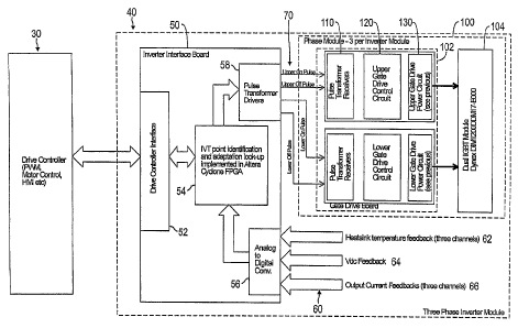
Referring to Figure 3, an embodiment of a three-phase inverter module 40
having
an adaptive gate drive according to certain teachings of the present
disclosure is
schematically illustrated. The present embodiment of inverter module 40 with
adaptive
gate drive is preferred for applications where the inverter module 40 operates
as a low
voltage control circuit that already has available signals 60 .for determining
the IVT
operating point for some or all IGBT devices in the system. Although the
inverter
module 40 is shown as being for three phases, it will be understood that the
techniques
disclosed herein may be used with inverters having different phase
configurations.
The three-phase inverter module 40 includes an inverter interface board 50 and
phase modules 100. Only one phase module 100 is shown in Figure 3 for
simplicity.
However, the three-phase inverter module 40 will have three such phase modules
100.
The inverter interface board 50 includes a drive controller interface 52, a
Field
Programmable Gate Array (FPGA) 54, analog to digital (A/D) converters 56, and
pulse
transformer drivers 58. The drive controller 30 is shown interfacing with the
drive
controller interface 52 of the inverter interface board 50. As is known in
inverter control,
the drive controller 30 sends various signals to control the inverter, such as
Pulse Width
= Modulated (PWM) signals, motor control signals, and human machine
interface (HMI)
signals. The drive controller 30 for the present embodiment can be a
conventional drive
controller used in the art of inverters. = =
The FPGA 54 communicates signals with the drive controller interface 52,
receives signals 60 from the AJD converters 56, and sends signals to the pulse
transformer drivers 58. The FPGA 54 has embedded memory for the identification
and
CA 02565453 2006-10-26
WO 2005/104743 PCT/US2005/014380
9
adaptive look-up of IVT operating points of the inverter and IGBT devices
being driven =
in the inverter. Preferably, the FPGA 54 is a CYCLONE FPGA by Altera. Although
the
present embodiment includes an FPGA, it will be appreciated that other devices
or
microprocessors known in the art can be used, such as a Digital Signal
Processing (DSP)
controller. The AID converters 56 receive analog signals 60 measured from the
inverter
circuitry and convert the signals to digital signals that are sent to the FPGA
54. The
analog signals 60 include feedback signals .62 of heatsink temperatures
measured from
the IGBT devices of the inverter circuitry. In addition, the analog signals 60
include a
=
DC voltage feedback signal 64 measured from the inverter circuitry and include
output
current feedback signals 66 measured from the output of the IGBT devices of
the inverter
circuitry.
The three-phase inverter module 40 operates six IGBT devices of the three-
phase
inverter circuitry. Thus, the AID converter 56 preferably includes a plurality
of channels
for the various feedback signals 60 for operating the six IGBT devices of the
inverter. It
will be appreciated that other inverter typologies may use other channels
connections
between the AID converter 56 and the inverter circuitry. In a preferred
embodiment,
three dual package IGBT devices 104, such as Dynex Semiconductor's
DIM1200DDM17-E000 or Eupec's FF1200R17KE3, are preferably used in the inverter
circuitry.
The FPGA 54 sends signals to the pulse transformer drivers 58, which in turn
send pulse signals to each of the phase modules 100. Each phase module 100
includes a
gate drive board 102 and a dual IGBT package 104, such as Dynex
Semiconductor's
DIM1200DDM17-E000 or Eupec's FF1200R17KE3. Each phase module 100 includes
dual arrangements of pulse transformer receivers 110, gate drive control
circuits 120, and
gate drive power circuits 130 for each of the IGBT devices of the .dual IGBT
package
104. Each phase module 100 receives four pulse signals 70 from the inverter
interface
= board 50 in the present embodiment. Two of the pulse signals 70 include
an Upper ON
pulse and an Upper OFF pulse intended for an "upper" IGBT device in the dual
IGBT
package 104 of the preferred embodiment. The other two pulse signals 70
include a
Lower. ON Pulse and a Lower OFF Pulse intended for the "lower" IGBT device in
the
dual GBT package 104 of the preferred embodiment.
CA 02565453 2006-10-26
PCT/US2005/014380
WO 2005/104743
The drive controller 30, drive controller interface 52, A/D converters 56,
pulse =
transformer drivers 58, pulse transformer receivers 110, and other components
for the
present embodiment can be conventional designs for such devices used in the
art of
power inverter circuits. The gate drive control circuits 120 and power
circuits 130,
however, are preferably similar to those disclosed below with reference to
Figure 4. As
described in more detail below, these gate drive power circuits 130 include
field-effect
transistors (FETs) for producing waveforms according to the techniques
disclosed above
with reference to Figure 2 that control the turn-off behavior of the IGBT
devices being
driven.
In operation, the FPGA 54 on the Inverter Interface Board 50 continually
monitors the temperature signals 62, the current output signals 64, and the DC
link
voltage signal 66 using the AiD converters 56. In the present embodiment, the
temperature is measured from the heatsink of the IGBT devices of the inverter
circuitry.
From the heat sink temperatures, the FPGA 54 estimates the junction
temperature for the
IGBT devices, because the junction temperature is not readily measurable in
IGBT
devices. =
The FPGA 54 estimates the junction temperature Ti using the heatsink
temperature, the current output, and the DC link voltage with the following
equation:
+K = I +K =I
hsk 1 ph 2 ph dc
Where:
Ti is the estimated junction temperature of the IGBT device,
Thsk is the heatsink temperature. feedback signal from the IGBT device,
'ph is the output current for each phase of the inverter, =
Vde is the DC link voltage feedback signal from the inverter. ,
The constants X.1 and K2 are determined experimentally based on the specific
IGBT
device and PWM frequency used in a particular implementation of the power
inverter
circuit. The equation yields an estimate of the junction temperature T.
In the preferred embodiment, the FPGA 54 reduces the resolution of the
measured
values of T, 'ph and Vdc to 4-bit resolution, which can be adequate for the
determination
of gate control adaptation according to the disclosed techniques.. The .FPGA
54 then
concatenates the 4-bit values T, 'ph and Vac to yield a 12-bit value that
represents a
CA 02565453 2006-10-26
WO 2005/104743 PCT/US2005/014380
11
current IVT operating condition for the IGBT device being driven. The FPGA 54
includes look-up tables in embedded memory for controlling the turn-off
behaviors of the
IGBT devices of the inverter circuitry according to the techniques disclosed
herein. The
look-up table includes a plurality of IVT operating points under with the
inverter is
intended to operate. Each IVT operating point has empirically derived
parameters for the
= control pulse that will best control the turn-off behavior of the IGBT
device being driven.
The parameters for the control pulse stored in the FPGA 54 include start times
(Ts) and
stop times (Tw) for the control pulses used to control the IGBT devices. The
control
pulse can have a fixed height or amplitude, which may be substantially the
same as an
ON voltage (e.g., +15V). Alternatively, the parameters in the look-up tables
of the FPGA
54 can include modified and empirically derived amplitudes for the control
pulse that will
best control the turn-off behavior of the IGBT.devices.
= During operation of the inverter, the inverter module 40 monitors the IVT
operating conditions of the inverter, and the FPGA 54 continually updates the
preferred
parameters for the control pulses that will best operate the IGBT devices of
the inverter.
As the IVT operating conditions change, the FPGA 54 looks up the preferred
parameters
(e.g., start times (Ts) and stop times (Tw)) for the control pulses that
correspond to the
current IVT operating conditions measured from the inverter and the IGBT
devices being
driven. During "turn off' of an IGBT device in the inverter, the FPGA 54 sends
command signals to the gate drive control circuit 120 for the IGBT device. At
this point,
the gate drive control circuit 120 knows the optimum start time (Ts) and stop
time (Tw)
for the control pulse that corresponds to the particular IVT operating point
of. the IGBT
device being driven. After the IGBT device begins desaturation during initial
"turn off,"
the gate drive control circuit 120 and power circuit 130 drive the IGBT device
with the
preferred control signal to control the turn-off behavior of the IGBT device
according to
the techniques 'disclosed herein. To ensure that no limit conditions exist, an
offset is
preferably used in this pulse-width encoding of the control pulse. .
=
Referring to Figure 4, embodiments of the gate drive control circuit 120 and
power circuit 130 of Figure 3 are illustrated. The gate drive control circuit
120 is
connected to the pulse transformer receivers (110 of the phase module 100 of
Figure 3) to
receive signals from the FPGA (54 of Figure 3) according to the techniques
described .
CA 02565453 2006-10-26
WO 2005/104743
PCT/US2005/014380
12
with reference to Figure 3. The gate drive power circuit 130 of Figure 4 is
connected to
the gate drive control circuit 120 and the IGBT device 20. As is known, the
collector C
and the emitter E of the IGBT device 20 are connected to the inverter
circuitry (not
shown). The gate drive control circuit 120 and power circuit 130 drive the
IGBT device
20 according to the waveform modification techniques disclosed herein.
As noted previously, a preferred embodiment of the inverter circuitry Dynex
Semiconductor's DIM1200DDM17-E000 or Eupec's FF1200R17KE3, which include
dual packaged IGBT devices. Therefore, the IGBT device 20 of Figure 4 can
represent
one of the IGBT devices in these preferred IGBT packages. Although the present
embodiment has been developed for these preferred IGBT packages, it will be
understood
that other IGBT devices known in the art can be used with the disclosed
techniques.
The gate drive power circuit 130 includes a plurality of high power field-
effect
transistors (FETs) that impose waveforms similar to those disclosed above in
Figure 2 on
the IGBT device 20. The gate drive power circuit 130 includes an ON FET 140,
an OFF
FET 150, a control FET 160,.and a desaturation detector 170. The control
circuit 120 is
electrically connected to respective gate terminals of the ON FET 140, OFF FET
150,
and control FET 160. The 'control circuit 120 sends switching control signals
to the
respective gate terminals of the FETs 140, 150, and 160 to control their
operation.
R. The source of the ON FET 140 is connected to the ON voltage,
which is typically
= +15V, while the drain of the ON FET 140 is connected to the gate G of the
IGBT device
= 20 being driven. A resistor 142 is connected between the drain of the ON
FET 140 and
the gate G of the IGBT device 20. The source of the OFF FET 150 is connected
to the
OFF voltage, which is typically +15V, while the drain of the OFF FET 150 is
also
== connected to the gate G of the IGBT device 20 being driven. A resistor
152 is connected.
= between the source of the OFF FET 150 and the gate G of the IGBT device
20. The
source of the control FET 160 is connected to a control voltage, which may be
+15V,
while the drain of the control FET 160 is connected to the gate G of the IGBT
device 20
being driven.' A diode 162 is connected between the drain .of the Control FET
160 and
= the gate G of the IGBT device 20.
The desaturation detector 170 is connected between the control circuit 120 and
the
IGBT device 20. The connection of the=desaturation detector 170 to the IGBT
device .20
=
CA 02565453 2006-10-26
WO 2005/104743 PCT/US2005/014380
13
is made between the collector C and the gate G of the IGBT device 20. The
desaturation
detector can be of conventional design and can include a reverse bias diode
and
comparator, for example. The desaturation detector 170 determines when
desaturation of
the IGBT device 20 begins after the storage time delay during initial "turn
off' of the
IGBT device 20.
The control circuit 120 operates in a typical fashion by sending control
switching
signals to the ON FET 140 and the OFF FET 150 to control the signals from
these FETs
to the gate G of the IGBT device 20 being driven. To modify the turn-off
behavior of the
IGBT device 20 to produce waveforms according to the techniques disclosed
herein, the
control circuit 120 also sends control switching signals to the gate of the
control FET 160
at a specified point during the "turn off' of the IGBT device 120. In turn,
the control
PET 160 sends a control signal of positive gate voltage as described above to
improve the
turn-off behavior of the IGBT device 20. In particular, the control FET 160
sends the
control pulse that has the optimum start time (Ts) and stop time (Tw)
determined by the
look-up table in the FPGA (54 of Figure 3) for the current TVT operating point
of the
IGBT device 20 and inverter.
In an alternative embodiment, the control circuit 120 and the power circuit
130
can modify the turn-on behavior of the IGBT device 20 according to the
techniques
disclosed herein. In addition to the ON FET 140 and resistor 142 disclosed
above, a
second ON FET (not shown) can be separately connected to the control circuit
120 and to
the gate G with a second resistor (not shown) in the same manner as the ON FET
140 and
resistor 142. The resistors 142 and (one not shown) can have different
resistances. In
this way, the control circuit 120 can send initial switching signals to the
first ON FET
140 of the ON FETs to have the corresponding resistance from its resistor 142
operate the
gate G. Then, the control circuit 120 can send subsequent switching signals to
the other
ON FET (not shown) to have the corresponding resistance from its resistor (not
shown)
operate the gate G of the IGBT device 20. The selection of the ON FETs and the
duration
of the switching signals can be determined by a look-up table in the FP.GA 54
based on
the current operating conditions of the inverter and IGBT device.
=
Referring to Figure 5, another embodiment of a gate drive control 220 and
power.
circuit 230 is illustrated. The gate drive control 220 and the power circuit
230 of the
CA 02565453 2006-10-26
WO 2005/104743 PCT/US2005/014380
14
present embodiment are preferably used in applications where the IVT operating
point of
the inverter is unknown by other components .of the inverter and control
circuitry, which
is by contrast the case with the embodiments of Figure 3 and 4. The gate drive
control =
circuit 220 is connected to signal isolation circuitry 210 and power isolation
circuitry
212. The signal isolation circuitry 210 can include pulse transformers,
optocouplers, or
other devices known in the art for isolating signals. Similarly, the power
isolation
circuity 212 can include transformers or other devices known in the art for
isolating a
control circuit from a power source. The control circuit 220 receives signals
from other
control components via the signal isolation circuitry 210. For example, the
control circuit
220 can receive Pulse Width Modulated (PWM) signals, motor control signals,
and
human machine interface (HMI) signals from a drive controller.
The gate drive power circuit 230 is connected to the gate drive control 220
and
the IGBT device 20. The gate drive power circuit 230 is used to drive the IGBT
device
20 according to the waveform modification techniques disclosed herein. As is
known,
the collector C and the emitter E of the IGBT device 20 are connected to the
inverter
circuitry (not shown). As noted previously, Dynex Semiconductor's'
DIM1200DDM17-
E000 or the Eupec's FF1200R17KE3 are used in a preferred embodiment of the
inverter
circuitry. Therefore, the IGBT device 20 of Figure 5 can represent one of the
IGBT
devices in these preferred IGBT packages. Although the present embodiment has
been
developed for these preferred IGBT packages, it will be understood that other
IGBT
devices known in the art can be used with the disclosed techniques.
Similar to the embodiment of Figure 4, the gate drive power circuit 230
includes
an ON FET 240, an OFF FET 250, a control FET 260, and a desaturation detector
270.
Further, the gate drive power circuit 230 includes a voltage divider 280, an
analog
integrator 290, and a thermistor 300. The control circuit 220 is electrically
connected to
respective gate terminals of the ON FET 240, OFF FET 250, and control FET 260.
The =
control circuit 200 sends control switching signals to the respective gate
terminals of the
FETs 240, 250, and 260 to control their operation. To overcome any practical
difficulties
. = in manufacturing, the gate drive circuit 230 is preferably implemented
on a multi-layer
printed circuit board (PCB) using modem, fine-pitch devices known in the art.
=
CA 02565453 2006-10-26
WO 2005/104743 PCT/US2005/014380
The source of the ON FET 240 is connected to the ON voltage, which is
typically
+15V, while the drain of the ON FET 240 is connected to the gate G of the IGBT
device
being driven. A resistor 242 is connected between the drain of the ON FET 240
and
the gate G of the IGBT device 20. The source of the OFF FET 250 is connected
to the
OFF voltage, which is typically +15V, while the drain of the OFF FET 250 is
also
connected to the gate G of the IGBT device 20 being driven. A resistor 252 is
connected
between the source of the OFF FET 250 and the gate G of the IGBT device 20.
The
source of the control FET 260 is connected to a control voltage, which may be
the steady-
state ON voltage (+15V), while the drain of the control FET 260 is connected
to the gate
G of the IGBT device 20 being driven. A diode 262 is connected between the
drain of
the control FET 260 and the gate G of the IGBT device 20.
The control circuit 220 receives temperature feedback of the IGBT device 20
using the thermistor 300, resistance measurement device 302, and serial .A/D
converter
304. The thermistor 300 is preferably a Negative Temperature Coefficient (NTC)
thermistor. The NTC thermistor 300 is mounted directly on the die of the IGBT
module
having the IGBT device 20. One side of the NTC thermistor 264 is connected to
the
emitter metallization of the IGBT device 20 using a metal loaded epoxy. The
other side
of the thermistor 300 is connected to the resistance measurement device 302.
The output
of the resistance measurement device 302 is connected to the serial AID
converter 304,
which sends a digital resistance signal to the control circuit 220. The
resistance of the
NTC thermistor 300 is measured during steady-state ON or OFF operation. For
example,
the resistance measurement device 302 can include a differential amplifier for
measuring
the voltage drop across the NTC thermistor 300. The voltage will be just a few
tens of
millivolts so any op-amp circuit is preferably of sufficient precision and
several
milliseconds of filtering on the input signals may be acceptable. Once the
resistance of
the NTC thermistor 300 is determined and sent to the control circuit 220 via
the serial .
AID converter 304, a look-up table inside the FPGA (not shown) of the control
circuit
220 is used to determine the temperature of the IGBT device:
The desaturation detector 270 is connected between the control circuit 220 and
the
IGBT device 200. The connection of the desaturation detector 270 to the IGBT
device 20
is made between the collector C and the gate G of the IGBT device 20. The
desaturation
CA 02565453 2006-10-26
WO 2005/104743 PCT/US2005/014380
16
detector 270 can be of conventional design and can include a reverse bias
diode and
comparator, for example. The desaturation detector 270 determines when
desaturation of
the IGBT device 20 begins after the storage time delay during initial "turn
off' of the
IGBT device 20.
The voltage divider 280 is connected between the control circuit 220 and the
IGBT device 20. The connection of the voltage divider 280 to the IGBT device
20 is also
made between the collector C and the gate G of the IGBT device 20. The
connection of
the voltage divider 280 to the control circuit 220 is made via a fast, serial
A/D converter
282. The voltage divider 280 can be of conventional design. The voltage
divider 280
measures the collector-emitter voltage VcE during the steady-state OFF
condition of the
IGBT device 20.
The analog integrator 290 has one connection connected to a freeze, reset
control
output of the control circuit 220, another connection connected to a current
feedback
input of the control circuit 220 via a fast serial A/D converter 292, and
another
connection connected to the power emitter of the IGBT module. The analog
integrator
290 can be of conventional design. The analog integrator 290 measures the
voltage
across the IGBT module's internal emitter inductance (i.e. the voltage between
the
auxiliary and power emitter terminals) during "turn on" of the device 20.
The control circuit 220 operates in typical fashion by sending control
switching
signals to the ON FET 240 and the OFF FET 250 to control the signals from
these FETs
to the gate G of the IGBT device 20 being driven. To modify the "turn off' of
the IGBT
device 20 to produce waveforms according to the techniques disclosed above,
the control
circuit 220 also sends control switching signals to the gate of the control
FET 260 at a
specified point during the "turn off' of the IGBT device 20. In turn, the
control FET 260
sends the control pulse of positive gate voltage as described above to improve
the turn-off
behavior of the IGBT device 20.
The control circuit 220 preferably includes an FPGA, which is preferably a
CYCLONE FPGA by Altera. The control circuit 220 measures the current IVT
operating
point of the IGBT device 20 and determines the optimum parameters for
controlling the
turn-off behavior of the IGBT device 20. During operation, the temperature of
the IGBT
device 20 is measured using the resistance of the NTC thermistor 302. Once the
CA 02565453 2006-10-26
WO 2005/104743 PCT/US2005/014380
17
resistance of the NTC thennistor 302 is determined, the control circuit 220
determines the
junction temperature of the IGBT device for the current IVT operating point.
The
voltage divider 280 measures the collector-emitter, voltage VcE for the
current IVT
operating point during the steady-state OFF condition. The analog integrator
290
measures. an output current for the NT operating point by integrating the
voltage across
the IGBT module's internal emitter inductance (i.e. the voltage between the
auxiliary and
power emitter terminals) during "turn on" of the device 20. The measurement of
this
output current is valid as long as the change in current during a single PWM
cycle is not
significant with respect to the modulation of the gate drive waveform. The
controller 220
continually monitors the IVT operating point of the IGBT device 20, and the
FPGA of
the controller 220 uses the NT operating point to control the gate voltage in
the same
manner as disclosed above.
Although the preferred embodiment described herein determines the
characteristics of each control pulse from predetermined values based on NT
data points,
it will be appreciated that equations, formulas or boundaries may be derived
for a specific
implementation of power semiconductors and a processor or other logic device
may
implement the equation formula or boundary to determine the control pulse
characteristic =
in real time or near real time.
The foregoing description of preferred and other embodiments is not intended
to
limit or restrict the scope or applicability of the inventive concepts
conceived of by the
Applicants. In exchange for disclosing the inventive concepts contained
herein, the
Applicants desire all patent rights afforded by the appended claims.,
Therefore, it is
intended that the appended claims include all modifications and alterations to
the full
extent that they come within the scope of the following claims or the
equivalents thereof.