Note: Descriptions are shown in the official language in which they were submitted.
CA 02565707 2012-08-20
- 1 -
LOW-HARMONICS, POLYPHASE CONVERTER CIRCUIT
Technical field
The invention relates to the field of power electronics,
and particularly to a polyphase converter circuit.
Prior art
Polyphase converter circuits are used today in a wealth of
power electronics applications. In this case, the
requirements for such a converter circuit are firstly to
produce harmonics as little as possible in an electrical AC
voltage system which is generally connected on the input
side to the converter circuit and also on phases of an
electrical load which is more conventionally connected to
the converter circuit, and secondly to transmit powers
which are as high as possible using as few electronic
components as possible. A suitable polyphase converter
circuit is specified in EP 0913 918 A2 and shown in figure
1. Therein, the converter circuit is in the form of an 18-
pulse, three-phase converter circuit and has one converter
circuit element for each phase, each converter circuit
element comprising an 18-pulse rectifier unit, a DC voltage
circuit which is connected to the rectifier unit and an
inverter unit which is connected to the DC voltage circuit.
In accordance with EP 0913 918 A2 or in accordance with
figure 1, a first AC voltage output of each inverter unit
forms a phase connection. Second AC voltage outputs of the
inverter units of the converter circuit are also star-
connected. Furthermore, the converter circuit has a single
transformer having a primary winding which is generally
connected to the electrical AC voltage system. Owing to
CA 02565707 2006-11-03
2 -
the pulse number of 18 for the converter circuit, the
transformer has nine three-phase secondary windings, in
each case three of the nine three-phase secondary
windings forming a set of secondary windings such that
in total three sets of secondary windings are formed.
GB 2 330 254 A likewise discloses a polyphase converter
circuit in which one converter circuit element is
likewise provided for each phase, each converter
circuit element having three rectifier units. A DC
voltage circuit and an inverter unit which is connected
to the DC voltage circuit are then connected to each
rectifier unit. In addition, the converter circuit from
GB 2 330 254 A has three transformers, each having a
primary winding and three three-phase secondary
windings. Furthermore, each secondary winding is
associated with one of the three converter circuit
elements, in this case each rectifier unit of the
associated converter circuit element being connected to
precisely one secondary winding associated with this
converter circuit element.
One problem with a polyphase converter circuit in
accordance with EP 0913 918 A2 is the fact that,
despite the pulse number of 18 for the rectifier units
and thus the converter circuit overall, harmonics which
are relevant on the primary winding and thus in the
electrical AC voltage system and which are greater than
the seventeenth harmonic with respect to the
fundamental of the voltage and the current of the
electrical AC voltage system may occur, and these
harmonics then place a correspondingly severe load on
the electrical AC voltage system, in particular in the
case of a weak electrical AC voltage system having a
high rated impedance. Such effects of harmonics on the
converter circuit are therefore highly undesirable.
CA 02565707 2010-01-19
3 -
Summary of the invention
it is therefore the object of the invention to specify a
polyphase converter circuit which produces harmonics which
are as low as possible with respect to the fundamental of
the voltage and the current of an electrical AC voltage
system which is connected on the input side to the
converter circuit, said converter circuit also being of
simple and robust design.
The polyphase converter circuit according to the invention
generally comprises p ? 3 output phases and a converter
circuit element provided for each phase, each converter
circuit element having a rectifier unit, a DC voltage
circuit which is connected to the rectifier unit and an
inverter unit which is connected to the DC voltage circuit.
In addition, a first AC voltage output of each inverter
unit forms a phase connection. Furthermore, second AC
voltage outputs of the inverter units are star-connected.
In accordance with the invention, n transformers are now
generally provided, each having a primary winding and m
three-phase secondary windings, where n >_ 2 and m >_ 3.
Furthermore, p sets of secondary windings are generally
provided, each set of secondary windings being formed by,
in each case, -m three-phase secondary windings of each
P
transformer, and each set of secondary windings with the
associated secondary windings being connected to the
rectifier unit of a respective converter circuit element.
Each set of secondary windings is thus associated with
only, in each case, one converter circuit element or
the rectifier unit of only, in each case, one
converter circuit element, in this case all of
the secondary windings of this set of secondary windings
CA 02565707 2006-11-03
4 -
being connected to the rectifier unit of the associated
converter circuit element. As a result of the fact that
n > 2 transformers are provided and each set of
secondary windings is formed by in each case m three-
p
phase secondary windings of each transformer, and each
set of secondary windings with the associated secondary
windings is connected to the rectifier unit of a
respective converter circuit element, the effective
pulse number of the converter circuit on the primary
side of the transformer, i.e. on the side of the
electrical AC voltage system which is connected to the
converter circuit, is greater than the pulse number of
a rectifier unit. The greater pulse number
advantageously results in essentially only very low
harmonics below the greater pulse number with respect
to the fundamental of the voltage and the current of an
electrical AC voltage system which is connected on the
input side to the converter circuit. At best, i.e.
depending on the operating state, a pulse number of 54
with respect to the fundamental of the voltage and the
current of the electrical AC voltage system results,
for example, on the primary side of the transformer in
the case of a converter circuit according to the
invention having rectifier units with a pulse number of
18, p = 3 phases and n = 3 transformers, with the
result that essentially only very low harmonics which
are lower than the fifty-third harmonic with respect to
the fundamental of the voltage and the current of the
electrical AC voltage system advantageously occur. The
electrical AC voltage system, in particular a weak
electrical AC voltage system having a high rated
impedance, is thus not loaded or is loaded to only a
small extent.
Furthermore, the converter circuit according to the
invention is of simple and robust design owing to the
abovementioned components used and their wiring.
CA 02565707 2006-11-03
-
These and other objects, advantages and features of the
present invention will become apparent from the
detailed description below of preferred embodiments of
5 the invention in conjunction with the drawing.
Brief description of the drawings
Figure 1 shows a conventional embodiment of a
polyphase, 18-pulse converter circuit,
Figure 2 shows a first embodiment of the
polyphase converter circuit according to
the invention,
Figure 3 shows a second embodiment of the
polyphase converter circuit according to
the invention,
Figure 4 shows a first embodiment of a converter
circuit element of the polyphase
converter circuit according to the
invention as shown in figure 1 or figure
2 with a first embodiment of an inverter
unit,
Figure 5 shows a second embodiment of an inverter
unit of the converter circuit element
shown in figure 4,
Figure 6 shows a frequency spectrum of an input-
side voltage of a conventional
polyphase, 12-pulse converter circuit,
Figure 7 shows a frequency spectrum of an input-
side current of a conventional
polyphase, 12-pulse converter circuit,
CA 02565707 2006-11-03
- 6 -
Figure 8 shows a frequency spectrum of an input-
side voltage of the converter circuit
according to the invention as shown in
figure 2,
Figure 9 shows a frequency spectrum of an input-
side current of the converter circuit
according to the invention as shown in
figure 2, and
Figure 10 shows a third embodiment of the
polyphase converter circuit according to
the invention.
The references used in the drawing and their
significance are listed in summary in the list of
references. In principle, the same parts are provided
with the same references in the figures. The
embodiments described represent examples of the subject
matter of the invention and have no restrictive effect.
Approaches to implementing the invention
Figure 2 shows a first embodiment of the polyphase
converter circuit according to the invention. The
converter circuit shown in figure 2 has p = 3 phases R,
Y, B, p >_ 3 phases R, Y, B generally being conceivable.
As shown in figure 2, the converter circuit comprises a
converter circuit element 1 provided for each phase R,
Y, B, each converter circuit element 1 having a
rectifier unit 2, a DC voltage circuit 3 which is
connected to the rectifier unit 2 and an inverter unit
4 which is connected to the DC voltage circuit 4. The
rectifier unit 2 shown in figure 2 has a pulse number
of x = 12, the pulse number x indicating the number of
switching pulses during one period of the voltage of an
electrical AC voltage system 11 which is connected on
the input side to the converter circuit. Furthermore, a
CA 02565707 2006-11-03
- 7 -
first AC voltage output 5 of each inverter unit 4 forms
a phase connection 6. In addition, second AC voltage
outputs 12 of the inverter units 5 shown in figure 2
are star-connected.
In accordance with the invention, n transformers 7 are
now generally provided, each having a primary winding 8
and m three-phase secondary windings 9, where n >_ 2 and
m >_ 3. As shown in figure 2, there are,.n = 2
transformers, each having m = 3 three-phase secondary
windings 9. Furthermore, p sets of secondary windings
10 are generally provided, each set of secondary
windings 10 being formed by in each case m three-phase
P
secondary windings 9 of each transformer 7, and each
set of secondary windings 10 with the associated
secondary windings 9 being connected to the rectifier
unit 2 of a respective converter circuit element 1.
Each set of secondary windings then comprises m=n
P
secondary windings 9. As is also shown in figure 2,
each set of secondary windings 10 is thus associated
with only in each case one converter circuit element 1
or the rectifier unit 2 of only in each case one
converter circuit element 1, in this case all of the
secondary windings 9 of this set of secondary windings
10 being connected to the rectifier unit 2 of the
associated converter circuit element 1. As shown in
figure 2, in the case of p = 3 phases R, Y, B, p = 3
sets of secondary windings 10 are also provided, each
set of secondary windings 10 being formed by in each
case a three-phase secondary winding 9 of each
transformer 7, and each set of secondary windings 10
comprising two secondary windings 9.
Owing to the generally n >_ 2 transformers 7 and the
fact that each set of secondary windings 10 is formed
CA 02565707 2006-11-03
8 -
by in each case m three-phase secondary windings 9 of
P
each transformer 7, and each set of secondary windings
with all of its associated secondary windings 9 is
connected to the rectifier unit 2 of a respective
5 converter circuit element 1, the effective pulse number
of the converter circuit on the primary side 8 of the
transformer 7, i.e. on the input side of the converter
circuit, is greater than the pulse number of a
rectifier unit 1. The greater pulse number
10 advantageously results in essentially only very low
harmonics below the greater pulse number with respect
to the fundamental of the voltage and the current of an
electrical AC voltage system 11 which is connected on
the input side to the converter circuit. In addition, a
frequency spectrum of an input-side voltage of a
conventional polyphase converter circuit with a pulse
number of x = 12 for the rectifier unit 2 is shown in
figure 6. The design for such a 12-pulse converter
circuit corresponds to the known converter circuit
described at the outset with a pulse number of x = 18
as shown in figure 1, in contrast to figure 1 the
conventional 12-pulse converter circuit having 12-pulse
rectifier units, and the single transformer 7 in this
case comprising six three-phase secondary windings 9,
in each case two of the six three-phase secondary
windings 9 forming a set of secondary windings 10 such
that in total three sets of secondary windings 10 are
formed. In addition, a frequency spectrum of an input-
side current of a conventional polyphase converter
circuit with a pulse number of x = 12 for the rectifier
unit 2 is shown in figure 7. In order to better
illustrate the abovementioned advantages of the greater
effective pulse number for the converter circuit
according to the invention as shown in figure 2, a
frequency spectrum of the input-side voltage of the
converter circuit according to the invention shown in
figure 2 is shown in figure 8, and a frequency spectrum
CA 02565707 2006-11-03
9 -
of the input-side current of the converter circuit
according to the invention shown in figure 2 is shown
in figure 9. At best, i.e. depending on the operating
state, a pulse number of 36 (x = p = 36) with respect to
the fundamental of the voltage and the current of the
electrical AC voltage system 11 results, for example,
on the primary side of the transformer 7 in the case of
the converter circuit according to the invention having
rectifier units 2 with a pulse number of x = 12, p = 3
phases R, Y, B and with n = 2 transformers, with the
result that essentially only very low harmonics which
are lower than the thirty-fifth harmonic with respect
to the fundamental of the voltage and the current of
the electrical AC voltage system 11 advantageously
occur. The electrical AC voltage system 11, in
particular a weak electrical AC voltage system having a
high rated impedance, is thus advantageously not loaded
or is loaded to only a small extent.
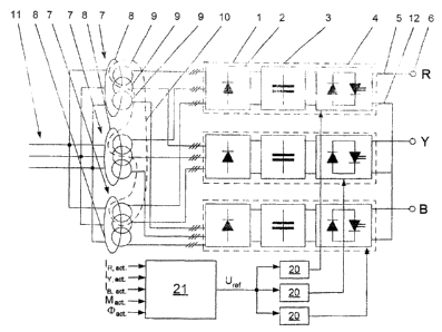
Figure 3 shows a second embodiment of the polyphase
converter circuit according to the invention. In
contrast to the first embodiment shown in figure 2, the
respective rectifier unit 2 shown in figure 3 has a
pulse number of x = 18. In addition, in contrast to the
first embodiment shown in figure 2, n = 3 transformers
are provided in the second embodiment shown in figure
3, each having m = 3 three-phase secondary windings 9.
As shown in figure 3, furthermore, in the case of p = 3
phases R, Y, B, p = 3 sets of secondary windings 10 are
also provided, each set of secondary windings 10 being
formed by in each case a three-phase secondary winding
9 of each transformer 7, and, each set of secondary
windings 10 comprising three secondary windings 9. With
the converter circuit in accordance with the second
embodiment shown in figure 3, at best, i.e. depending
on the operating state, a pulse number of 54 (x = p =
54) with respect to the fundamental of the voltage and
the current of the electrical AC voltage system 11
CA 02565707 2006-11-03
- 10 -
results, for example, on the primary side of the
transformer 7 having rectifier units 2 with a pulse
number of x = 18, p = 3 phases R, Y, B and with n = 3
transformers, with the result that essentially only
very low harmonics which are lower than the fifty-third
harmonic with respect to the fundamental of the voltage
and the current of the electrical AC voltage system 11
advantageously occur.
Figure 10 shows a third embodiment of the polyphase
converter circuit according to the invention. In
contrast to the first and second embodiments shown in
figure 2 and figure 3, the respective rectifier unit 2
shown in figure 10 has a pulse number of x = 24. In
addition, in the third embodiment shown in figure 10,
n = 2 transformers are provided, each having m = 6
three-phase secondary windings 9. As shown in figure
10, furthermore, in the case of p = 3 phases R, Y, B, p
= 3 sets of secondary windings 10 are also provided,
each set of secondary windings 10 being formed by in
each case two three-phase secondary windings 9 of each
transformer 7, and each set of secondary windings 10
comprising four secondary windings 9. With the
converter circuit in accordance with the third
embodiment shown in figure 10, at best, i.e. depending
on the operating state, a pulse number of 72 (x = p =
72) with respect to the fundamental of the voltage and
the current of the electrical AC voltage system 11
results, for example, on the primary side of the
transformer 7 having rectifier units 2 with a pulse
number of x = 24, p = 3 phases R, Y, B and with n = 2
transformers, with the result that essentially only
very low harmonics which are lower than the seventy-
first harmonic with respect to the fundamental of the
voltage and the current of the electrical AC voltage
system 11 advantageously occur.
In general and in the embodiments of the converter
CA 02565707 2006-11-03
- 11 -
circuit according to the invention shown in figure 2
and figure 3, the three-phase secondary windings 9 are
preferably phase-shifted in relation to one another
with respect to a set of secondary. windings 10. The
preferred phase shift with respect to in each case two
secondary windings 9 of a set of secondary windings 10
is an integral multiple of (60-p ) degrees. In the first
n=m
embodiment of the converter circuit according to the
invention shown in figure 2, a phase shift with respect
to in each case two secondary windings 9 of a set of
secondary windings 10 of an integral multiple of 30
degrees thus results.. Furthermore, in the second
embodiment of the converter circuit according to the
invention shown in figure 3, a phase shift with respect
to in each case two secondary windings 9 of a set of
secondary windings 10 of an integral multiple of 20
degrees results. In. addition, in the third embodiment
of the converter circuit according to the invention
shown in figure 10, a phase shift with respect to in
each case two secondary windings 9 of a set of
secondary windings 10 of an integral multiple of 15
degrees thus results. These phase shifts result at
best, i.e. depending on the operating state, in the
advantageous pulse numbers, which have already been
specified above in relation to figure 2, figure 3 and
figure 10, on the primary side of the transformer 7.
Furthermore, in general and in the embodiments of the
converter circuit according to the invention shown in
figure 2, figure 3 and figure 10, the three-phase
secondary windings 9 are phase-shifted in relation to
one another with respect to a transformer 7. The
preferred phase shift with respect to in each case two
secondary windings 9 of a transformer 7 is an integral
multiple of (60 ) degrees or (360) degrees, where x is
n=m x=p
the abovementioned pulse number of a rectifier unit 2.
CA 02565707 2006-11-03
- 12 -
The formulae specified above for the phase shift with
respect to in each case two secondary windings 9 of a
transformer 7 are equivalent. In the first embodiment
of the converter circuit according to the invention
shown in figure 2, a phase shift with respect to in
each case two secondary windings 9 of a transformer 7
of an integral multiple of 10 degrees thus results.
Furthermore, in the second embodiment of the converter
circuit according to the invention shown in figure 3, a
phase shift with respect to in each case two secondary
windings 9 of a transformer 7 of an integral multiple
of 6 2/3 degrees results. Furthermore, in the third
embodiment of the converter circuit according to the
invention shown- in figure 10, a phase shift with
respect to in each case two secondary windings 9 of a
transformer 7 of an integral multiple of 5 degrees
results. This phase shift advantageously results in
secondary-side elimination of harmonics with respect to
the fundamental of the voltage and the current of an
electrical AC voltage system which is connected on the
input side to the converter circuit.
Furthermore, in general and in the embodiments of the
converter circuit according to the invention shown in
figure 2, figure 3 and figure 10, the primary windings
8 of the transformers are phase-shifted in relation to
one another. The preferred phase shift with respect to
in each case two primary windings is an integral
multiple of 60/n degrees. In the first embodiment of
the converter circuit according to the invention shown
in figure 2 and in the third embodiment shown in figure
10, a phase shift with respect to in each case two
primary windings 8 of an integral multiple of 30
degrees thus results. Furthermore, in the second
embodiment of the converter circuit according to the
invention shown in figure 3, a phase shift with respect
to in each case two primary windings 8 of an integral
multiple of 20 degrees results. This above-described
CA 02565707 2006-11-03
- 13 -
phase shift of the primary windings 8 with respect to
in each case two transformers 7 results in an identical
arrangement design for the secondary windings 9 of the
transformer 7, with the result that production can be
simplified and thus, in addition, costs can be saved.
Figure 4 illustrates a first embodiment of a converter
circuit element 1 of the polyphase converter circuit
according to the invention shown in figure 1 or figure
2 with a first embodiment of an inverter unit 4. The
converter circuit element 1 comprises the
abovementioned DC voltage circuit 3, which is formed by
two series-connected capacitors and has a first main
connection 14, a second main connection 15 and a
connection element 16 formed by the two adjacent
capacitors which are connected to one another. As shown
in figure 4, the inverter unit 4 has two pairs of
branches 13 for the purpose of connecting three
switching voltage levels, the respective pair of
branches 13 having a first, second, third and fourth
drivable, bidirectional power semiconductor switch S1,
S2, S3, S4 and a fifth and sixth power semiconductor
switch S5, S6. Each drivable, bidirectional power
semiconductor switch Si, S2, S3, S4 is in particular
formed by a hard-switched gate turn-off thyristor or by
an insulated gate bipolar transistor (IGBT) and by a
diode which is connected back-to-back in parallel with
the gate turn-off thyristor or bipolar transistor.
However, it is also conceivable for an abovementioned
drivable, bidirectional power semiconductor switch to
be in the form of, for example, a power MOSFET having a
diode which is also connected back-to-back in parallel.
As shown in figure 4, the fifth and sixth power
semiconductor switches S5, S6 are non-drivable,
unidirectional power semiconductor switches, each
formed by a diode. In this case, the fifth and sixth
power semiconductor switches form a passive clamping
switching group. As shown in figure 4, in the case of
CA 02565707 2006-11-03
- 14 -
each pair of branches 13 the first, second, third and
fourth power semiconductor switches Sl, S2, S3, S4 are
connected in series and the first power semiconductor
switch Sl is connected to the first main connection 14,
and the fourth power semiconductor switch S4 is
connected to the second main connection 15.
Furthermore, the fifth and sixth power semiconductor
switches S5, S6 are connected in series, the connecting
point between the fifth power semiconductor switch S5
and the sixth power semiconductor switch S6 being
connected to the connection element 16, the fifth power
semiconductor switch S6 being connected to the
connecting point between the first power semiconductor
switch Si and the second power semiconductor switch S2,
and the sixth power semiconductor switch S6 being
connected to the connecting point between the third
power semiconductor switch S3 and the fourth power
semiconductor switch S4. Figure 5 shows a second
embodiment of an inverter unit 4 of the converter
circuit element 1 shown in figure 4. In contrast to the
first embodiment of the inverter unit 4 shown in figure
4, in the second embodiment of the inverter unit 4
shown in figure 5 the fifth and sixth power
semiconductor switches S5, S6 are likewise drivable,
bidirectional power semiconductor switches. Each
drivable, bidirectional power semiconductor switch S5,
S6 is in particular formed by a hard-switched gate
turn-off. thyristor or by an insulated gate bipolar
transistor (IGBT) and by a diode which is connected
back-to-back in parallel with the gate turn-off
thyristor or bipolar transistor. However, it is also
conceivable for an abovementioned drivable,
bidirectional power semiconductor switch to be in the
form of, for example, a power MOSFET also having a
diode connected back-to-back in parallel. As shown in
figure 5, the fifth and sixth power semiconductor
switches S5, S6 then form an active clamping switching
group.
CA 02565707 2006-11-03
- 15 -
The DC voltage circuit 3 shown in figure 4 preferably
has a resonant circuit 17 which is tuned to a harmonic
frequency. The resonant circuit 17 comprises an
inductance and a capacitance which is connected in
series with said inductance, the resonant circuit 17
being connected in parallel with the two series-
connected capacitors in the DC voltage circuit 3. It is
advantageously possible, owing to the resonant circuit
17, for a lower-order harmonic occurring in the DC
voltage of the DC voltage circuit 3, for example, with
respect to the fundamental of the voltage of the
electrical AC voltage system 11, such as the second
harmonic, to be filtered out by corresponding tuning.
Furthermore, a smoothing inductance 18 is connected
between the rectifier unit 2 and the DC voltage circuit
3, as shown in figure 4. This smoothing inductance 18
advantageously serves the purpose of smoothing the
direct current in the DC voltage intermediate circuit 3.
Furthermore, as shown in figure 4, a current rise limit
circuit 19 is preferably connected between the DC
voltage circuit 3 and the inverter unit 4, said current
rise limit circuit 19 being connected in particular to
the first main connection 14, to the second main
connection 15 and to the connection element 16 in the
DC voltage circuit 3, in this case the two pairs of
branches 13 being connected to the current rise limit
circuit 19, as shown in figure 4. It is advantageously
possible by means of the current rise limit circuit 19
for rates of current rise to be limited which are
produced in the event of switching procedures of the
power semiconductor switches Si, S2, S3, S4, S5, S6 and
lie above the maximum permissible value for the power
semiconductor switches Si, S2, S3, S4, S5, S6.
It goes without saying that the converter circuit
element 1 shown in figure 4 having the above-described
CA 02565707 2006-11-03
- 16 -
components 17, 18, 19 may also be configured using the
second embodiment of the inverter unit 4 shown in
figure 5.
In contrast to the converter circuit element 1 shown in
figure 4, it is also conceivable for the DC voltage
circuit 3 to be formed only by one capacitor, the DC
voltage circuit 3 in this case only having a first and
second main connection 14, 15 but no connection element
16. The inverter unit 4 in this case has two pairs of
branches for the purpose of connecting two switching
voltage levels, the pairs of branches being connected
to the first and second main connections 14, 15. It
goes without saying that such a converter circuit
element 1 may likewise be provided with the components
17, 18, 19 which have been described and are shown in
figure 4.
In the converter circuit according to the invention
shown in figure 3, each inverter unit 4 has an
associated local controller unit 20, drivable power
semiconductor switches Si, S2, S3, S4, S5, S6 of the
inverter unit 4 being connected to the associated local
controller unit 20. Furthermore, a higher-order
controller unit 21 is provided which is connected to
each local controller unit 20. The higher-order
controller unit 21 shown in figure 3 is preferably fed,
on the input side, each phase connection current actual
value IR,act. r IY,act. r IB,act. of each phase connection 6,
the torque actual value Mact. and the magnetic flux
actual value (Dact. of a rotating electrical machine
which can be connected to the phase connections 5. The
torque actual value Mast. and the magnetic flux actual
value (Dact. are observed by a separate observer, which
is not illustrated in figure 3 for reasons of clarity,
from the phase connection current actual values IR,act.
IY,act.r IB,act. and the phase connection voltage actual
values. In addition, a voltage reference value Uref is
CA 02565707 2006-11-03
- 17 -
present at the output of the higher-order controller
unit 21 and is fed to each local controller unit 20 on
the input side. The higher-order controller unit 21
advantageously serves the purpose of observing the
variables of the electrical machine such as torque
actual value Mact. and magnetic flux actual value (Dact.
The higher-order controller unit 21 serves the purpose
of regulating the torque and is used for system control
of the entire converter circuit. The local controller
units 20 advantageously serve the purpose of regulating
the potential of the center point of the DC voltage
circuit 3 of the respective converter circuit element.
Then,. corresponding switching signals are produced from
the voltage reference value Uref for the purpose of
driving the drivable power semiconductor switches Sl,
S2, S3, S4, S5, S6 of the associated inverter unit 4
such that the phase voltage which is present at the
respective phase connection 6 corresponds to the
associated voltage reference value Uref in the regulated
state. This distributed structure of local controller
units 20. and a higher-order controller unit 21 reduces
the number of connections required within the entire
converter circuit and makes it possible for phase-
related control tasks to be carried out locally on the
drivable power semiconductor switches Si, S2, S3, S4,
S5, S6.
CA 02565707 2006-11-03
- 18 -
List of references
1 Converter circuit element
2 Rectifier unit
3 DC voltage circuit
4 Inverter unit
First AC voltage output
6 Phase connection
7 Transformer
8 Primary winding
9 Secondary winding
Set of secondary windings
11 Electrical AC voltage system
12 Second AC voltage output
13 Pair of branches
14 First main connection of the DC voltage circuit
Second main connection of the DC voltage circuit
16 Connection element of the DC voltage circuit
17 Resonant circuit
18 Smoothing inductance
19 Current rise limit circuit
Local controller unit
21 Higher-order controller unit