Note: Descriptions are shown in the official language in which they were submitted.
CA 02565752 2006-10-26
MEMS Sensor Systems and Methods
SACKGROUND
Fabrication of micro electro-meehanical systems (MEMS) is being refined every
day,
creating a multitude of single-axis sensors. Multi-axis sensors are cuurrently
production limited to
2-axis with the optimal 3-axis design efficientiy unattainable for measuring 6
degrees of freedom
(6-DOF). Although inertial measurement units (Il-q'tJs) are available that
provide 6-DOF
capability, they are composed of multiple individual sensors assembled in a 3-
axis triad.
Inherently, misalignment errors result from even minor imperfections during
this assembly
process. Additionally, as IMtJs today are constructed from multiple individual
accelerometers
and gyros, their implementation methods are more expeasive and error prone.
For the reasons stated above and i'or other reasons stated below which will
become
apparent to those skilled in the art upon reading and understanding the
specification, thex+e is a
need in the art for techniques of reducing misalignment errors in micro
electzvi-nnechanical
systems.
SUMM,AYtY
The Embodiments of the present invention provide methods and systems for 3-
axis
M1TMS sensor systems and methods and will be understood by reading and
studying the
following specil'wation.
In one embodiment, a six degree of freedom inertial sensor is provided. The
sensor
comprises a first silicon wafer segment having at least oue inertial sensor
pair, a second silicon
wafer scgment having at least one inertial sensor; wherein the at least one
inertial sensor pair
comprises one or both of an accelerometer pair and a gyroscope pair; wherein
the at least one
inertial sensor comprises one or both of an accelerometer and a gyroscope; and
wherein the first
silicon wafer segment and the second silicon wafer segment are bonded together
such the at least
one inertial sensor pair and the at least one inertial sensor are orientated
orthogonal to each other.
In another embodiment, a method for producing a six degree of freedom inertial
sensor is
provided. The method comprises fabzicating a first silicon wafer segment
having at least one
inertial sensor pair, whercin the at least one inertial sensor pair comprises
one or both of a pair of
orthogonally oriented accelerometers and a pair of orthogonally oriented
gyroscopes; fabricating
a second silicon wafer segment having at least one inertial sensor, wherein
the at least one
CA 02565752 2006-10-26
HONEYWELL DOCKET H0009650-5801 2
inertial sensor comprises one or both of an accelerometer and a gyroscope;
assembling together
the first silicon wafer segment and the second silicon wafer segment, wherein
the first silicon
wafier segment and the second silicon wafer are assembled together such that
the at ]east one
inertial sensor pair and the at least ono inertial sensor are oriented
orthogonal to each other; and
bonding the first silicon wafer segment to the second silicon wafer segment.
In yet another embodiment, a six degree of fresdoin inertial sensor is
provided. The
sensor compris" means for detecting one or both of acceleration and motion in
a direction of a
first axis; means for detecting one or both of acceleration and motion in a
direction of a second
access orthogonal with the first axis; means for deteeting one or both of
acceleration and motion
in a direction of a third axis orthogonal with the first axis and the second
axis; wherein the means
for detecting one or both of acceleration and motion in a direction of a
fi'rSt axis and the means
for detecting one or both of acceleration and motion in a direction of a
second access are located
on a Srst silicon wafer means and the means for detecting one or both of
acceleration and motion
in a direction of a third axis is located on a second silicon wafer means; and
means for bonding
the first silicon wafer means to ft second silicon wafer means.
DRAWINGS
Embodiments of the present invention can be rnore easily understood and
further
advantages and uses theraof more readily apparent, when considered in view of
the description
of the prefernd embodiments and the fnllowing figures in which:
Figures 1 A and 1 B are illustrations of one ombodiment of an inertial sensor.
Figure 2 is an illustration of one embodiment of production of a first silicon
wafer
segment.
Figure 3 is a flow chart of one embodiment of a method for producing a fust
silicon
wafer segment.
Figure 4 is an illustration of one embodiment of production of a second
silicon wafer
segment of one embodiment of the present invention.
Figure 5 is a flow chart of one embodiment of a method for producing a secrnid
silicon
wafer segment.
CA 02565752 2006-10-26
HONEYWELL DOCKET H0009650-5801 3
Figure 6 is a flow chart of one embodiment of a method for producing a six
degree of
froedom inertial sensor from a first silicon wafer segmeatt and a second
silicon wafe; segment.
In accordance with common practice, the various described features are not
drawn to
scale but are drawn to emphasize features relevant to the present invention.
Referem characbers
denote like elements throughout ftgures and text.
DETAILED DESCRIPTYON
In the following detailed description, referance is made to the accompanying
drawings
that form a part hereof, and in which is shown by way of specific itWstrative
embodiments in
which the invention may be practiced. These etrabodiments are described in
sufficient detail to
enable those skilled in the att to practice the invention, and it is to be
understood that other
embodiments may be utilized and that logical, mechanical and olectrical
changes may be made
without departing from the scope of the presont invention. The following
detailed descxiption is,
therefore, not to be taken in a limiting sense.
Embodiments of the present invention provide system and methods to reduce
misalignment errors, as well as the cost of producing MEMS inertial ser+,SOrs
for use in
applications such as, but not limited to, commercial, military and space
applications.
Embodiments of the present invention exploit the benefits of producing
multiple sensors on
silicon wafers, using extremely accurate, and cutrently available integrated
circuit and MEMS
fabrication methods. By producing multiple sensors on a chip, the cost of
development is vastly
reduced, perrnitting the use of this technology in broad markets. Because
fabrication methods
presented by embodiments of the present invention are very precise, a
reduction in sensor error
cross-coupling and misalignment is achieved. The resulting improvements in
overall IMU
sensor performance results in both cheaper and more accurate 6-DOF sensors.
Embodiments of the present invention utilize current accelerometer and
gyroscope
designs in a homogeneous micro-fabricadon process to fabricate both
accelerometers and
gyrmscopes on the same silicon wafers. After fabricating both accelerometers
and gyroscopes on
two single wafers, embodiments of the present invention provide methods to cut
and bond the
two wafers to generate a third sensor axis for an all attitude inertial
navigation solution. The
result is a single 6-DpF MEMS sensor that is both cheaper and tnore accurate
than 6-DpF
sensoxs available in the art today.
CA 02565752 2006-10-26
HONEYWELL DOCKET tt00o9650-5$Ol 4
Figures lA and 1B itlustrdte a 6-DOF MEMS sensor 100 of one einbodirment of
the
present invention. Sensor 100 comprises a first wafer segrnent 110 having two
accelerotneters
120-i and 120-2 oriented to ttlBaSUre accelerations on axes perpelldictilar
with resp6Gt to each
other, and two gymscopes 125-1 and 125-2 oriented to measure motion on axes
perpendicular
with respect to each other. Sensor 100 further comprises a second wafer
segment 115
assembled into a perpendicular orientation with first wafer segment 110. In
one embodiment,
first wafer segment 110 includes amounting trench 116 into which second wafer
segment 115 is
vertically inserted, as illustrated in Figure IB. In one embodiment, first
wafer segment I 10 and
second wafer segment 115 are bonded together using a silicon fusion bonding or
similar process.
Second wafer segment 115 includes an accelerometer 120-3 oriented to measure
accelerations on
an axis perpendicular with respect to accelerometess 120-1 and 120-2, and a
gyroscope 125-3
oriented to measure motion on an axis that is orthogonal with respect to
gyroscopes 125-1 and
125-2. In one embodiment, first and second wafer segments 110 and 115,
respectively azm
electrically coupled together via contact bridges 127-1 and 127-2. The
resultant 6-DOF MEMS
sensor 100 is a set of inertial sensors comprising of mutually orthogonal
accelerometers, 120-1,
120-2,120-3 and mutually orthogonal gyroscopes 125-1, 125-2 and 125-3. 6-
DOFMEMS
sensor 100 is thus installable as a single sensor device package rather than
as a triad of single
axis sensors individuaIIy packaged and mounted. One advantage of sensor 100 is
that the axes of
accelerometers, 120-1 to 120-3 and gyroscopes 125-1 to 125-3 are inhEnrntly
aligned with
respect to each other to a high degree of precision afforded by integrated
circuit manufacturing
processes. In conixast, triads of single axis sensors typically comprise
single axis sensors
mechanically -nounted orthogonally on a separate bracket or housing, with the
limited alignment
precision inherent in sueii mechanical mountings. In addition, sensor 100 is
effectively immune
to internal alignment shifts due to thermal effects and ageing, unlike
mechanically mounted
single axis sEnSor triads.
One skilled in the art would recognize that wafer segments, such as wafer
segments 110
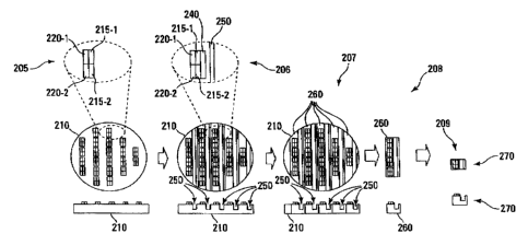
and 115 are typicaIly produced in bulk from larger silicon wafers. Figures 2
and 3 illustrate one
method for producing a wafer segment 110 of one embodiment of the present
invention from
such a larger silicon wafer 210. Shown generally at 205 in Figure 2, in one
embodiment, silicon
wafer 210 comprises a plurality of accalerometer pairs 215-1 and 215-2 and
l;ycoscope pairs 220-
1 and 220-2 oriented as described with respect to wafer segment 110 of Figure
1. As would be
appreciated by one alrilled in the art upon reading this specification, there
are any number of
ways of fabricating silicon wafer 2 I0, as discussed in more detail below.
Figure 3 is a flow chart
CA 02565752 2006-10-26
HONEY WSLL DOCKET Ei000965e-5801 5
illustrating a method for fabrieating a first silicon wafGr segment 110 from
silicon wafer 210, of
one embodiment of the pnsent invention. The method begins at 310 with applying
one or more
contact bridges 240 (shown generally in Figure 2 at 206). In one embodiment,
contact bridges
240 comprise gold (Au) electroplating, or other similar electrical conducting
material. In one
embodiment, one or more contact bridges 240 are applied for each of
accelerometers pairs 215
and gyroscope pairs 220. In one embodiment, applying contact bridges 240
comprises applying
phosphorus-doped silicon dioxide (PSG) photoresist material deposited with a
chemical-vapor
deposition (CVD) and masldng with lithography etching and sputter deposition.
In ot-e
embodiment, the method proceeds at 320 with etching one or more mounting
trenches 250
(shown generally in Figure 2 at 206). In one embodiment, etching one or more
mounting
trenches 250 comprises masking with lithography and deep reactive ion etching
(DRIE). In one
embodiment, the photrntsist is removed using a hydrofluorie-acid (HF) etch
followed by one or
more de-ionized water soaks. In one embodiment, the method continues at 330
with cutting and
separating wafer 210 into cross sections 260 (shown generally in Figure 2 at
207 and 208)
parallel to contact bridges 240, In one embodiment, the method proceeds to 340
with cutting and
separating cross sections 260 into individual wafer segments 270 (shown
gonerally in Figuti+e 2 at
209).
Figares 4 and 5 illustrate one method for produciztg a second wafer segment
115 of one
embodiment of the present invention from a larger silicon wafer 410. Showu
generally at 405 in
Figure 4 in one embodiment, a silicon wafer 410 comprises a plurality of
single axis
accelerometers 415 and gyroscopes 420 as described with respect to wafer
segment 115 of
Figure I. Figure 5 is a flow chart illustzgting a method for fabricating a
second silicon wafer
segment 115 from silicon wafer 410, of one embodiment of the preseat
invention. The method
begins at 510 with applying one or more contact bnridges 440 (shown generaliy
in Figure 4 at
406). In one embodiment, contact bridges 440 comprise Au electroplating, or
other sinrlilar
electrical conducting material. In one embodiment, one or more Au
eleceroplating contact
bridges is applied for each accelerometer 415 and gyroscope 420. In one
embodiment, applying
contact bridges 440 is comprised of applying PSG photoresist with a CVD and
masking with
lithography etching and sputter deposition. In one embodiment, the photoresist
is removed using
an HF etch followed by one or more de-ionized water soaks.. In one embodiment,
the method
continues at $20 with cutting and separating wafer 410 into cross sections 460
(shown generally
in Figure 4 at 407 and 408) parallel to contact bridges 440. ln one
embodiment, the method
CA 02565752 2006-10-26
HONEYWELL DOCKET H0009650-5801 6
proceeds to 530 with cutting and separating cross sections 460 into individual
wafer segments
470 (shown generdlly in Figure 4 at 409).
A complete 6-DOF MEMS sensor, such as sensor 100, is produced from wafer
segments
270 and 470 as illustrated by the method presented by Figure 6. In one
embodiment, the method
begins at 610 with assembling wafcr segment 470 and wafer segment 270 into a
single sensor as
portrayed in Figure ]8. In one embodiment, assembling the wafer segments is
comprised of
inserting wafer segment 470 vertically into mounting trench 250 of wafer
segment 270 such that
contact bridge 240 contacts contact bridge 440 and accelerometer pairs 215 and
gyroscope pairs
220 are orthogonal in axis with accelerometer 415 and gyroscope 420,
respectively. The method
then proceeds to 620 with bonding wafer segenent 270 to wafer segment 470. In
one
embodiment, wafer segn-ent 270 and wafer segment 470 are bonded.together using
a process
such as, but not limited to, silicon fusion bonding.
Although this specification provides illustrative deseriptions of a 6-DOF MEMS
sensor
having two accelerometers and two gyroscopes on one wafer segment, and one
acceletnmeter
and one gyroscope on the other, embodiments of the present invention are not
so limited. To the
eonttary, embodiments of the present invention include wafer segments
comprising any number
of iutertial sensors so long as the 6-DOF MEMS sensor comprises at least three
orthogonally
oriented sensors. For example, in an alternate embodiment a first wafer
segment comprises four
gyroscopes and two accelerometers and the second wafer segcnent comprises two
gyroscopes and
four accelerometers, so long as at least three of the aCCelerometers or at
least three of the
glrtoscopes are orthogonally oriented with respect to each other.
As would be appreciated by one skilled in the art upon reading this
specification, there
exist a number of techniques available for fabricating inertial sensors such
as accelerometers
120-1 to 120-3 and gyroscopes 125-1 to 125-3 in wafer segments ] 10 and 115 of
Figure IA. For
example, in one embodirnent, accelerometers 120-1 to 120-3 are fabricated in
wafer segrnents
110 and 115 using the Honeywell, Inc. capacitive pendulous accelerometer
design and HIMEMS
process. As another example, in one e2nbodiment, gyroscopes 125-1 to 125-3 are
fabricated onto
wafer segments I 10 and 115 using the vibratory-rate gyroscope designed by
Morgan Research
Corp. in conjunction with the U.S. Airny Aviation and Missile Command and The
Aegis
Technologies Group. As would be appreciated by one skilled in the art upon
reading this
specification, thesc accelerometer and gyroscope designs are compatible with
each other such
CA 02565752 2006-10-26
HONEYWELL DOCKET H0009650-5801 7
that they can be manufactured in the same process in order to fabricate them
on the same silicon
wafer.
Although specific embodiments have been illustrated and described herein, it
will be
appneciated by those of ordinary skill in the art that any azrangement, which
is calculated to
achieve the same purpose, may be substituted for the specific embodiment
showa. This
application is intended to cover any adaptations or variations of the present
inventiori. Therefore,
it is manifestly intez-ded that this invention be limited only by the claims
and the equivalents
thereof.