Note: Descriptions are shown in the official language in which they were submitted.
CA 02565765 2006-11-03
WO 2005/114282 PCT/US2005/017029
NANOWIRES AND NANORIBBONS AS SUBWAVELENGTH OPTICAL
WAVEGUIDES AND THEIR USE AS COMPONENTS
IN PHOTONIC CIRCUITS AND DEVICES
CROSS-REFERENCE TO RELATED APPLICATIONS
[0001] This application claims priority from U.S. provisional application
serial
number 60/571,416 filed on May 13, 2004, incorporated herein by reference in
its entirety, and from U.S. provisional application serial number 60/643,612
filed on January 12, 2005, incorporated herein by reference in its entirety.
STATEMENT REGARDING FEDERALLY SPONSORED RESEARCH
OR DEVELOPMENT
[0002] This invention was made with Government support under Contract No.
DE-FG02-02ER-46021 awarded by the Department of Energy and Contract
No. DMR-0092086 awarded by the National Science Foundation. The
Government has certain rights in this invention.
INCORPORATION-BY-REFERENCE OF MATERIAL
SUBMITTED ON A COMPACT DISC
[0003] Not Applicable
NOTICE OF MATERIAL SUBJECT TO COPYRIGHT PROTECTION
[0004] A portion of the material in this patent document is subject to
copyright
protection under the copyright laws of the United States and of other
countries. The owner of the copyright rights has no objection to the facsimile
reproduction by anyone of the patent document or the patent disclosure, as it
appears in the United States Patent and Trademark Office publicly available
file or records, but otherwise reserves all copyright rights whatsoever. The
copyright owner does not hereby waive any of its rights to have this patent
document maintained in secrecy, including without limitation its rights
pursuant
to 37 C.F.R. 1.14.
-1-
CA 02565765 2006-11-03
WO 2005/114282 PCT/US2005/017029
BACKGROUND OF THE INVENTION
1. Field of the Invention
[0005] This invention pertains generally to optical waveguides, and more
particularly to nanoribbons and nanowires employed as subwavelength optical
waveguides as well as optical probes, sensors, routers and other devices
based on nanoribbon/wire optical waveguides.
2. Description of Related Art
[0006] Chemically synthesized nanowires represent a unique class of building
blocks for the construction of nanoscale electronic and optoelectronic
devices.
Since nanowire synthesis and device assembly are typically separate
processes, nanowires permit more flexibility in the heterogeneous integration
of different materials than standard silicon technology allows, although the
assembly itself remains a major challenge. The toolbox of nanowire device
elements is growing and currently includes various types of transistors, light
emitting diodes, lasers, and photodetectors. While the electrical integration
of
simple nanowire circuits using lithography has been demonstrated, optical
integration, which promises higher speeds and greater device versatility,
remains unexplored.
[0007] Photonics, the optical analogue of electronics, shares the logic of
miniaturization that drives research in semiconductor and communications
technology. The ability to manipulate pulses of light within sub-micron spaces
is vital for highly integrated light-based devices, such as optical computers,
to
be realized. Recent advances in using photonic bandgap and plasmonic
phenomena to control the flow of light are impressive in this regard. However,
both of these approaches typically rely on difficult and costly lithographic
processes for device fabrication and are in early stages of understanding and
development.
BRIEF SUMMARY OF THE INVENTION
[0008] A potentially simpler and equally versatile concept is to assemble
photonic circuits from a collection of nanoribbon/nanowire elements that
assume different functions, such as light creation, routing and detection.
Accordingly, the present invention generally comprises a subwavelength
-2-
CA 02565765 2006-11-03
WO 2005/114282 PCT/US2005/017029
optical waveguide formed from a nanoribbon or nanowire having a diameter
that is less than the wavelength of light to be guided. Such a subwavelength
waveguide can serve a fundamental element of photonic circuits of various
types.
[0009] Chemically synthesized nanoribbons and nanowires have several
features that make them good building blocks, including inherent one-
dimensionality, a variety of optical and electrical properties, good size
control,
low surface roughness and, in principle, the ability to operate both above and
below the diffraction limit. An important step toward integrated
nanoribbon/wire photonics is to develop a nanoribbon/wire waveguide that can
couple pairs of nanoribbon/wire elements and provide the flexibility in
interconnection patterns that is needed to carry out complex tasks, such as.
logic operations.
[0010] Accordingly, one aspect of the invention is the assembly of photonic
circuit elements from nanostructures such as Sn02 nanoribbon and ZnO
nanowire waveguides. In one embodiment, high aspect ratio (e.g., >1000)
nanoribbons/nanowires with diameters below the wavelength of light (typically
100 nm to 400 nm) are used as waveguides of both their own internally
generated photoluminescence (PL) and nonresonant UV/visible light emitted
from adjacent, evanescently coupled, nanoribbons/wires or external laser
diodes
[0011] According to another aspect of the invention, the length, flexibility
and
strength of these single-crystalline structures enable them to be manipulated
and positioned on surfaces to create various single-ribbon shapes and multi-
ribbon optical networks, including ring-shaped directional couplers and
nanoribbon/wire emitter-waveguide-detector junctions.
[0012] Another aspect of the invention is that the ability to manipulate the
shape of active and passive nanoribbon/wire cavities provides a new tool for
investigating the cavity dynamics of subwavelength structures. Moreover,
future advances in assembling the diverse set of existing nanowire building
blocks could lead to a novel and versatile photonic circuitry.
[0013] Another aspect of the invention is that nanoribbons/nanowires push
-3-
CA 02565765 2006-11-03
WO 2005/114282 PCT/US2005/017029
subwavelength optical fibers beyond silica. The scores of materials that can
be made in nanoribbon/wire form include active, passive, nonlinear and
semiconducting inorganic crystals, as well as a wide variety of polymers.
Simultaneous photon, charge carrier and spin manipulation is possible within
and between nanowires of different compositions. Also, many of these
materials have higher refractive indices than silica-based glasses, permitting
light of a given wavelength to be confined within thinner structures for
denser
integration.
[0014] Another aspect of the invention is waveguiding in liquids using
subwavelength nanoribbon/wire optical waveguides.
[0015] According to another aspect of the invention, nanoribbons/wires are
freestanding, mechanically flexible elements that can be manipulated on
surfaces or used as mobile probes in fluids. As such, they offer a type of
versatility difficult to achieve with lithographically-defined structures that
are
permanently affixed to their substrates.
[0016] Another aspect of the invention is a nanoribbon/wire optical waveguide
having a high aspect ratio and a diameter less than the wavelength of light to
be guided. In one embodiment, the aspect ratio is greater than approximately
1000. In another embodiment, the diameter is in the range of approximately
100 nm to approximately 400 nm.
[0017] Another aspect of the invention is a subwavelength optical waveguide
formed from a crystalline oxide nanoribbon/wire. In one embodiment, the
nanoribbon/wire comprises Sn02. In another embodiment, the
nanoribbon/wire comprises ZnO. In still another embodiment, the
nanoribbon/wire comprises GaN.
[0018] Another aspect of the invention is to provide a nanoribbon/wire laser
and a nanoribbon/wire photodetector coupled by a nanoribbon/wire optical
channel.
[0019] Another aspect of the invention is an optical waveguide comprising a
nanoribbon/wire dispersed on an Si02 or mica substrate.
[0020] Another aspect of the invention is a method of forming a Sn02
nanoribbon/wire waveguide.
-4-
CA 02565765 2006-11-03
WO 2005/114282 PCT/US2005/017029
[0021] Another aspect of the invention is a method of forming a ZnO
nanoribbon/wire waveguide.
[0022] A further aspect of the invention is an apparatus for guiding light
through liquid media, comprising a nanoribbon or nanowire waveguide. In one
embodiment, the nanoribbon waveguide comprises a Sn02 nanoribbon
waveguide. In another embodiment, the nanowire waveguide comprises a
ZnO nanowire waveguide. In a further embodiment, the waveguides comprise
high dielectric waveguides. In still another embodiment, the nanowire
waveguide comprises a GaN nanowire waveguide.
[0023] Another aspect of the invention is a probe or a sensor comprising a
subwavelength nanostructure waveguide.
[0024] A further aspect of the invention is an optical router comprising at
least
two coupled nanoribbon waveguides. In one embodiment, the nanoribbon
waveguides comprise Sn02 nanoribbon waveguides.
[0025] Another aspect of the invention is an optical router comprising at
least
two coupled nanowire waveguides. In one embodiment, the nanowire
waveguides comprise ZnO nanowire waveguides.
[0026] Still another aspect of the invention is an optical router comprising a
network of nanoribbon waveguides configured to separate white light and
route individual colors based on a short-pass filtering effect. In one
embodiment, the nanoribbon waveguides comprise Sn02 nanoribbon
waveguides.
[0027] Another aspect of the invention is an optical crossbar grid comprising
two pairs of orthogonal nanoribbon waveguides configured to conduct light
through abrupt 90 angles. In one embodiment, the nanoribbon waveguides
comprise Sn02 nanoribbon waveguides.
[0028] Further aspects of the invention will be brought out in the following
portions of the specification, wherein the detailed description is for the
purpose of fully disclosing preferred embodiments of the invention without
placing limitations thereon.
-5-
CA 02565765 2006-11-03
WO 2005/114282 PCT/US2005/017029
BRIEF DESCRIPTION OF THE SEVERAL VIEWS
OF THE DRAWING(S)
[0029] The invention will be more fully understood by reference to the
following drawings which are for illustrative purposes only:
[0030] FIG. 1A-C illustrate optical waveguiding in a 715 pm long SnO2
nanoribbon.
[0031] FIG. 2A-F illustrate panchromatic waveguiding in a 425 pm long
nanoribbon.
[0032] FIG. 3A-G illustrate shape manipulation of nanoribbon waveguides.
[0033] FIG. 4A-H illustrate an - 600 pm long nanoribbon slightly suspended
above a substrate that undergoes physical manipulation by an etched
tungsten probe.
[0034] FIG. 5A-F illustrate dark-field images taken before and after
manipulating a nanoribbon's cavity shape.
[0035] FIG. 6A-C illustrate nanoribbon coupling, optical components and
devices.
[0036] FIG. 7A-C show optical coupling between a ZnO nanowire and a Sn02
nanoribbon waveguide.
[0037] FIG. 8A-B show a hetero-junction created between a single ZnO
nanowire and a SnO2 nanoribbon.
[0038] FIG. 9A-C show a Sn02/SnO2 junction created by coupling two
nanoribbon waveguides at their end facets.
[0039] FIG. 10A-B illustrates nanoribbon short-pass filters.
[0040] FIG. 11A-C illustrate waveguiding in water.
[0041] FIG. 12A-B show dark field images of waveguiding in water.
[0042] FIG. 13A-D shows fluorescence and absorbance detection of R6G with
a nanoribbon cavity.
[0043] FIG. 14A-C illustrate the concept of SERS sensing with subwavelength
waveguides.
[0044] FIG. 15 shows PL/dark-field image of two nanoribbons (NR1 and NR2)
evanescently coupled at arrow 1.
[0045] FIG. 16A-C illustrate the integration of waveguides into a fluidic
device.
-6-
CA 02565765 2006-11-03
WO 2005/114282 PCT/US2005/017029
[0046] FIG. 17A-F illustrate the routing of GaN PL and Iasing emission.
[0047] FIG. 18A-B illustrate multi-laser waveguiding.
[0048] FIG. 19A-B illustrate GaN nanowire lasing.
[0049] FIG. 20A-E show color filtering in a nanoribbon network.
[0050] FIG. 21 is a typical PL spectrum of a Sn02 nanoribbon, showing its two
defect bands.
[0051] FIG. 22A-B illustrate optical routing in a rectangular nanoribbon grid.
DETAILED DESCRIPTION OF THE INVENTION
[0052] Nanoscale ribbon-shaped crystals of binary oxides exhibit a range of
interesting properties including extreme mechanical flexibility, surface-
mediated electrical conductivity, and lasing. However, as part of a recent
study of the photoluminescence (PL) of Sn02 nanoribbons in our laboratory,
we discovered that nanoribbons with high aspect ratios (>1000) act as
excellent waveguides of their visible PL emission. Sn02 is a wide-bandgap
(3.6 eV) semiconductor characterized by PL bands at 2.5 eV (green) and 2.1
eV (orange), and finds application in gas sensors and transparent electrodes.
For our studies, we used conventional thermal transport techniques to
synthesize single-crystalline nanoribbons of Sn02 with lengths of up to 5000
pm. The structures synthesized possessed fairly uniform (+/- 10%)
rectangular cross-sections with dimensions as large as 2 pm x 1 pm and as
small as 15 nm x 5 nm. Many of the nanoribbons we synthesized were 100
nm to 400 nm wide and thick, which we found to be an optimal size range for
efficient steering of visible and ultraviolet light in a subwavelength cavity.
[0053] Additionally, we have found that photonic circuit elements can be
assembled from, for example, Sn02 nanoribbon and ZnO nanowire
waveguides. High aspect ratio nanoribbons/wires with diameters below the
wavelength of light (typically 100 nm to 400 nm) were found not only to act as
excellent waveguides of both their own internally generated
photoluminescence (PL), but also nonresonant UV/visible light emitted from
adjacent, evanescently coupled, nanowires or external laser diodes.
Furthermore, the length, flexibility and strength of these single-crystalline
structures enable them to be manipulated and positioned on surfaces to
-7-
CA 02565765 2006-11-03
WO 2005/114282 PCT/US2005/017029
create various single-ribbon shapes and multi-ribbon optical networks,
including ring-shaped directional couplers and nanowire emitter-waveguide-
detector junctions. This ability to manipulate the shape of active and passive
nanowire cavities provides a new tool for investigating the cavity dynamics of
subwavelength structures. Moreover, future advances in assembling the
diverse set of existing nanowire building blocks could lead to a novel and
versatile photonic circuitry.
[0054] Note that the use nanoribbons/wires as optical waveguides is based on
the nanoribbons/wires having diameters which are smaller than the
wavelength of light. Note also that nanoribbons/wires may not have circular
cross-sections. For example, ZnO nanowires typically have a hexagonal
cross-section and Sn02 nanoribbons typically have a rectangular cross-
section. Therefore, in the case of a non-circular cross-section, the term
"diameter" is intended generally to refer to the effective diameter, as
defined
by the average of the major and minor axis of the cross-section of the
structure. However, the term "diameter" is not limited to the foregoing
definition and is also intended to encompass dimensions of a nanoribbon/wire
which allow for the nanoribbon/wire to function as a subwavelength
waveguide.
[0055] Nanoribbon Waveguides
[0056] Initially, we studied the waveguiding behavior of individual
nanoribbons
dispersed on Si02 and mica substrates using far-field microscopy and
spectroscopy. FIG. 1 and FIG. 2 illustrate representative data collected from
single nanoribbons with lengths of 715 and 425 m, respectively.
[0057] More particularly, FIG. 1 illustrates optical waveguiding in a 715 pm
long Sn02 nanoribbon that we synthesized. FIG. 1A is a dark-field image of a
(350 nm wide by 245 nm thick) meandering nanoribbon 10 and its
surroundings. The scale bar shown is 50 pm. FIG. 1 B is the PL image of the
nanoribbon under laser excitation. Here, the laser was focused to a spot size
of -50 pm at a 301 incidence angle at the top end of the nanoribbon. FIG. 1 C
shows the spectra of the emission from the bottom terminus of the waveguide,
collected at room temperature and at 5 K. A higher resolution emission profile
-8-
CA 02565765 2006-11-03
WO 2005/114282 PCT/US2005/017029
(inset) shows fine structure in three of the central peaks. This fine
structure
was found to be present in every peak.
[0058] FIG. 2 illustrates panchromatic waveguiding in a 425 pm long
nanoribbon. FIG. 2A is a dark-field image of the nanoribbon 12, which has
cross-sectional dimensions of 520 nm x 275 nm. The scale bar is 50 pm.
FIG. 2B is a PL image with the UV excitation spot centered near the middle of
the nanoribbon, showing waveguided emission from both ends. FIG. 2C is a
magnified dark-field PL view of the right end of the nanoribbon, with the
laser
focused on the left end. A wide (-1 pm) nanoribbon 14 lies across the
nanoribbon of interest. The inset in FIG. 2C is a scanning electron
micrograph of the right terminus of the nanoribbon, showing its rectangular
cross-section. The scale bar is 500 nm. FIG. 2D, FIG. 2E and FIG. 2F are
digital images of the guided emission 16a, 16b, 16c, respectively, at the
output end of the nanoribbon during nonresonant excitation of the input end of
the nanoribbon with monochromatic light of wavelengths 652 nm (red), 532
nm (green) and 442 nm (blue) light, respectively. The leftmost emission spots
18a, 18b, 18c in FIG. 2D, FIG. 2E and FIG. 2F, respectively, were caused by
scattering at the nanoribbon-nanoribbon junction and were quenched by
selectively removing the wide nanoribbon 14 with a micromanipulator.
[0059] As can be seen, when we tightly focused continuous wave laser light
(3.8 eV) onto one end of a nanoribbon, a large fraction of the resulting PL
was
guided by the nanoribbon cavity to its opposite end, where the PL emanated
with high intensity. Quite surprisingly, we found that the nanoribbon mimicked
a conventional optical fiber. We also found that nanoribbons that were
damaged internally during dispersion or which possessed sizeable 3D surface
defects scattered guided light in a series of bright spots along their
lengths.
Referring to FIG. 2C, contact points between nanoribbons were often dark,
although overlying nanoribbons, if thick, sometimes acted as scattering
centers.
[0060] Referring again to FIG. 1 C, we also found that emission spectrum
collected from the end of a nanoribbon while exciting its opposite end often
featured complex, quasi-periodic modulation. This is due to the transverse
-9-
CA 02565765 2006-11-03
WO 2005/114282 PCT/US2005/017029
modes allowed in a planar waveguide resulting from interference of
electromagnetic waves resonating within the rectangular cavity (i.e., an
optical
mode structure). We found this modulation typically to be confined to the
green PL component in cases of simultaneous green and orange emission,
which suggests a difference in either the spatial location of PL emission
(i.e.,
bulk vs. surface) or confinement of the two colors in the nanoribbon cavities.
In short nanowire waveguides, such modulation is due to longitudinal Fabry-
Perot type modes, with a mode spacing AA given by AA = A2 /{2L[n- \(dn/d,\)]},
where A is the wavelength, L is the cavity length, and n is the index of
refraction (2.1 for Sn02). The nanoribbons, however, were so long that AA
was below the 0.01 nm resolution limit of our instrumentation. In addition,
Sn02 cavities are unlikely to show longitudinal modes since the reflectivity
of
their end facets is low (513%) and there is no gain to compensate for
scattering and output-coupling losses. A systematic study of the spectral
structure is complicated by the complex dependence of the modes on
nanoribbon cross-sectional size and orientation (through bend losses,
substrate coupling and variations in refractive index), as well as on light
intensity and end facet roughness. We note that the existence of a mode
structure indicates that nanoribbon cavities can have high finesse. In
addition,
as discussed below, the loss at given wavelengths can be modified by
distorting the cavity shape.
[0061]. In general, one would expect a subwavelength resonator to show a
large optical loss that is highly wavelength dependent, with better
confinement
of shorter wavelength radiation. To investigate the dependence of optical
confinement on wavelength, we illuminated single nanoribbons with
monochromatic red, green and blue light at a 30 incidence angle and
monitored their end emission. We found that red waveguiding was rare,
green waveguiding was common, and blue waveguiding was ubiquitous. We
also found that, for a given dielectric material, cavity geometry and
wavelength, there exists a critical diameter below which all higher order
optical
modes are cut off and waveguiding becomes increasingly difficult to sustain.
More specifically, by treating a nanoribbon waveguide as a cylinder of Sn02
-10-
CA 02565765 2006-11-03
WO 2005/114282 PCT/US2005/017029
embedded in air, we found cutoff diameters for higher order transverse modes
of about 270 nm, 220 nm and 180 nm for the 652 nm, 532 nm and 442 nm
light used in our experiment, respectively. While this approximation
simplifies
the cavity shape and ignores substrate coupling and other effects, these
values are in reasonable agreement with scanning electron microscopy
measurements of the sizes of the blue and green waveguides. Most of the
nanoribbons in our samples were too thin to propagate red light over
distances greater than approximately 100 m. However, we clearly found that
nanoribbons with sufficiently large cross-sectional dimensions as described
above would effectively guide wavelengths across the visible spectrum, acting
as subwavelength red-green-blue (RGB) optical fibers (e.g., optical
transmitters) as shown in FIG. 2D through FIG. 2F.
[0062] Wavelength-Dependent Loss
[0063] We quantified the wavelength-dependent loss of straight nanoribbons
using near-field scanning optical microscopy (NSOM). To do so, nanoribbons
were pumped (3.8 eV) at different points along their length relative to a
fixed
collection probe. We found that losses ranged from 1-8 dB mm-' for
wavelengths between 450 nm and 550 nm, depending on nanoribbon cross-
sectional area and the density of surface scattering centers. These values are
higher than those reported recently for subwavelength silica waveguides,
likely
due to the relatively rougher nanoribbon surfaces and the extra loss due to
substrate coupling. We note, however, that the losses here are better than
what is required for integrated planar photonic applications, in which
waveguide elements would transmit light over very short distances.
[0064] Shape ani ulp ation
[0065] We also found the nanoribbons to be of sufficient length and strength
to be pushed, bent and shaped using a commercial micromanipulator under
an optical microscope. The large aspect ratio and elastic flexibility of Sn02
nanoribbons allowed us to manipulate the location and shape of individual
nanoribbons under the optical microscope using a commercial
micromanipulator tipped with sharp tungsten probes. Waveguiding
nanoribbons with one end dangling in air could be elastically bent to large
-11-
CA 02565765 2006-11-03
WO 2005/114282 PCT/US2005/017029
angles (e.g., up to about 180 ) without kinking or fracturing, which is
remarkable for an oxide that is brittle in its bulk form. We were able to
fashion
straight nanoribbons into wiggles, circles and other shapes by using
nanoribbon-substrate forces to prevent elastic recoil.
[0066] The dragging, aligning and cutting of single nanoribbons is routine.
Here, we used the micromanipulator to selectively remove the overlying
nanoribbon in FIG. 2C and quench scattering from that nanoribbon-
nanoribbon interface. We later diced the long nanoribbon into three equal
segments, creating three excellent waveguides.
[0067] FIG. 3 through FIG. 5 illustrate experimental results of our shape
manipulation of nanoribbon waveguides. If these crystalline nanoribbon
waveguides are to be useful as interconnects in optical circuits, they need to
be capable of coupling light from one nano-object to another and to be
facilely
transportable from one location to another. To realize the latter, we
attempted
to bend and move the nanoribbons using the micromanipulator.
[0068] FIG. 3A is an SEM image of a simple shape 20, demonstrating the high
level of positional control afforded by the micromanipulator. This shape was
created from a single straight nanoribbon of dimensions 400 nm x 115 nm that
was cut into two pieces and then assembled. FIG. 3B and FIG. 3C are optical
images of the emission end of a long nanoribbon (aspect ratio - 5200),
showing the minimal effect of curvature on waveguiding. FIG. 3B is a black
and white rendering of a true color photograph taken after crafting a single
bend. FIG. 3C is a black-and-white dark-field/PL image captured after an S-
turn was completed. We found that blue light could be guided around 1 pm
radii curves with low loss. The SEM image in the inset of FIG. 3C resolves the
bent geometry. FIG. 3D through FIG. 3F are a series of dark-field images and
FIG. 3G is the corresponding guided PL spectra for a single nanoribbon 22
bent into different shapes. Collection was at the right end of the nanoribbon
in
each case. An unguided PL spectrum of the nanoribbon is included for
reference. Spectra are normalized and offset for clarity.
[0069] It will be appreciated that freestanding nanoribbons can be repeatedly
and elastically curved into loops with radii as small as 5 pm, which is
-12-
CA 02565765 2006-11-03
WO 2005/114282 PCT/US2005/017029
remarkable for a crystal that is brittle in its bulk form. On appropriately
chosen
surfaces, single nanoribbons are easily fashioned into a variety of shapes
with
the help of nanoribbon-substrate forces to prevent elastic recoil as shown in
FIG. 3A. Careful manipulation is normally nondestructive to the nanoribbon
cavities. In practice, this manipulation method is applicable to
nanostructures
that are free to move and visible using dark-field microscopy, including, at
the
lower size limit, short nanowires (e.g., 40 nm x 3 pm) and even large
nanocrystals. Though an inherently slow serial process, it is faster and more
versatile than similar approaches using, for instance, scanning probes or in
situ scanning electron microscopy manipulation. We can create networks of
nanoribbon waveguides and build functioning optoelectronic devices by
assembling individual nanowire elements one at a time.
[0070] Manipulation also makes it possible to investigate the shape-dependent
waveguiding of single nanoribbon cavities. For example, we fashioned a tight
S-turn in one end of a long, thin nanoribbon (dimensions: 785 m x 275 nm x
150 nm) to illustrate the robust nature of optical steering in these
structures as
shown in FIG. 3B and FIG. 3C. Losses around the bends were small and did
not noticeably reduce light output from the end of the nanoribbon. In general,
we found that twists and bends with radii of curvature as small as 1 N,m do
not
disrupt the ability of these subwavelength waveguides to channel light across
hundreds of microns.
[0071] We also observed that bending a nanoribbon, even slightly, can
dramatically change the mode structure of its output light as shown in FIG. 3D
through FIG. 3G. This is most likely because a change in cavity curvature
and/or cavity-substrate coupling alters the interference pattern of
propagating
waves, resulting in the enhancement of some modes and the partial
quenching of others. Our data also indicate that the emission pattern from a
typical nanoribbon is spatially heterogeneous, as shown previously in ZnO
nanowires. As a consequence, the far-field spectrum changes somewhat with
collection angle, though not enough to account for the complex modal
variations seen in response to distortions of the cavity shape.
[0072] FIG. 4 shows an approximately 600 pm long nanoribbon 24 slightly
-13-
CA 02565765 2006-11-03
WO 2005/114282 PCT/US2005/017029
suspended above the substrate, which undergoes physical manipulation by an
etched tungsten probe. FIG. 4A, FIG. 4C, FIG. 4D and FIG. 4F are dark-field
images during the bending process, from no bend (FIG. 4A) to a > 90 angle
(FIG. 4F), illustrating the extreme flexibility of the nanoribbons. FIG. 4B,
FIG.
4E and FIG. 4G are PL images taken at different bend angles. The excitation
source was focused on the top terminus of the nanoribbon and light was
guided through the bends to emerge at the bottom terminus. FIG. 4H
illustrates spectra taken at the bottom terminus as a function of arbitrary
bend
angle. The curves identified as Bend 1, 2, and 3 in FIG. 4H correspond to the
images in FIG. 4C, FIG. 4D and FIG. 4F, respectively. The mode structure
was found to be significantly dependent on the size and shape of the cavity.
[0073] The dark field images (FIG. 4A, FIG. 4C, FIG. 4D and FIG. 4F) were
taken during the process of bending a nanoribbon that was slightly suspended
above the substrate. This was the first direct indication of the degree of
flexibility of these oxide nanostructures. The corresponding PL images (FIG.
4B, FIG. 4E, and FIG. 4G) provide additional information on the waveguiding
behavior of the cavity as the nanoribbon is bent to angles > 90 . In addition
to
the optical images, spectra were taken from the waveguided terminus of the
nanoribbon. FIG. 4H shows the resulting emission profiles as a function of
arbitrary bend angle. It is apparent that the mode structure emerges as the
semi-linear nanoribbon begins to take physical shape, and leads to the
possibility of using these nanoribbons as high quality (Q) factor cavities. To
further pursue and explore the limitations of physically perturbing these
nanoribbons, we focused on thinner nanoribbons that still exhibited
outstanding waveguiding properties.
[0074] FIG. 5 clearly demonstrates the potential of these structures in nano-
photonic circuits. FIG. 5A and FIG. 5C are dark-field images taken before
(FIG. 5A) and after (FIG. 5C) manipulating the cavity shape of a nanoribbon
26. The flexibility of the nanoribbon allows it to maintain its shape
integrity
even after the tungsten probe is removed. FIG. 5B and FIG. 5D are PL
images of the shapes in FIG. 5A and FIG. 5C, respectively. Even with two
sharp bends, the nanoribbon successfully guided the defect emission from the
-14-
CA 02565765 2006-11-03
WO 2005/114282 PCT/US2005/017029
left coupling end to the right terminus with minimal loss occurring at the
bend
apexes. FIG. 5E and FIG. 5F are dark-field/PL (FIG. 5E) and PL (FIG. 5F)
images of a new nanoribbon that had its bottom terminus pinned up against
itself by the manipulator's tip. The excitation spot is just visible at the
top of
the PL image and the bottom terminus is denoted by the bright spot just above
the tungsten probe. Even under extreme curvatures of radius, these
nanoribbons were found to maintain their physical structures and waveguiding
properties.
[0075] The dark-field images (FIG. 5A and FIG. 5C) and corresponding PL
images (FIG. 5B and FIG. 5D) show before and after illustrations of how these
nanoribbons can be torqued into sharp wiggles and curves, while still
maintaining the low loss properties of the originally shaped nanoribbon. FIG.
5E and FIG. 5F reveal that this physical manipulation can be taken even
further. Here, the end terminus of a new nanoribbon is actually pinned up
against itself with the manipulator probe, leaving an exceptionally small
radius
of curvature (< 5 pm) kink in the nanoribbon. Even with the tight bend and
physical contact with itself, the nanoribbon did not exhibit any significant
light
loss due to scattering centers or cavity leakage. For conventional silica
fibers,
this poses a major problem. With a lower dielectric material, light
confinement
drastically breaks down as critical angles are surpassed. In addition, any
physical contact with a material of like refractive index causes severe energy
loss. Tin oxide, however, can achieve a higher internal confinement due to its
higher index of refraction, nearly double that of silica (2.3 to 1.4), and its
unequivocal property of minimizing loss at like-refractive index interfaces.
[0076] Nanoribbon Optocal Couplers and Filters
[0077] Referring now to FIG. 6 through FIG. 9, nanoribbon waveguides can be
coupled together to create optical networks that may form the basis of
miniaturized photonic circuitry. The approximate size of a nanoribbon can be
inferred from the color of its guided PL; namely, large nanoribbons are white,
while small nanoribbons are blue. When a nanoribbon of average size is
pumped nearer to one end, it shines blue at the far end and green at the near
end, demonstrating the higher radiation losses for longer wavelengths.
-15-
CA 02565765 2006-11-03
WO 2005/114282 PCT/US2005/017029
Referring also to FIG. 10, this effect makes nanoribbons excellent short-pass
filters with tunable cutoffs based on path length. We have identified
nanoribbon filters spanning the 465 nm to 580 nm region that feature steep
cutoff edges and virtually zero transmission of blocked wavelengths.
[0078] Since light diffracts in all directions when it emerges from a
subwavelength aperture, nanoribbons must be in close proximity, and
preferably in direct physical contact, to enable the efficient transfer of
light
between them. We tested various coupling geometries and found that a
staggered side-by-side arrangement, in which two nanoribbons interact over a
distance of several micrometers, outperforms direct end-to-end coupling,
which relies on scattering between end facets. Staggered nanoribbons
separated by a thin air gap can communicate via tunneling of evanescent
waves. It is also possible to bond two nanoribbons together by van der Waals
forces, often simply by draping one over another, to create a robust optical
junction.
[0079] FIG. 6 is illustrative of nanoribbon coupling, optical components and
devices. FIG. 6A is a black-and-white dark-field/PL image of two coupled
nanoribbons 28, 30 (both nanoribbons are 750 nm x 250 nm, 630 pm total
length). Light is incident on the right terminus of the right nanoribbon 30
and
collected at the left terminus of the left nanoribbon 28. The arrow denotes
the
location of the junction. The SEM image in the inset of FIG. 6A resolves the
junction layout. FIG. 6B illustrates raw emission spectra of the left
nanoribbon
28 before (upper curve) and after (lower curve) forming the junction. The
addition of the second nanoribbon and the junction lowered the output light
intensity by only 50%, while its modulation was retained. FIG. 6C is a black
and white rendering of a true color PL image of a three-ribbon ring structure
that functions as a directional coupler. The ring nanoribbon 32 (135 pm x 540
nm x 175 nm) is flanked by two linear nanoribbons 34, 36 (34 at left, 120 pm x
540 nm x 250 nm; 36 at right, 275 pm x 420 nm x 235 nm). Light input at
branch 1 exits preferentially at branch 3 (as shown), while light input at
branch
2 exits branch 4.
[0080] Note that FIG. 6A and FIG. 6B illustrate an example of two-ribbon
-16-
CA 02565765 2006-11-03
WO 2005/114282 PCT/US2005/017029
coupling. However, more functional geometries, such as Y-junctions, branch
networks, Mach-Zehnder interferometers and ring oscillators can also be
constructed. The three-ribbon ring structure illustrated in FIG. 6C operates
by
circulating light that is injected from one branch around a central cavity,
which
can be tapped by one or more output channels to act as an optical hub. With
further integration, it should be possible to create optical modulators based
on
nanoribbon assemblies that utilize the electro-optic effect for phase
shifting.
[0081] Single-crystalline nanoribbons are intriguing structures with which to
manipulate light, both for fundamental studies and photonics applications. As
passive elements, they are efficient UV/visible waveguides and filters that
can
be assembled into optical components, networks and devices. Being
semiconductors or, in their doped state, transparent metals, oxide
nanoribbons are well suited to combine simultaneous electron and_ photon
transport in active nanoscale components. Key challenges to the wider use of
these materials include narrowing their size dispersity and developing better
parallel assembly schemes for nanowire integration. Answering the former
challenge depends on gaining control over the poorly understood vapor-solid
process that is typically used in nanoribbon synthesis.
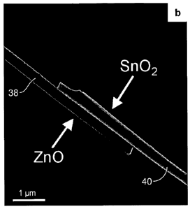
[0082] FIG. 7 illustrates successful optical coupling between a ZnO nanowire
38 and a Sn02 nanoribbon waveguide 40. FIG. 7A is a black and white
rendering of a true color dark-field/PL image of the nanowire 38 (56 pm long,
at top, pumped at 3.8 eV) channeling light into the nanoribbon 40 (265 pm
long, at bottom). The arrow denotes the location of the junction. FIG. 7B is
an
SEM image of the nanowire/nanoribbon junction. FIG. 7C illustrates spectra
of the coupled structures taken at different excitation and collection
locations.
From top to bottom: unguided PL of the ZnO nanowire; waveguided emission
from the ZnO nanowire collected at the bottom terminus of the nanoribbon;
waveguided emission from the Sn02 nanoribbon excited just below the
junction and collected at its bottom terminus; unguided PL of the Sn02
nanoribbon. Note that the emission from the ZnO nanowire is modulated
during its transit through the nanoribbon cavity.
[0083] FIG. 8 illustrates another example of a hetero-junction created between
-17-
CA 02565765 2006-11-03
WO 2005/114282 PCT/US2005/017029
a single ZnO nanowire and a Sn02 nanoribbon. FIG. 8A is a dark-field image
of the junction after pushing a ZnO nanowire up to the end facet of the Sn02
nanoribbon. The inset in FIG. 8A is a magnification of the active coupling
region showing the short (- 6-7 pm) ZnO nanowire and the upper terminus of
the Sn02 nanoribbon. The total length of the nanoribbon was - 600 pm. FIG.
8B shows spectra collected at the passive end (bottom terminus) while
pumping either the ZnO nanowire (On ZnO) or the SnO2 nanoribbon directly
(On NR). A profile of the band gap emission collected over the ZnO nanowire
(ZnO Only) is included for reference. The Modulation in the "On ZnO"
spectrum is a direct result of the broad emission from the ZnO propagating
through a high Q-factor Sn02 cavity.
[0084] The 50x dark-field image and 100x dark-field inset of FIG. 8A
pictorially
demonstrate the basic components of an active/passive nanophotonic device.
However, to ensure that we had devised a complete junction between the two
nanosystems, we optically pumped the ZnO nanowire active end and
collected at the passive Sn02 nanoribbon end. As seen in FIG. 8B, ZnO band
gap emission created from the pump source was directed across the
intervening air space by the ZnO cavity and into the neighboring SnO2
waveguide. The light output from the ZnO nanowire emerged at the distant
end of the nanoribbon and clearly showed a modulated emission profile
similar to the PL line shape seen in FIG. 4. This provides good evidence that
the light was in fact waveguided across hundreds of microns by the
nanoribbon cavity. To build like-material junctions, we employed a similar
manipulation scheme as described above. Two waveguiding nanoribbons
were coupled with their long axes collinear to each other by physically
sliding
a larger nanoribbon directly adjacent to the far end of a smaller nanoribbon.
[0085] FIG. 9 illustrates a SnO2/SnO2 junction created by coupling two
nanoribbon waveguides 42, 44 at their end facets. FIG. 9A and FIG. 9B are
dark-field images before (FIG. 9A) and after (FIG. 9B) completing a junction
between a large 42 (- 1 pm) and small 44 (- 400 nm) diameter nanoribbon.
FIG. 9C is a PL image of the same nanoribbon junction and end terminus
shown in FIG. 9B demonstrating that multi-junction networks between SnO2
-18-
CA 02565765 2006-11-03
WO 2005/114282 PCT/US2005/017029
nanoribbon waveguides can be realized.
[0086] The dark-field images in FIG. 9A and FIG. 9B capture the junction
before and after successfully adjoining the two nanoribbons. The PL image in
FIG. 9C verifies that light traveling down the small nanoribbon can be
directly
coupled into a secondary like-cavity. We are now building all-nanowire optical
circuits that operate via electron injection rather than optical pumping. The
oxide waveguides serve as important interconnects between active light
sources, such as LEDs and lasers, and optical detectors based on
photoconducting nanowires.
[0087] The optical loss of several nanoribbon waveguides was measured by
systematically varying the distance between UV excitation (50 pm spot size)
and PL collection in the near-field. We estimate a loss of about 2 dB mm-' at
a wavelength of 550 nm for a nanoribbon with a 400 x 150 nm2 cross-section,
which is significantly greater than losses reported recently for subwavelength
silica waveguides.
[0088] As can be seen from the forgoing, due to their extraordinary length,
high flexibility and strength, nanoribbon waveguides are excellent materials
with which to study the interplay between mechanics, microstructure and
optical confinement in nanoscale cavities: They can be manipulated and
assembled to serve as photonic interconnects between single nano-objects,
such as nanowire lasers, in optical circuits and devices.
[0089] Furthermore, nanoribbon waveguides can be used as filter devices.
For example, FIG. 10 illustrates the use of nanoribbons as short-pass filters.
FIG. 10A shows room temperature PL spectra of five different nanoribbons,
each 200 pm to 400 pm long, with 50% intensity cut-off wavelengths ranging
from 465 nm to 580 nm. Cross-sectional dimensions of the 465 nm, 492 nm,
514 nm, 527 nm and 580 nm filters were 310 nm x 100 nm (0.031 pm2), 280
nm x 120 nm (0.037 pmz), 350 nm x 115 nm (0.04 pmz), 250 nm x 225 nm
(0.056 Nm2), and 375 nm x 140 nm (0.053 pm2), respectively. The spectra
were normalized and offset for clarity. FIG. 10B shows a series of normalized
emission spectra taken of a single nanoribbon (315 pm x 355 nm x 110 nm)
-19-
CA 02565765 2006-11-03
WO 2005/114282 PCT/US2005/017029
as the pump spot was scanned away from the collection area. The unguided
PL curve-was obtained at a pump-probe separation of 50 pm. Larger
separations resulted in a progressive loss of the long wavelengths.
[0090] Example 1
[0091] Sn02 nanoribbon waveguides were synthesized by the chemical vapor
transport of SnO powder in a quartz tube reactor operating at 1100 C and
350 Torr of flowing argon (50 sccm). Milligram quantities of nanoribbons were
collected on an alumina boat near the center of the reactor and deposited
onto clean substrates by dry transfer. Long ZnO nanowires were grown via
oxidation of Zn metal in a quartz furnace at 800 C and 760 Torr of flowing
oxygen/argon, as described in the literature, and also dispersed by dry
transfer. InP nanowires produced by a laser-assisted vapor-liquid-solid
process (using Au catalyst) were sonicated into ethanol solution and
transferred to the surface by drop-casting. Contacts to InP were fabricated by
electron beam lithography and thermal evaporation (100 nm Ti), followed by
rapid thermal annealing at 475 C in N2/H2 for one minute.
[0092] Example 2
[0093] Optical measurements were carried out using a dark-field microscope
outfitted with a cryostat (Janis X-1 00). The PL excitation source was a HeCd
laser operating at 325 nm. Laser pointers (532 and 652 nm) and the HeCd
laser (442 nm) provided nonresonant illumination. The size of the laser spot
was -50 pm for all measurements. Spectra were collected with a fiber-
coupled spectrometer (SpectraPro 300i, Roper Scientific) and liquid N2 cooled
CCD detector. Images were captured using both a microscope-mounted
camera (CooISNAP, Roper Scientific) and a handheld digital camera (PRD-
T20, Toshiba). Loss measurements were made with a commercial NSOM
setup operating in collection mode, with 325 nm excitation. For nanoribbon
manipulation, we used a three-axis commercial unit tipped with tungsten
probes (10 pm ends).
[0094] As described above, photonic circuit elements can be assembled from
Sn02 nanoribbon and ZnO nanowire waveguides. High aspect ratio
nanoribbons/wires with diameters below the wavelength of light (typically 100
-20-
CA 02565765 2006-11-03
WO 2005/114282 PCT/US2005/017029
nm to 400 nm) were shown to act as excellent waveguides of both their own
internally generated photoluminescence (PL) and nonresonant UV/visible light
emitted from adjacent, evanescently coupled, nanowires or external laser
diodes. The length, flexibility and strength of these single-crystalline
structures enabled them to be manipulated and positioned on surfaces to
create various single-ribbon shapes and multi-ribbon optical networks,
including ring-shaped directional couplers and nanowire emitter-waveguide-
detector junctions. This ability to manipulate the shape of active and passive
nanowire cavities provides a new tool for investigating the cavity dynamics of
subwavelength structures. Moreover, future advances in assembling the
diverse set of existing nanowire building blocks could lead to a novel and
versatile photonic circuitry.
[0095] Waveguidi in Liquids
[0096] Quite surprisingly, we have also found that these one-dimensional (1 D)
nanostructures can guide light through liquid media. The fact that light can
be
delivered through these cavities in solution offers a unique application for
high
dielectric (n > 2) waveguides in fluidic sensing and probing. Waveguiding in
liquids is especially important for integrated on-chip chemical analysis and
biological spectroscopy in which small excitation and detection volumes are
required. Subwavelength nanostructures can be assembled to probe
molecules in a fluorescence or absorption scheme, both of which utilize the
decaying light field outside of the cavity to induce photon absorption. The
waveguide is strongly coupled to emitted photons near the cavity, allowing the
generated fluorescence to be directed back to the point of injection. Also,
the
nanoscale dimensions of the waveguides afford small liquid volumes
(-picoliters) to be sensed and presage the way for miniaturized optical
spectrometers.
[0097] Here, we also build upon the initial demonstration of nanowire/ribbon
photonic assembly with several proof-of-principle illustrations of optical
routing
between coupled nanowires. We first show that it is possible to deliver
individual nanosecond light pulses from lasing GaN and ZnO nanowires
-21-
CA 02565765 2006-11-03
WO 2005/114282 PCT/US2005/017029
through a nanoribbon waveguide; pulsed light must be transmissible if
nanowire photonic devices are to be useful in communications or computing.
Simple networks of Sn02 nanoribbons are then used to separate white light
and route individual colors based on a short-pass filtering effect. We also
describe an optical crossbar grid made of two pairs of orthogonal nanoribbons
that conducts light through abrupt 90 angles and provides a dramatic
example of the nature of optical confinement in these subwavelength cavities.
The fact that the waveguiding ability of our freestanding, flexible nanowires
and nanoribbons survives in liquid media suggests a role for nanowire light
delivery in microfluidics and biological applications.
Subwavelength Wayeguides as Ont ical Probes and Sensors
[0098] High dielectric subwavelength waveguides have a considerable
advantage for confining light in liquids over low dielectric waveguides such
as
silica-based structures. The low index contrast between the solution
(cladding) and silica core (ns;rca= 1.45) hinders efficient propagation of the
light
wave. FIG. 11 compares the photoluminescence (PL)/dark-field images of a
Sn02 nanoribbon (dimensions: 365 nm x 105 nm x 265 pm) resting on a
silicon oxide surface (1 pm thermal oxide) waveguiding in air (n = 1) and
water
(n = 1.33). The PL is generated with a CW HeCd laser (325 nm). FIG. 11
also shows how the guided PL spectrum of this thin nanoribbon changes
when it is immersed in water.
[0099] FIG. 1 1A is a combined PL/dark-field image of the nanoribbon 46 on a
dry oxide surface. The inset shows a magnified view of the blue end
emission. FIG. 11 B shows the same nanoribbon in a water environment,
under a quartz coverslip. The inset shows resultant green emission. FIG. 11 C
shows the spectra of the two situations. The large red shift of the empirical
cutoff wavelength (from 483 nm in air to -570 nm in water) is caused by the
decrease in refractive index profile between the substrate and the cap
medium. The more homogeneous cladding index improves wave confinement
in the nanoribbon core. The effect was reversible by evaporating the water.
[00100] As can be seen from FIG. 11 C, the spectra of the guided PL spectrum
broadens to longer wavelengths when it is covered by pure water. Such a red
-22-
CA 02565765 2006-11-03
WO 2005/114282 PCT/US2005/017029
shift would be anomalous for a fiber with a cladding of homogeneous
refractive index, where one expects the replacement of air (n=1) by water
(n=1.33) to increase losses and result in a blue shift of the mode cutoff.
However, when a slab or strip waveguide exists in an asymmetric cladding
environment (that is, when nWave9u;de > nsubtrace > ncover), as it does here,
raising
the index of the cover reduces its asymmetry with the substrate and improves
confinement.
[00101] Intuitively, the replacement of air (n=1) with water (n=1.33) on three
sides of a nanoribbon should increase its optical loss and hinder waveguiding,
especially for longer wavelengths. One would expect a narrowing of the
guided spectrum (a blue shift of the cutoff wavelength). Instead, we found
that the spectrum broadens to the red and the end emission changes from
blue in air to green in water. This surprising result, which seems to suggest
that a smaller index profile between core and cladding results in better, not
poorer, confinement, is likely a consequence of the smaller difference in
refractive index between water and the Si02 substrate than between air and
the substrate. The less anisotropic water-silica cladding shifts the modal
power nearer to the center of the nanoribbon and thereby reduces overall
radiative loss. Ribbons that were too large to show a cutoff for PL were
unaffected by immersion in water.
[00102] To demonstrate controlled manipulation of small volume, substrate
supported, liquid droplets, we placed an approximately 5 pL droplet of 1,5-
pentanediol on a silica substrate and then used a commercial
micromanipulator, equipped with an etched tungsten probe (tip diameter - 400
nm), to dice the large droplet into small volumes as shown in FIG. 12. FIG.
12A shows a dark-field image of various sized droplets of 1,5-pentanediol on
a silicon substrate (with a 1 pm thermal oxide). The radii and corresponding
volumes are displayed by each droplet. FIG. 12B is a magnified dark-field
image of smaller droplets (< 1 fL). The radii and corresponding volumes
(down to - 20 fL) are labeled on the dark-field image in FIG. 12A. Even
smaller volumes (< 1 fL) can be achieved with this method as shown in FIG.
12B. An alternative method to producing small volumes would be to use
-23-
CA 02565765 2006-11-03
WO 2005/114282 PCT/US2005/017029
microfluidic channels to mold the shape of the solution.
[00103] Ribbon waveguides can also sense molecules, proteins or larger
biological entities in solution by means of either an emission or absorption
mechanism as mentioned above. In the former, a nanoribbon provides local
excitation for fluorophores passing through the cone of scattered light at its
output end, and the emission is collected by a fiber or microscope.
[00104] Referring to FIG. 13, to demonstrate this fluorescence scheme, we
embedded the tip of a nanoribbon 48 in an approximately 3 pL to 5 pL droplet
of 1 mM Rhodamine 6G laser dye (R6G) in 1,5-pentanediol (n = 1.45). FIG.
13 shows fluorescence and absorbance detection of R6G with a nanoribbon
cavity. FIG. 13A is a fluorescence image of a droplet of 1mM R6G in 1,5-
pentanediol excited by blue light from a nanoribbon waveguide 48 (240 nm by
260 nm by 540 pm). The nanoribbon crosses the frame from upper left to
lower right. A notch filter was used to block the excitation light. The left
inset
of FIG. 13A is a dark-field image showing the droplet and the bottom half of
the nanoribbon. The right inset of FIG. 13A is a magnified view of the droplet
emission, showing the light cone and evanescent pumping of the dye along
the nanoribbon length. FIG 13B shows the spectra taken of the droplet
region (direct) and the fluorescence coupled back into the nanoribbon
(guided). The red shift of the guided emission is a microcavity effect. FIG.
13C is a dark-field image of the nanoribbon with a droplet deposited near its
middle (absorbance geometry). The nanoribbon was UV pumped on one side
of the droplet and probed on the other side, as indicated. FIG. 13D shows the
spectra of the guided PL without liquid present and with droplets of pure 1,5-
pentanediol and 1 mM R6G. The arrow indicates the absorption maximum of
R6G.
[00105] As can be seen, blue light (442 nm) launched into the far end of the
nanoribbon resulted in strong fluorescence from within the droplet, where the
R6G emission mapped out the spatial intensity distribution of the waveguide
output as a cone of light (FIG. 13A and Inset). A fraction of this
fluorescence
was captured by the nanoribbon cavity and guided back to its far end,
demonstrating that these waveguides are capable of routing signals both from
-24-
CA 02565765 2006-11-03
WO 2005/114282 PCT/US2005/017029
and to liquids. Spectra acquired from both ends of the nanoribbon are shown
in FIG. 13B. The guided fluorescence is red-shifted and somewhat sculpted
by its passage through the nanoribbon. However, there is little trace of the
heavy mode imprinting evident in, for example, FIG. 17F discussed below.
[00106] FIG. 13B also shows strong fluorescence originating from the segment
of the nanoribbon wet by the droplet through capillary action. Here, dye
molecules in proximity to the nanoribbon surface are excited in a
subwavelength version of total internal reflection fluorescence (TIRF). In
normal TIRF, excitation of a macroscopic waveguide (such as a microscope
coverslip) generates an evanescent field of light that decays exponentially
with
distance from the waveguide surface, limiting the depth of excitation to a
distance of -100 nm and enabling the local probing of structures such as cell
membranes. Because subwavelength fibers can carry a larger fraction of their
modal power outside of the core, they enhance the intensity of this
evanescent field and increase its penetration depth into the surroundings,
making proportionally more power available to excite nearby molecules.
Calculations indicate that roughly thirteen to fifteen per cent of the
electric field
intensity exists outside of the nanoribbon for the wavelength of light used in
this experiment. In this case, the radial field intensity decays to ten per
cent of
its maximum value at the center of the waveguide by about 135 nm into the
liquid solution. Since TIRF detection sensitivity scales with the fractional
power present in the waveguide cladding, one-dimensional nanostructures are
promising waveguides for local fluorescence sensing using this approach.
[00107] Another way that 1 D nanostructures may be used for optical detection
in solution relies on producing an absorption spectrum of molecules located
on and near the nanoribbon surface. Absorbance detection, while inherently
less sensitive than fluorescence methods, is applicable to a wider range of
molecules and avoids the complications of fluorescent tagging. We launched
white PL down a long nanoribbon (260 nm x 240 nm x 540 pm) onto the
midpoint of which a -1 pL droplet of 1 mM R6G (amaX = 535 nm) was
deposited (FIG. 13C). Dye molecules in the droplet imprinted their absorption
signature onto the propagating PL wave (double-Gaussian beam), completely
-25-
CA 02565765 2006-11-03
WO 2005/114282 PCT/US2005/017029
quenching transmission through the nanoribbon around the R6G absorption
maximum (FIG. 13D). Considering the dye concentration, droplet size and
spatial extent of the evanescent field, we estimate that less than forty
attomoles of dye (-24 million molecules) were probed in this experiment. We
have experimentally shown that sensitivities down to 50 pM (- 35,000
molecules) are easily attainable. We were able to detect dye concentrations
as low as 1 pM (24,000 molecules) using the same nanoribbon and a
comparable path length of -50 pm (not shown). Since this absorbance
approach also utilizes the evanescent fraction of the guided field, smaller
nanoribbons should again provide greater sensitivity. Other options for
improvement include altering the cavity shape to increase the probe length (as
discussed below), functionalizing the nanoribbon surface for selective
biosensing and launching multiple wavelengths for the simultaneous detection
of analytes with different electronic transitions. The next steps are to
integrate
subwavelength 1 D nanostructures into microfluidic devices and to apply them
as flexible probes in the study of live cells.
[00108] A third way that subwavelength nanoribbons/wires can be used for
chemical/biological sensing relies on the surface enhanced Raman
spectroscopic (SERS) effect. Surface-enhanced Raman scattering occurs
when an analyte molecules is probed in proximity to a metal surface (usually
Cu, Ag or Au) that serves to massively enhance the local electromagnetic field
through resonance with the surface plasmons of the metal. The resulting
Raman signal of the analyte can be enhanced by a factor of up to 1014, which
allows single-molecule sensing in many cases. The nanoribbons/wires
described here were fashioned into subwavelength SERS fibers by decorating
their surfaces with a high density of silver nanoparticles. By exposing the
nanoparticles-coated nanoribbon/wire to an analyte solution while injecting
monochromatic light down the nanoribbon/wire, it is possible to detect the
SERS signal of the analyte molecule. This concept allows "fingerprint"
identification of analyte molecules based on their SERS vibrational
signatures,
using a subwavelength waveguide for light introduction and confinement. FIG.
14A shows a schematic picture of this concept, while FIG. 14B and FIG. 14C
-26-
CA 02565765 2006-11-03
WO 2005/114282 PCT/US2005/017029
show an image of a nanoribbon (NR) coated with 40 nm silver nanoparticles
attached by exposing the nanoribbon to a flowing nanoparticle solution. The
particles are seen to scatter the waveguided light very effectively. By then
exposing the structure to an analyte solution of interest, it is possible to
generate a SERS signal. The device is reusable by simply dissolving the Ag
nanoparticles in an acidic solution (e.g., HNO3) and then reintroducing fresh
Ag particles.
[00109] The devices shown thus far all operate under single pass geometries.
Multi-pass structures would increase sampling lengths and ultimately lead to a
more sensitive spectrometer. FIG. 15 shows a PL/dark-field image of two
nanoribbons (NR1 and NR2) evanescently coupled at arrow 1. The top inset is
a magnified dark-field image of the coupled nanoribbons with a glycol droplet
designating where the analyte would sit in this configuration. The bottom
inset
is a dark-field image of NR1 with NR2 removed showing a coupled ring
structure (junction - denoted be arrow 2) that would serve as a multi-pass
beam path in a subwavelength optical spectrometer.
[00110] FIG. 15 illustrates that ring shapes can be easily fashioned using our
manipulation capabilities to create a subwavelength cavity shape that would
sample an analyte repetitively. The glycol droplet (top inset) serves to
identify
where the analyte would sit in this particular configuration. The PL/dark-
field
image shows a two nanoribbon device evanescently coupled (arrow 1 denotes
the junction), illustrating the first step to design a multi-pass spectrometer
based on free-standing 1 D nanostructures. The bottom inset was taken after
manipulating the end of NR1 into a ring structure (arrow 2 denotes the
junction) showing the second step for creating a multi-cycle instrument.
Additional work is necessary to fully realize better sensitivity from these
advanced designs, but previous results on coupling efficiencies suggest up to
an order of magnitude increase from a multi-pass geometry.
[00111] We note that the fabrication of a practical subwavelength fiber
spectrometer as introduced above would benefit from a more controlled flow-
cell type microfluidic design in which the sensing nanoribbon/wire is
integrated
with microfluidic channels for solution introduction. We have built such an
-27-
CA 02565765 2006-11-03
WO 2005/114282 PCT/US2005/017029
integrated device using a poly-dimethylsiloxane (PDMS) stamp patterned with
flow channels to control analyte flow past an embedded nanoribbon/wire
waveguide. With this microfluidic design, we can pulse multiple analyte
solutions past a well-defined section of a sensing nanoribbon/wire, permitting
reuse of the sensor for biological and other liquid-based monitoring uses.
FIG. 16 shows the microfluidic channels (MFC) of a PDMS stamp bridged by
multiple nanoribbons (NR). This is shown schematically in FIG. 16A. FIG. 16B
is an image showing microfluidic channels in detail and FIG. 16C is an image
showing several nanoribbons bridging the microfluidic channels shown in FIG.
16B. This microfluidic layout is important for the practical use of these
structures for fluorescence, absorbance and SERS sensing.
[00112] It should be noted that the ideas and principles set forth herein for
chemically synthesized 1 D semiconductor nanostructures are entirely
compatible with existing lithography techniques. State-of-the-art electron
beam and other lithography methods currently offer better size control,
reproducibility, and processing speeds to produce subwavelength optical
probes and spectrometers than the serial approach discussed here. Future
experiments will include lithographically defined structures on various
support
substrates to discern the limits of detection using nanoscale optics.
[00113] In terms of present industrial efforts and interests in small volume
detection, NanoDrop Technologies has developed a UVNis spectrometer
(ND-1000) based on patented sample retention technology. The instrument is
generally used to detect 1 pL to 2 pL nucleic acid aliquots with a sample
detection limit of 2 ng/pL (dsDNA). The path length for the Xe flash lamp (220
nm to 750 nm) is held relatively fixed at 1 mm. The major advantages of a
subwavelength spectrometer over the commercially available unit is smaller
volume size (- 106 times smaller), shorter path lengths (- 10 times shorter),
and possibly higher sensitivity with the advanced multi-pass geometries.
Optical Routing With Nanoribbons And Nanowire Assemblies
[00114] The manipulation of optical energy in structures smaller than the
wavelength of light is key to the development of integrated photonic devices
for computing, communications and sensing. We assembled small groups of
-28-
CA 02565765 2006-11-03
WO 2005/114282 PCT/US2005/017029
freestanding, chemically synthesized nanoribbons and nanowires into model
structures that illustrate how light is exchanged between subwavelength
cavities made of three different semiconductors. The strength of the optical
linkages formed when nanowires are brought into contact depends both on
their volume of interaction and angle of intersection. Using simple coupling
schemes, lasing nanowires can launch coherent pulses of light through
nanoribbon waveguides that are up to several millimeters in length. Also,
inter-wire coupling losses are low enough to allow lightto propagate across
several right-angle bends in a grid of crossed nanoribbons. The fraction of
the
guided wave power traveling outside the nanowire/nanoribbon cavities is
utilized to link nanowires through space and to separate colors within multi-
ribbon networks. In addition, we find that nanoribbons function excellently as
waveguides in liquid media and provide a unique way to probe molecules in
solution or in proximity to the waveguide surface. Our results lay the
groundwork for photonic devices based on assemblies of active and passive
nanowire elements and presage the use of nanowire waveguides in
microfluidics and biology.
[00115] Example 3
[00116] Sn02 nanoribbons were synthesized by the chemical vapor transport of
SnO at 1100 C in flowing argon. ZnO nanowires were grown as epitaxial
arrays on sapphire substrates by the oxidation of metallic zinc at 800 C,
using
gold as a catalyst. GaN nanowires were made by the chemical vapor
transport of gallium in a NH3/H2 mixture at 900 C, with nickel as the
catalyst.
The Sn02 nanoribbons were dry transferred en masse to oxidized silicon
substrates (600 nm Si02, Silicon Sense Inc.). A triple-axis micromanipulator
tipped with a tungsten probe (-400 nm tip diameter) was used to remove
individual ZnO and GaN nanowires (chosen by their PL spectra) from their
growth substrates and then deposit them with the nanoribbons.
[00117] Example 4
[00118] Nanoribbons and nanowires were manipulated with the probe under a
dark-field microscope. A HeCd laser provided continuous wave (CW) resonant
'illumination (325 nm), while the fourth-harmonic of a Nd:YAG laser (266 nm, 8
-29-
CA 02565765 2006-11-03
WO 2005/114282 PCT/US2005/017029
nm, 10 Hz) was used for pulsed pumping. Laser diodes (652 nm and 532 nm)
and the HeCd laser (442 nm) supplied visible light for the filtering and
fluorescence demonstrations. The lasers were focused to a beam diameter of
approximately 50 m, giving a CW power density of approximately 175 W/cmZ
and a pulsed energy density of approximately 10 pJ/cm2. Spectra were
acquired with a fiber-coupled spectrometer (gratings at 150 and 1200
grooves/mm, SpectraPro 300i, Roper Scientific) and liquid N2-cooled CCD
setup. Black-and-white and color images were recorded with two microscope-
mounted CCD.cameras (CoolSnap fx and CoolSnap cf, Photometrics).
[00119] Many of the nanoribbons/wires described herein operated as single-
mode fibers for some of the experimental wavelengths, while others were
multi-mode. For reference, the approximate single-mode cutoff diameters of a
cylindrical step-index fiber in air are 140 nm (A = 365 nm) and 265 nm (A =
600 nm) for Sn02, 112 nm (A = 365 nm) for GaN, and 140 nm (A = 380 nm)
and 220 nm (A = 510 nm) for ZnO .
[00120] In the liquid experiments, large droplets (-5 pL) of water or various
alcohols were transferred to the oxide surface by pipette. The solvent
droplets
were then diced into smaller volumes (as small as 100 fL) and positioned on
the surface using the manipulator.
[00121] Nanoribbon and nanowire sizes were determined with a scanning
electron microscope (SEM).
[00122] FIG. 17 and FIG. 18 document several experiments that were
performed with a single nanoribbon in various combinations with GaN and
ZnO nanowires.
[00123] FIG. 17 illustrates the routing of GaN PL and lasing emission. FIG.
17A is a dark-field optical image of a coupled GaN nanowire 50 and Sn02
nanoribbon 52. The label A denotes the location of the junction. FIG. 17B
shows direct excitation of the Sn02 nanoribbon at location B generates white
PL that is guided to the ends of the Sn02 cavity. Some of the light is
scattered by a large particle found at C. The inset in FIG. 17B is a magnified
view of the bottom emission spot. FIG. 17C is a magnified view of the junction
area. The inset in FIG. 17C is a SEM image showing that the two structures
-30-
CA 02565765 2006-11-03
WO 2005/114282 PCT/US2005/017029
are staggered over 9 m and touch for approximately 2 m. FIG. 17D shows
direct CW excitation of the GaN nanowire generates UV band-edge emission
at 365 nm and a small amount of visible defect emission at 650 nm. The
cavity is too thin to permit the confinement of red light, but (Inset) a UV
camera detects strong waveguiding of the UV PL. FIG. 17E is an optical
image of the routing of UV laser pulses from nanowire to nanoribbon. Here,
the GaN cavity was pumped above its lasing threshold by a pulsed 266 nm
source (itself invisible to this detector). FIG. 17F shows spectra comparing
the GaN PL and lasing emission before and after passage through the
nanoribbon cavity. The broad pseudo-Gaussian spontaneous emission peak
(top) is broken into a series of sharp modes during its transit through the
nanoribbon (WG PL). Likewise, the lasing emission at moderate pump power,
which shows multiple modes (GaN lasing), is severely modulated by the mode
structure of the Sn02 cavity (bottom). Spectra are normalized and offset for
clarity.
[00124] As can be seen, FIG. 17A shows a GaN.nanowire (130 nm by 65 m)
that has been coupled to a Sn02 nanoribbon (240 nm by 260 nm by 460 m)
with the micromanipulator. The magnified SEM view of the GaN-Sn02
junction (Inset, FIG. 17B) indicates that the two structures are in physical
contact over an interaction length of approximately 2 m. This staggered-
bonded configuration provides good optical coupling between the cavities and
some degree of inter-wire adhesion (via electrostatic forces), which aids in
the
construction of multi-wire networks. Butt-end coupling is also effective, and
it
is possible for us to detect the transfer of light between nanowire cavities
that
are weakly coupled across an air gap of up to several hundred nanometers
(not shown). If two nanoribbons are crossed instead of staggered, the
coupling losses decrease with shallower intersection angles, which has also
been observed recently for crossed CdS nanowires.
[00125] To demonstrate the routing of continuous wave light, we excited the
GaN nanowire with the focused beam of a HeCd laser operating at 325 nm.
Band-edge PL from the GaN cavity was channeled through the Sn02
nanoribbon to emerge primarily at its far end. A fraction of the light was
also
-31-
CA 02565765 2006-11-03
WO 2005/114282 PCT/US2005/017029
scattered by imperfections along the length of the nanoribbon (i.e., attached
particles or macroscopic step edges). Far-field spectra collected from the
output end of the nanoribbon (FIG. 17F) show that the quasi-Gaussian PL
band of GaN is imprinted with the mode structure of the Sn02 cavity during its
transit. This mode structure is not longitudinal (Fabry-Perot) in nature, as
it is
for shorter nanowires; instead, it is a complex interference pattern dependent
on nanoribbon shape and cross-sectional dimensions, among other factors.
[00126] Moreover, referring also to FIG. 18, it is possible to simultaneously
guide the output of two (or more) nanolasers by coupling multiple ZnO and
GaN nanowires to the same nanoribbon, opening up the possibility of
performing nonlinear wave mixing within single nanocavities. FIG. 18A is a
dark-field image of a GaN nanowire 54 and a ZnO nanowire 56 coupled to the
same nanoribbon 58. The scale bar is 10 pm. FIG. 18B shows the spectrum
of guided light collected at the far end of the nanoribbon when both nanowires
were pumped above their lasing thresholds by the same train of optical
pulses. The nanoribbon is the same used in FIG. 13 and FIG. 17.
[00127] Note that in contrast to their continuous wave emission, the pulsed
emission of ZnO and GaN is nearly devoid of visible PL since the defect
bands experience no gain. This is experimental verification that coherent
optical pulses can be transferred between nanowires and steered hundreds of
micrometers from their source. With high frequency electrical pumping,
nanowire laser/waveguide combinations could be used to transduce and
shuttle packets of electro-optical information within future computing and
communications devices.
[00128] FIG. 19 illustrates GaN nanowire lasing. FIG. 19A shows a series of
emission spectra at different pump fluence for an isolated GaN nanowire with
a diameter of 150 nm and length of 45 m. The inset in FIG. 19A shows the
PL spectrum. FIG. 19B shows the energy curve for the same nanowire.
Typical thresholds for GaN NW lasing were 5 J to 15 J cm-2. The inset in
FIG. 19B is an image of lasing emission from a different GaN nanowire,
showing its pronounced spatial pattern. By pumping the GaN nanowire above
its lasing threshold (-5 NJ/cm2) with pulsed UV excitation, we were able to
-32-
CA 02565765 2006-11-03
WO 2005/114282 PCT/US2005/017029
send single optical pulses from the nanowire laser through the nanoribbon
waveguide (FIG. 17E). The spectrum of several thousand accumulated pulses
(FIG. 17F) shows a series of sharp modes (FWHM = 0.8 nm) slightly red-
shifted from the band edge of GaN. These are the Fabry-Perot type lasing
modes of the GaN nanowire resonator, modulated in intensity by the
nanoribbon cavity. We have obtained similar results with junctions between
nanoribbons and lasing ZnO nanowires.
[00129] Referring now to FIG. 20 and FIG. 21, since diffraction losses in a
subwavelength cavity increase markedly with wavelength, a nanoribbon
waveguide preferentially confines the bluer portion of any non-monochromatic
beam. As a result, nanoribbons act as short-pass filters with cutoff
wavelengths that are determined by their cross-sectional dimensions and
overall length.
[00130] FIG. 20 shows color filtering in a nanoribbon network 60. FIG. 20A is
a
dark-field image of a four-ribbon assembly as it guides white PL generated at
the pump spot (left) and separates it into a different color at the end of
each
nanoribbon (right). The scale bar is 50 pm. FIG. 20B is a magnified view of
the emission region. The branch nanoribbons 1-3 in FIG. 20B emitted green,
aqua and blue light because of their progressively smaller cross-sections (350
nm by 140 nm, 260 nm by 175 nm and 210 nm by 135 nm, respectively).
Their 50% cutoff wavelengths were determined by near-field scanning optical
microscopy (NSOM) to be 543 nm, 502 nm and 478 nm. The stem nanoribbon
is 260 nm by 240 nm by 390 pm. FIG. 20C shows that non-resonant blue light
is transmitted to the end of all four nanoribbons, while FIG. 20D shows that
green light is much more strongly guided by nanoribbon 1 than by nanoribbon
3 and FIG. 20E shows that red light is filtered out by all three branches. The
scale bar is 20 pm.
[00131] As can be seen from FIG. 20, we assembled a simple network
comprising four nanoribbons of different sizes to show how such a structure
may be used to separate colors. When excited at 325 nm, the large
nanoribbon that formed the stem of the network 60 emitted white light
composed of two broad Sn02 PL bands centered at 495 nm and 590 nm, as
-33-
CA 02565765 2006-11-03
WO 2005/114282 PCT/US2005/017029
can be seen from FIG. 21 which is a typical PL spectrum of a Sn02
nanoribbon showing its two defect bands. Varying amounts of the stem
emission then flows into the three shorter and consecutively thinner branch
nanoribbons, separating the white light into green, aqua and blue components
(ribbons 1-3). Alternatively, when monochromatic red light was launched into
the stem only the stem nanoribbon lit up, while green light was guided
strongly
(weakly) by the largest (smallest) branch and blue light passed through all
three branches as well as the stem (FIG. 20B-20D). Although this color
filtering effect works only in short-pass mode, and so cannot, for instance,
isolate the pure red component of a white beam, it may prove useful in such
tasks as removing visible contamination from UV pulses or providing local
excitation for fluorophores with narrow absorption bands, such as quantum
dots.
[00132] Referring to FIG. 22, to test the limits of inter-cavity optical
coupling, we
assembled four nanoribbons into a rectangular grid (46 m long by -25 m
wide) featuring X-junction vertices with small contact areas (< 0.15 m) (FIG.
22A and Inset). FIG. 22A is a dark-field image of the four-ribbon structure,
with the input channel extending off the frame to the right and the output
channels labeled 1-7. The nanoribbons vary in size from 300-400 nm on a
side. (FIG. 22A and Inset). A SEM image of the junction at the lower right
vertex. FIG. 22B is a PL image as the input channel is pumped at 325 nm.
Light is.guided to the seven output ends with different intensities and colors
as
described below.
[00133] The structure was designed with one long channel for light input and
seven short output channels that could be monitored simultaneously. As
shown in FIG. 22B, direct excitation of the input channel triggered emission
from all seven of the nanoribbon outputs, with the following intensity
distribution: 1 6 > 4= 7> 3 > 5 > 2. This is exactly the sequence one would
expect after considering the trajectory of the incoming light and the
intensity of
scattering at the four nanoribbon-ribbon junctions. The light trajectory is
important here since the low reflectivity of their end facets makes
nanoribbons
poor resonators (with an ideal finesse of -1.3). As such, most photons do not
-34-
CA 02565765 2006-11-03
WO 2005/114282 PCT/US2005/017029
make multiple passes and light flow is highly directional. The right-angle
intersections present significant obstacles to inter-cavity waveguiding by
total
internal reflection. At the same time, they act as quasi-isotropic scatterers
that feed light between nanoribbons. Nanoribbon-to-ribbon losses, although
nearly maximized in this geometry, are still low enough for the activation of
channels 2 and 3, which require photons to negotiate two right-angle junctions
and transit three separate cavities. When we added a ZnO nanowire laser to
the input channel and used it to launch light into the grid, emission was
detected from all channels but 2 and 3; the number of injected photons was
simply too small to illuminate the parallel nanoribbon. Nanowire grids have
already been employed to implement rudimentary electronic logic. Integrated
optical logic and all-optical switches present exciting prospects, and our
results show that grids of nanowires should be capable of routing signals for
such tasks.
[00134] Due to their high refractive indices (n ? 2), the nanoribbons and
nanowires discussed here function well as waveguides in water and other
liquids. This is a considerable advantage over subwavelength silica
waveguides, which cannot efficiently confine visible light in liquids because
of
a low dielectric contrast (ns;i;ca = 1.45). Waveguiding in liquids is
especially
important for integrated on-chip chemical analysis and biological spectroscopy
in which small excitation and detection volumes are required.
[00135] As can be seen, chemically synthesized nanoribbon and nanowire
waveguides have two unique and potentially useful features for
subwavelength photonics applications. First, nanowires push subwavelength
optical fibers beyond silica. The scores of materials that can now be made in
nanowire form include active, passive, nonlinear and semiconducting
inorganic crystals, as well as a wide variety of polymers. Simultaneous
photon, charge carrier and spin manipulation is possible within and between
nanowires of different compositions. Also, many of these materials have
higher refractive indices than silica-based glasses, permitting light of a
given
wavelength to be confined within thinner structures for denser integration.
This
enables waveguiding in liquids and makes it possible to extend
-35-
CA 02565765 2006-11-03
WO 2005/114282 PCT/US2005/017029
subwavelength guiding to telecommunications wavelengths using, for
example, an approximately 300 nm diameter Si or GaP nanowires. Second,
nanowires are freestanding, mechanically flexible elements that can be
manipulated on surfaces or used as mobile probes in fluids. As such, they
offer a type of versatility difficult to achieve with lithographically-defined
structures that are permanently affixed to their substrates.
[00136] The disadvantages of nanowire photonics include (i) the paucity of
parallel assembly methods for accurately arranging large groups of nanowires
into useful structures; (ii) relatively high inter-wire coupling losses
compared to
monolithic waveguides formed by lithography (coupling losses could be greatly
reduced if branched, multi-component nanowires were developed to replace
the staggered or crossed nanowire cavities used here); (iii) the lesser
geometric perfection of nanowire assemblies relative to the precise shapes
and sizes definable with lithography. Geometric imprecision introduces some
uncertainty in the resulting light propagation and adds complexity to nanowire
experiment/theory comparisons. However, despite these limitations,
nanowires and their assemblies provide an important new platform for
photonics studies and applications that is only beginning to be investigated.
[00137] It will be appreciated that the subwavelength waveguide described
herein can be used as a functional element in photonic circuits such as
optical
networks, optical filters, optical directional couplers, emitter-waveguide-
detector junctions, optical probes, optical sensors, optical routers, optical
junctions, optical modulators, optical Y-junctions, optical branch networks,
Mach-Zehnder interferometers, optical ring oscillators, nanolasers, optical
phase shifters, fluidic sensors, fluidic probes, microfluidic devices, optical
spectrometers, and optical crossbar grids. Those skilled in the art will also
appreciate that the nanostructures described herein can be fabricated and
incorporated into devices, systems and structures using various techniques
known in the art. Additionally, reference is made to U.S. Patent No.
6,882,051, entitled "NANOWIRES, NANOSTRUCTURES AND DEVICES
FABRICATED THEREFROM" issued on April 19, 2005, which is incorporated
herein by reference in its entirety, and to U.S. Patent Application
Publication
-36-
CA 02565765 2006-11-03
WO 2005/114282 PCT/US2005/017029
No. US 2004/0131537 Al, entitled "FUNCTIONAL BIMORPH COMPOSITE
NANOTAPES AND METHODS OF FABRICATION" published on July 8,
2004, also incorporated herein by reference in its entirety.
[00138] Although the description above contains many details, these should not
be construed as limiting the scope of the invention but as merely providing
illustrations of some of the presently preferred embodiments of this
invention.
Therefore, it will be appreciated that the scope of the present invention
fully
encompasses other embodiments which may become obvious to those skilled
in the art, and that the scope of the present invention is accordingly to be
limited by nothing other than the appended claims, in which reference to an
element in the singular is not intended to mean "one and only one" unless
explicitly so stated, but rather "one or more." All structural, chemical, and
functional equivalents to the elements of the above-described preferred
embodiment that are known to those of ordinary skill in the art are expressly
incorporated herein by reference and are intended to be encompassed by the
present claims. Moreover, it is not necessary for a device or method to
address each and every problem sought to be solved by the present invention,
for it to be encompassed by the present claims. Furthermore, no element,
component, or method step in the present disclosure is intended to be
dedicated to the public regardless of whether the element, component, or
method step is explicitly recited in the claims. No claim element herein is to
be construed under the provisions of 35 U.S.C. 112, sixth paragraph, unless
the element is expressly recited using the phrase "means for."
-37-