Note: Descriptions are shown in the official language in which they were submitted.
CA 02566361 2012-08-07
1
WIDE BANDGAP TRANSISTORS WITH MULTIPLE
FIELD PLATES
BACKGROUND OF THE INVENTION
Field of the Invention
The present invention relates to transistors and
particularly to transistors utilizing field plates.
Description of the Related Art
Improvements in the manufacturing of AlGaN/GaN
semiconductor materials have helped advance the
development of AlGaN/GaN transistors, such as high
electron mobility transistors (HEMTs) for high frequency,
high temperature and high power applications. AlGaN/GaN
has large bandgaps, high peak and saturation electron
velocity values [B. Gelmont, K. Kim and M. Shur, Monte
Carlo Simulation of Electron Transport in Gallium
Nitride, J.Appl.Phys. 74, (1993), pp. 1818-1821].
AlGaN/GaN HEMTs can also have 2DEG sheet densities in
excess of 1013cm-2 and relatively high electron mobility
(up to 2019 cm2/Vs) [R. Gaska, et al., Electron Transport
in AlGaN-GaN Heterostructures Grown on 6H-SiC Substrates,
Appl.Phys.Lett. 72, (1998), pp. 707-709].
These
characteristics allow AlGaN/GaN HEMTs to provide very
CA 02566361 2006-11-08
W02005/114743 PCT/US2005/012821
2
high voltage and high power operation at RF, microwave
and millimeter wave frequencies.
AlGaN/GaN HEMTs have been grown on sapphire
substrates and have shown a power density of 4.6 W/mm and
a total power of 7.6 W [Y.F. Wu et al., GaN-Based FETs
for Microwave Power Amplification, IEICE Trans. Electron.
E-82-C, (1999). pp. 1895-1905]. More recently, AlGaN/GaN
HEMTs grown on SIC have shown a power density of 9.8 W/mm
at 8 GHz [Y.F. Wu, et al., Very-High Power Density
AlGaN/GaN HEMTs, IEEE Trans.Electron.Dev. 48, (2001), pp.
586-590] and a total output power of 22.9 W at 9 GHz [M.
Micovic, et al., AlGaN/GaN Heterojunction Field Effect
Transistors Grown by Nitrogen Plasma Assisted Molecular
Beam Epitaxy, IEEE Trans.Electron.Dev.48, (2001), pp.
591-5961.
U.S. Patent number 5,192,987 to Khan et al.
discloses GaN/AlGaN based HEMTs grown on a buffer and a
substrate. Other AlGaN/GaN HEMTs and field effect
transistors (FETs) have been described by Gaska et al.,
High-Temperature Performance of AlGaN/GaN HFET1 s on SiC
Substrates, IEEE Electron Device Letters, 18, (1997), pp.
492-494; and Wu et al. "High Al-content AlGaN/GaN HEMTs
With Very High Performance", IEDM-1999 Digest, pp. 925-
927, Washington DC, Dec. 1999. Some of these devices have
shown a gain-bandwidth product (fT) as high as 100
gigahertz (Lu et al. "AlGaN/GaN HEMTs on SIC With Over
100 GHz ft and Low Microwave Noise", IEEE Transactions on
Electron Devices, Vol. 48, No. 3, March 2001, pp. 581-
585) and high power densitie up to 10 W/mm at X-band (Wu
et al., "Bias-dependent Performance of High-Power
AlGaN/GaN HEMTs", IEDM-2001, Washington DC, Dec. 2-6,
2001) and Wu et al., High Al-Content AlGaN/GaN MODFETs
CA 02566361 2012-08-07
3
for Ultrahigh Performance, IEEE Electron Device Letters
19, (1998), pp. 50-53].
Electron trapping and the resulting difference
between DC and RF characteristics have been a limiting
factor in the performance of these devices. Silicon
nitride (SiN) passivation has been successfully employed
to alleviate this trapping problem resulting in high
performance devices with power densities over 10W/mm at
Ghz. For example, U.S. Patent No. 6,586,781 discloses
10
methods and structures for reducing the trapping effect
in GaN-based transistors. However, due to the high
electric fields existing in these structures, charge
trapping is still an issue.
Field plates have been used to enhance the
performance of GaN-based HEMTs at microwave frequencies
[See S Kamalkar and U.K. Mishra, Very High Voltage
AlGaN/GaN High Electron Mobility Transistors Using a
Field Plate Deposited on a Stepped Insulator, Solid State
Electronics 45, (2001), pp. 1645-1662]. These approaches,
however, have involved a field plate connected to the
gate of the transistor with the field plate on top of the
drain side of the channel. This can result in a
significant field plate to drain capacitance and the
field plate being connected to the gate adds additional
gate-to-drain capacitance (Cgd) to the device. This can
not only reduce gain, but can also cause instability due
to poorer input-output isolation.
SUMMARY OF THE INVENTION
The present invention provides transistors with
multiple field plates, the topmost of which is
electrically connected to the source electrodes with the
CA 02566361 2006-11-08
PCT/US2005/012821
WO 2005/114743
4
intermediate ones being connected to the source or gate
electrodes. One embodiment of a transistor according to
the present invention comprises an active region. Source
and drain electrodes are formed in contact with. the
active region and a gate is formed between the source and
drain electrodes on active region. A plurality of spacer
layers and field plates are included, the first of the
spacer layers being on at least part of the surface of
the active region between the gate and the drain and
source electrodes and the first of the field plates on
the first of the spacer layers. The remaining spacer
layers and field plates are arranged alternately over the
first of spacer layers and the first of the field plates
with the topmost of the field plates electrically
connected to the source electrode and each of the field
plates below electrically connected to the gate or source
electrode.
Another embodiment of a transistor according to the
present invention comprises an active region, with source
and drain electrodes in contact with the active region. A
gate is between the source and drain electrodes and on
the active region. A plurality of field plates are
arranged over the active region, each of which extends
from the edge of the gate toward the drain electrode, and
each of which is isolated the active region and from the
others of the field plates. The topmost of the field
plates is electrically connected to the source electrode
and each of the others of the field plates are
electrically connected to the gate or the source
electrode.
These and other further features and advantages of
the invention would be apparent to those skilled in the
CA 02566361 2006-11-08
WO 2005/114743 PCT/US2005/012821
art from the following detailed description, taking
= together with the accompanying drawings, in which:
BRIEF DESCRIPTION OF THE DRAWINGS
5 FIG. 1 is a plan view of one embodiment of a HEMT
according to the present invention;
FIG. 2 is a sectional view of one embodiment of a
HEMT according to the present invention;
FIG. 3 is a plan view of another embodiment of a
HEMT according to the present invention;
FIG. 4 is a plan view of another embodiment of a
HEMT according to the present invention;
FIG. 5 is a sectional view of another embodiment of
a HEMT according to the present invention;
FIG. 6 is a plan view of another embodiment of a
HEMT according to the present invention;
FIG. 7 is a sectional view of one embodiment of a
MESFET according to the present invention;
FIG. 8 is a sectional view of another embodiment of
a MESFET according to the present invention;
FIG. 9 is a sectional view of another embodiment of
a HEMT according to the present invention;
FIG. 10 is a table comparing the operating
characteristics of a HEMT according to the present
invention compared to a HEMT with no field plate, a HEMT
with a gate connected field plate and a HEMT with a
source connected field plate;
FIG. 11 is a sectional view of another embodiment of
a HEMT according to the present invention having a gamma
gate; and
FIG. 12 is a sectional view of another embodiment of
a HEMT according to the present invention having a
recessed gate.
CA 02566361 2006-11-08
WO 2005/114743 PCT/US2005/012821
6
DETAILED DESCRIPTION OF THE INVENTION
The multiple field plate arrangements according to
the present invention can be used with many different
transistor structures, such as transistor structures made
of wide bandgap materials. Transistors generally include
an active region comprising semiconductor layers, with
metal source and drain electrodes formed in electrical
contact with the active region, and a gate formed between
the source and drain electrodes for modulating electric
fields within the active region. A first spacer layer is
formed above the active region, over at least a portion
of the surface of the active region between the gate and
the drain. The first spacer layer can comprise a
dielectric layer, or a combination of multiple dielectric
layers. The first spacer layer preferably covers the gate
and the topmost surface of the active region between the
gate and source and drain electrodes, although as
described below it can cover less.
A conductive first field plate is formed on the
first spacer layer with the first spacer layer providing
isolation between the field plate and the gate and active
region below. The first field plate extends a distance Lf1
from the edge of the gate toward the drain electrode.
The first field plate can be electrically connected to
either the source electrode or the gate.
A second spacer layer is formed over at least part
of the first field plate and part of the surface of the
first spacer layer between the gate and the drain
electrode. In a preferred embodiment, however the second
spacer covers the first field plate and the top exposed
surfaces of the transistor structure, which is typically
the first spacer layer. A second field plate is formed on
=
CA 02566361 2006-11-08
WO 2005/114743 PCT/US2005/012821
7
the second spacer layer with the second spacer layer
providing isolation between the first and second field
plates, and depending on the coverage of the first spacer
layer, isolation between the gate and active region.
Other transistor structures according to the present
invention can have more than two field plates. The
topmost field plate is typically electrically connected
to the source electrode, while the intermediate field
plates are electrically connected to either the gate or
the source electrode.
This field plate arrangement can reduce the peak
electric field in the device, resulting in increased
breakdown voltage and reduced trapping. The reduction of
the electric field can also yield other benefits such as
reduced leakage currents and enhanced reliability. By
having the field plate electrically connected to the
source electrode, the reduced gain and instability
resulting from gate connected field plates is reduced.
When arranged according to the present invention, the
shielding effect of a source-connected field plate can
reduce Cgd, which enhances input-output isolation.
One type of transistor that can utilize the multiple
field plate arrangement according to the present
invention is a high electron mobility transistor (HEMT),
which typically includes a buffer layer and a barrier
layer on the buffer layer. A two dimensional electron gas
(2DEG) layer/channel is formed at the heterointerface
between the buffer layer and the barrier layer. A gate
electrode is formed on the barrier layer between source
and drain electrodes. The HEMT also includes the multiple
spacer layer and field plate arrangement described above.
Another type of transistor that can utilize the
multiple field plate arrangement according to the present
CA 02566361 2006-11-08
WO 2005/114743 PCT/US2005/012821
8
invention is a field effect transistor and particularly a
metal semiconductor field effect transistor (MESFET),
which typically includes a buffer layer and a channel
layer on the buffer layer. A gate is formed on the
channel layer between source and drain electrodes and the
MESFET also includes the multiple spacer layer and field
plate arrangement described above.
It will be understood that when an element or layer
is referred to as being "on", "connected to", "coupled
to" or "in contact with" another element or layer, it can
be directly on, connected or coupled to, or in contact
with the other element or layer or intervening elements
or layers may be present. In contrast, when an element
is referred to as being "directly on," "directly
connected to", "directly coupled to" or "directly in
contact with" another element or layer, there are no
intervening elements or layers present. Likewise, when a
first element or layer is referred to as being "in
electrical contact with" or "electrically coupled to" a
second element or layer, there is an electrical path that
permits current flow between the first element or layer
and the second element or layer. The electrical path may
include capacitors, coupled inductors, and/or other
elements that permit current flow even without direct
contact between conductive elements.
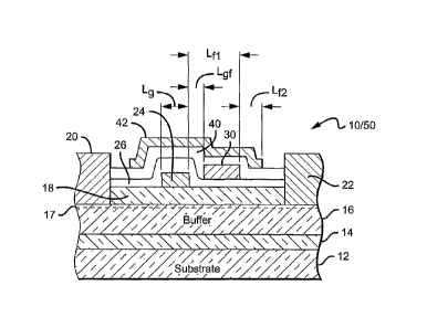
FIGs. 1 and 2 show one embodiment of a HEMT 10
according to the present invention that is preferably
Group-III nitride based although other material systems
can also be used. The HEMT 10 comprises a substrate 12
which can be made from silicon carbide, sapphire, spinet,
ZnO, silicon, gallium nitride, aluminum nitride, or any
other material or combinations of materials capable of
supporting growth of a Group-III nitride material. A
CA 02566361 2012-08-07
9
nucleation layer 14 can be formed on the substrate 12 to
reduce the lattice mismatch between the substrate 12 and
the next layer in the HEMT 10. The nucleation layer 14
should be approximately 1000 angstroms (A) thick,
although other thicknesses can be used. The nucleation
layer 14 can comprise many different materials, with a
suitable material being AlzGai_zN (0<=z<=1), and layer 14
can be formed on the substrate 12 using known
semiconductor growth techniques such as Metal Oxide
Chemical Vapor Deposition (MOCVD), Hydride Vapor Phase
Epitaxy (HVPE), or Molecular Beam Epitaxy (MBE).
The formation of a nucleation layer 14 can depend on
the material used for the substrate 12. For example,
methods of forming a nucleation layer 14 on various
substrates are taught in U.S. Patents 5,290,393 and
5,686,738. Methods of forming nucleation layers on
silicon carbide substrates are disclosed in U.S. Patents
5,393,993, 5,523,589, and 5,739,554.
The HEMT 10 further comprises a high resistivity
buffer layer 16 formed on the nucleation layer 14. The
buffer layer 16 can comprise doped or undoped layers of
Group III-nitride materials with a preferred buffer layer
16 made of a Group III-nitride material such as Al,GayIn(i-
x_y)N (0<=x<=1, 0<=y<=1, x+y<=1). Other materials can also
be used for the buffer layer 16 such as GaN that is
approximately 2pm thick, with part of the buffer layer
doped with Fe.
A barrier layer 18 is formed on the buffer layer 16
such that the buffer layer 16 is sandwiched between the
barrier layer 18 and the nucleation layer 14. Like the
CA 02566361 2012-08-07
buffer layer 16, the barrier layer 18 can comprise doped
or undoped layers of Group III-nitride materials.
Exemplary HEMT structures are illustrated in U.S. Patent
Nos. 6,316,793, 6,586,781, 6,548,333 and U.S. Published
5 Patent Application Nos. 2002/0167023 and 2003/00020092.
Other nitride based HEMT structures are illustrated in
U.S. Patents 5,192,987 and 5,296,395. The buffer and
barrier layers 16, 18 can be made using the same methods
used to grow the nucleation layer 14. Electric isolation
10 between the devices is done with mesa etch or ion
implementation outside the active HEMT.
Metal source and drain electrodes 20, 22 are formed
making ohmic contact through the barrier layer 18, and a
gate 24 is formed on the barrier layer 18 between the
source and drain electrodes 20, 22. Electric current can
flow between the source and drain electrodes 20, 22
through a 2DEG 17 induced at the heterointerface between
the buffer layer 16 and the barrier layer 18 when the
gate 24 is biased at the appropriate level. The formation
of source and drain electrodes 20, 22 is described in
detail in the patents and publications referenced above.
The source and drain electrodes 20, 22 can be made
of different materials including but not limited to
alloys of titanium, aluminum, gold or nickel. The gate 24
can also be made of different materials including but not
limited to gold, nickel, platinum, titanium, chromium,
alloys of titanium and tungsten, or platinum suicide.
The gate 24 can have many different lengths (Lig), with a
suitable gate length being to the range of 0.1 to 2
microns, although other gate lengths can be used. In one
CA 02566361 2006-11-08
W02005/114743 PCT/US2005/012821
11
embodiment according to the present invention a preferred
gate length (Lg) is approximately 0.5 microns.
A first non-conducting spacer layer 26 can be formed
at least over a portion of the surface of the barrier
layer between the gate and drain electrode, with a
preferred first spacer layer formed over the gate 24 and
the surface of the barrier layer 18 between the gate 24
and the source and drain electrodes 20, 22. The first
spacer layer 26 can comprise a dielectric layer, or a
combination of multiple dielectric layers. Different
dielectric materials can be used such as a SiN, Si02, Si,
Ge, Mg0x, MgNx, ZnO, SiNx, SiOx, alloys or 'layer
sequences thereof. The spacer layer can be many different
thicknesses, with a suitable range of thicknesses being .
approximately 0.05 to 2 microns. As best shown in FIG. 1,
the gate 24 is contacted at a gate contact 28.
When the first spacer layer 26 is formed before
device metallization the spacer layer can comprise an
epitaxial material such as a Group III nitride material
having different Group III elements such as alloys of Al,
Ga, or In, with a suitable spacer layer material being
AlxGai_xN (0x1). After epitaxial growth of the barrier
layer 18, the first spacer layer 26 can be grown using
the same epitaxial growth method. The first spacer layer
26 is then etched such that the gate 24, source electrode
20 and drain electrode 22 can be properly formed in
contact with the 2DEG 17. This arrangement is
particularly applicable to HEMTs (and MESFETs) having a
gate with an integral first field plate as shown in FIG.
9 and described below.
A first field plate 30 is formed on the spacer layer
26 between the gate 24 and the drain contact 22, with the
field plate 30 being in close proximity to the gate 24
CA 02566361 2006-11-08
W02005/114743 PCT/US2005/012821
12
but not overlapping it. The spacer layer 26 is arranged
to provide isolation between the first field plate 30 and
the layers below. A space between the gate 24 and field
plate (L9f) remains and should be wide enough to further
isolate from the first field plate 30, while being small
enough to maximize the field effect provided by the first
field plate 30. If Lgf is too wide the field effect will
be reduced. In one embodiment according to the present
invention Lgf should be 0.4 microns or less, although
larger and smaller spaces can also be used.
The first field plate 30 can extend different
distances Lf1 over the barrier layer from the edge of the
gate 24 with ,a suitable range of distances being 0.1 to
1.0 micron, although other distances can also be used.
The field plate 30 can comprise many different conductive
materials with a suitable material being a metal
deposited using standard metallization methods. In one
embodiment according to the present invention the field
plate 30 comprises the same metal as the feature that it
is connected to as described below.
The first field plate 30 can be electrically
connected to either the source contact 20 or the gate 24.
FIG. 1 shows one embodiment according to the present
invention wherein the first field plate 30 is connected
to the source contact, with two alternative connection
structures being shown, although other connection
structures can also be used. First conductive buses 32
(shown in phantom) can be formed on the spacer layer 26
to extend between the first field plate 30 and the source
contact 20. Different numbers of buses 32 can be used
although the more buses 32 that are used, the greater the
unwanted capacitance that can be introduced by the buses.
The buses 32 should have a sufficient number so that
CA 02566361 2006-11-08
WO 2005/114743 PCT/US2005/012821
13
current effectively spreads from the source contact 20
into the first field plate 30, while covering as little
of the HEMTs active region as possible, with a suitable
number of buses 32 being two.
The first field plate 30 can also be electrically
connected to the source contact 20 through a first
conductive path 34 that runs outside of the active region
of the HEMT 10 and is connected to the source contact 20.
As shown in FIG. 1, the path 34 runs outside the active
area of the HEMT at the edge opposite the gate contact
28. In alternative embodiments according to the present
invention, the conductive path could run outside the
active area of the HEMT 10 on the side of the gate
contact 28, or the HEMT 10 could include two or more
conductive paths running on one or both sides of the HEMT
10.
FIG. 3 shows another embodiment of a HEMT 50
according to the present invention that is similar to the
HEMT 10 in FIG. 1 and has the same sectional view as
20. shown in FIG. 2. For the features same or similar
features for the HEMT 50 in FIG. 3 (and for the figures
that follow), the same reference numerals from FIGs. 1
and 2 will be used with the understanding that the
description of the features above applies equally to the
HEMT 50.
Referring to FIGs. 2 and 3, the HEMT 50 comprises a
substrate 12, nucleation layer 14, buffer layer 16, 2DEG
17, barrier layer 18, a source electrode 20, drain
electrode 22, gate 24, first spacer layer 26, gate
contact 28 and first field plate 30. However, instead of
the first field plate being connected to the source
electrode 20, it is connected to the gate 24 and FIG. 3
shows two alternative gate connection structures that can
CA 02566361 2006-11-08
W02005/114743 PCT/US2005/012821
14
be used according to the present invention, although
other connection structures can also be used. One
connection structure can be conductive paths in the form
of conductive vias 52 (shown in phantom), which can be
formed running from the first field plate 30 to the gate
24, through the first spacer layer 26. The vias 52
provide an electrical connection between the gate 24 and
first field plate 30. The vias 52 can be formed by first
forming holes in the first spacer layer 26, such as by
etching, and then filling the holes with a conductive
material either in a separate step or during formation of
the first field plate 30. The vias 52 can be arranged
periodically down the first field plate 30 to provide for
effective current spreading from the gate 24 to the field
plate 30. By connecting to the gate 24 the gate
conductance is increased, which can allow a greater
device width for each unit cell.
The first field plate 30 can also be connected to
the gate 24 by a second conductive path 54 (shown in FIG.
3) that runs outside of the active region of the HEMT 50.
The conductive path 54 can connect to the gate contact 28
or a portion of the gate 24 outside of the HEMTs active
region, such as the portion of the gate 24 opposite the
gate contact 28.
The HEMTs 10 and 50 also comprise a second non-
conducting spacer layer 40 (shown in FIG. 2) that is
formed over the first field plate 30 and at least a
portion of the top surface of HEMT between the first
field plate and the drain, with a preferred second spacer
layer 40 as shown covering the first field plate and
the exposed surface of the first spacer layer 26. The
second spacer layer 40 can be formed of the same material
CA 02566361 2006-11-08
WO 2005/114743 PCT/US2005/012821
or layer materials as the first spacer layer 26 and can
have a total thickness in the range of 0.05 to 2 microns.
For HEMTs 10 and 50 the second field plate 42 can
= then be deposited on the second spacer layer 40.
5 Different second field plates according to the present
invention can provide different coverage, with the second
field plate 42 as shown overlapping the gate 24. Another
portion extends from over the edge of the first field
plate 30 toward the drain electrode 22 a distance Lf2,
10 which can be in the range of 0.2 to 5 microns.
The second field plate 42 is connected to the source
electrode 20 and many different connecting structures can
be used. Second conductive buses 44 can be formed on the
second spacer layer 40 to extend between the second field
15 plate 42 and the source electrode 20. Different numbers
of buses 44 can be used so that current effectively
spreads from the source electrode 20 into the second
field plate 42, while not covering too much of the active
region such that unwanted capacitance is introduced. The
first field plate 30 can also be electrically connected
to the source electrode 20 through a third conductive
path (not shown) that runs outside of the active region
of the HEMTs 10 and 50 and is coupled to the source
electrode 20.
After deposition of the second field plate 42 and
its connection to the source electrode 20, the active
structure can be covered by a dielectric passivation
layer (not shown), such as silicon nitride. Methods of
forming the dielectric passivation layer are described in
detail in the patents and publications referenced above.
FIGs. 4 and 5 show another embodiment of a HEMT 60
according to the present invention having many features
that are similar to those in HEMT 10 and 50. HEMT 60
CA 02566361 2006-11-08
WO 2005/114743 PCT/US2005/012821
16
comprises a substrate 12, nucleation layer 14, buffer
layer 16, 2DEG 17, barrier layer 18, source electrode 20,
drain electrode 22, gate 24, spacer layer 26 and gate
contact 28. The HEMT 60 also comprises a first field
plate 62 that is formed on the spacer layer 26 primarily
between the gate 24 and the drain electrode 22, but also
overlapping a portion of the gate 24. For the HEMTs 10
and 50 in FIGs. 1-3, Lgf (best shown in FIG. 2) is
relatively small, which can present some difficulties
during fabrication. By having the field plate 62 overlap
the gate 24, the HEMT 60 can be fabricated without having
to meet the tolerances of Lgf. The overlapping section of
the field plate 62, however, can introduce additional
unwanted capacitance. In determining whether to use an
overlapping field plate or non-overlapping field plate,
the ease of manufacturing must be balanced with the
reduced capacitance. The HEMT 60 also comprises either
buses 64 or a conductive path 66 to electrically connect
the field plate 62 to the source electrode 20.
FIG. 6 shows another embodiment of a HEMT 70 that is
similar to the HEMT 50 shown in FIG. 4 and can have the
same sectional view as shown in FIG. 5. The field plate
62 in HEMT 70, however, is connected to the gate 24
either by gate vias (not shown) that run between the
filed plate 62 and the gate through the spacer layer 26
or by a second conductive path 72.
Similar to HEMTs 10 and 50 shown in FIGs. 1-3, HEMTs
60 and 70 also comprise a second non-conducting spacer
layer 63 and a second field plate 65. Second conductive
buses 58 or a third conductive path (not shown) can be
used to connect the second field plate 56 to the source
electrode 20.
CA 02566361 2006-11-08
WO 2005/114743 PCT/US2005/012821
17
Each of the HEMTs 10, 50, 60, 70 described above (as
well as the HEMTs and MESFETs described below) can also
comprise more than two spacer layers and field plates,
wherein the topmost field plate is connected to the
source and the intermediate field plates are connected to
the source or gate. For example, FIG. 5 shows a third
spacer layer 68 and third field plate 69 (shown in
phantom) wherein the third field 69 that can extend from
the edge of the second field plate 65 toward the drain
electrode 22 and is connected to the source electrode
24. The first and second field plates 62, 65 are
connected to the source electrode 20 or gate 24.
The structures of the present invention can also be
used in other types of transistors made of other material
systems. FIG. 7 shows one embodiment of a MESFET 80
according to the present invention that is silicon
carbide based. MESFET 80 comprises a silicon carbide
substrate 82 on which a silicon carbide buffer 84 and a
silicon carbide channel layer 86 are formed with the
buffer 84 sandwiched between the channel layer 86 and
substrate 82. Source and drain electrodes 88, 90 are
formed in contact with the channel layer 86 and a gate 92
is formed on the channel layer 86 between the source and
drain electrodes 88, 90.
A non-conducting spacer layer 94 is formed over the
gate 92 and the surface of the channel layer 86 between
the gate 92 and the source and drain electrodes 88, 90.
Similar to the spacer layer 26 described above and shown
in FIGs. 1-3, the spacer layer 94 can comprise a layer of
non-conducting material such as a dielectric, or a number
of different layers of non-conducting materials such as
different dielectrics.
CA 02566361 2006-11-08
W02005/114743 PCT/US2005/012821
18
A first field plate 96 is formed on the spacer layer
94 between the gate 92 and the drain contact 90, with the
field plate 96 arranged in a similar fashion to the field
plate 30 in FIGs. 1-3 and has a similar Lgf and Ln. The
field plate 96 can also be connected to either the source
contact 88 or the gate 90 using the same structure for
connecting field plate 30.
A second non-conducting spacer layer 98 is formed
over the gate 96 and first spacer layer 94 and is similar
to second spacer layer 40 described above and shown in
FIGs. 1-3. Similarly, a second field plate 100 is
provided on the second spacer layer 98 that is similar to
the second field plate 42 and is similarly connected to
the source electrode 88.
FIG. 8 shows another embodiment of a silicon carbide
MESFET 110 according to the present invention that has
similar features of the MESFET 80 including a substrate
82, buffer 84, channel layer 86, source electrode 88,
drain electrode 90, gate 92 and spacer layer 94. MESFET
110 also comprises a field plate 112 that overlaps the
gate 92 and provides an embodiment that is easier to
manufacture than a MESFET with a non-overlapping field
plate, but can introduce !additional capacitance. Field
plate 112 is arranged in similar manner as field plate 62
in FIGs. 3-5 and is similarly connected to the source
electrode 88 or the gate 90. MESFET 110 also comprises a
second spreader layer 98 and a second field plate 100
connected to the source electrode 88.
FIG. 9 shows another embodiment of a HEMT 120 that
is similar to the HEMT 10 in FIGs. 1 and 2 and comprises
a substrate 12, nucleation layer 14, buffer layer 16,
2DEG 17, barrier layer 18, source electrode 20, drain
electrode 22, and gate 24. HEMT 120 also comprises a
CA 02566361 2006-11-08
W02005/114743 PCT/US2005/012821
19
spacer layer 122, but unlike the spacer layers described
above, spacer layer 122 does not cover the gate 24. It
instead only covers the surface of the barrier layer 18
between the gate 24 and the source and drain contacts 20,
22. It is understood, however, that the spacer layer can
cover less than all of the surface layer, but should
cover at least part of the surface between the gate 24
and the drain electrode 22 with the coverage being
sufficient to support a field plate in isolation from the
barrier layer 18.
A field plate 124 can then be formed on the spacer
layer 122, with the field plate being integral with the
gate 24 such that the field plate 124 contacts the gate
24 down its length. The field plate 124 extends a
distance Lfi on the spacer layer 122 toward the drain
contact 22. In this arrangement, the spacer layer 122 can
be epitaxial as described above, wherein the spacer layer
is deposited on the barrier layer 18 and then etched such
that the source and drain electrodes 20, 22 and gate 24
can be deposited in contact with the barrier layer 18.
The field plate 124 can then be deposited on the spacer
layer 122 integral with the gate 24 or the field plate
124 can be deposited during the same step that the gate
24 is deposited.
It is understood that the integral field plate
arrangement of FIG. 9 can be used with other transistors
such as MESFETs. It is also understood that transistors
with this field plate arranged can also have more than
two spacer layers and field plates.
A second spacer layer 124 and second field plate 126
are also included, similar to second spacer layer 40 and
field plate 42 described above and shown in FIGs. 1-3. It
is understood HEMT 120 can comprise more than two field
CA 02566361 2006-11-08
W02005/114743 PCT/US2005/012821
plates with the intermediate field plates electrically
connected to the gate or source electrode and the top
field plate electrically connected to the source
electrode. It is also understood that this multiple field
5 plate arrangement can also be used with other transistors
made of different material systems, such as with MESFETs
made of SiC.
FIG. 10 shows a table 130 comparing the operating
characteristics of GaN based HEMTs with no field plate,
10 field plate connected to the gate, and a field plate
connected to the source electrode. The tests were
conducted on HEMTs having a gate length (Lg) of 0.5
microns, FP length (Lf) of the first field plate of 1.1
microns, and a device width (w) of 500 microns. The test
15 showed that devices having a field plate connected to the
source electrode exhibit improved maximum stable gain
(MSG) and reduced reverse transmission (S12).
The source connected field plate arrangement
according to the present invention can be used in many
20 different HEMTs beyond those described above. For
example, FIG. 11 shows another embodiment of a HEMT 140
according to the present invention that has many features
similar to those in HEMTs 10, 50, 60 described above,
including a substrate 12, nucleation layer 14, buffer
layer 16, 2DEG 17, barrier layer 18, source electrode 20,
and drain electrode 22. HEMT 140, however, has a gamma
(') shaped gate 142 that is particularly adapted to high
frequency operation. The gate length (Lg) is one of the
important device dimensions in determining the speed of
the device, and with higher frequency devices the gate
length is shorter. Shorter gate length can lead to high
resistance that can negatively impact high frequency
operation. T-gates are commonly used in high frequency
CA 02566361 2006-11-08
W02005/114743 PCT/US2005/012821
21
operation, but it can be difficult to achieve a well-
coupled placement of a field plate with a T-gate.
The gamma gate 142 provides for low gate resistance
and allows for controlled definition of the gate
footprint. A spacer layer 144 is included that covers the
gamma gate 142 and the surface of barrier layer 18
between the gamma gate 142 and the source and drain
electrodes 20, 22, although the spacer layer 144 can
cover less as described above. A space can remain between
the 4orizontal portion of the gamma gate 82 and the top
of the spacer layer 144. The HEMT 140 also includes a
first field plate 146 on the spacer layer 144 that
overlaps that gamma gate 142. The first field plate 146
is preferably deposited on the side of the gamma gate 142
not having a horizontal overhanging section. This
arrangement allows for tight placement and effective
coupling between the field plate 146 and the active
layers below it. In other gamma gate embodiments the
field plate can be similarly arranged to field plate 86,
but instead of overlapping the gate, there can be a space
between the edge of the gate and the field plate similar
to space ligf shown in FIG. 2 and described above.
The field plate 146 can be electrically connected to
the gate 24 or the source electrode 20 in many different
ways as described above. In the case where it is
connected to the source electrode 20, the space between
the lower surface of the horizontal section of the gate
142 and the spacer layer 144 can present difficulties in
providing a conductive path directly between the field
plate 146 and the source electrode 20. Instead, one or
more conductive paths can be included, between the field
plate 146 and the source electrode 20 that run outside
the active area of the HEMT 140. Alternatively, the gamma
=
CA 02566361 2006-11-08
WO 2005/114743
PCT/US2005/012821
22
gate 142 can be completely covered by the spacer layer
144 with the space under the gate's horizontal section
filled. Conductive paths can then run directly from the
field plate 146 to the source electrode over the spacer
layer 144. The field plate 146 can alternatively be
connected to the gate using vias or conductive paths as
described above.
The HEMT 140 also comprises a second spacer layer
148 and a second field plate 150 formed on it and
connected to the source electrode 20. As with the first
field plate 146, the space between the lower surface of
the horizontal section of the gate 142 and the spacer
layer 144 can present difficulties in providing a
conductive path directly between the field plate 146 and
the source electrode 20. One or more conductive paths can
be included that run outside the active area of the HEMT
140. Alternatively, the gamma gate 142 can be completely
covered by the first or second spacer layers 144, 148
with the space under the gate's horizontal section
filled. Conductive paths can then run directly from the
field plate 146 to the source electrode over the spacer
layer 144. The active structure can then be covered by a
dielectric passivation layer (not shown).
FIG. 12 shows still another HEMT 160 according to
the present invention that can also be arranged with
multiple field plates as shown and described above. HEMT
160 also comprises a substrate 12, nucleation layer 14,
buffer layer 16, 2DEG 17, barrier layer 18, source
electrode 20, and drain electrode 22. The gate 162,
however, is recessed in the barrier layer 18, and is
covered by a spacer layer 164. A field plate 166 is
arranged on the spacer layer 164 and is either connected
to the source electrode 20 or gate 162. A second spacer
CA 02566361 2006-11-08
W02005/114743
PCT/US2005/012821
23
layer 168 is included on over the first field plate 166
and first spacer layer 164, with a second field plate 170
included on the second spacer layer 168 and electrically
connected to the source electrode 20. The top surface can
then be covered by a passivation layer (not shown). As
shown, the bottom portion of the gate 162 is only
partially recessed and in other embodiments the bottom
surface of the gate can be fully recessed or different
portions of the gate can be recessed to different depths
in the barrier layer 18.
The gamma and recessed gate arrangement described
above in FIGs. 11 and 12 can be used with different
transistors such as MESFETs and each can comprise more
than two spacer layers and field plates. The top field
plate should be connected to the source electrode while
the intermediate field plates below can be connected to
the source electrode or the gate. For example, a
transistor according to the present invention can have
three field plates, with the top one connected to the
source electrode and the ones below connected to either
the source electrode or the gate.
The embodiments above provide wide bandgap
transistors with improved power at microwave and
millimeter wave frequencies. The transistors exhibit
simultaneous high gain, high power, and more stable
operation due to higher input-output isolation. The
structure could be extended to larger dimensions for high
voltage applications at lower frequencies.
Although the present invention has been described in
considerable detail with reference to certain preferred
configurations thereof, other versions are possible. The
field plate arrangement can be used in many different
devices. The field plates can also have many different
CA 02566361 2012-08-07
24
shapes and can be connected to the source contact in many
different ways. For example, the field plate can extend
from over the HEMT's active area such that the connection
is continuous between the field plate and source contact,
instead of through buses or conductive paths. This
arrangement can, however, introduce prohibitive
capacitance into the structure. Accordingly, the scope of
the claims should not be limited by the preferred
embodiments set forth in the examples, but should be
given the broadest interpretation consistent with the
description as a whole.