Note: Descriptions are shown in the official language in which they were submitted.
CA 02566491 2006-11-09
WO 2005/109628 PCT/CA2005/000798
File No.: SW-0024-0
A TUNEABLE CIRCUIT FOR CANCELING THIRD ORDER MODULATION
FIELD OF THE INVENTION
[0001] The invention relates generally to radio frequency (RF) circuitry. More
particularly, the invention relates to tuning out the third order
intermodulation distortion term
in transconductance circuitry in CMOS technology.
BACKGROUND OF THE INVENTION
[0002] Wireless devices have been in use for many years for enabling mobile
data
and communication. Such devices can include mobile phones and wireless enabled
personal
digital assistants (PDAs) for example. Figure 1 is a generic block diagram of
the core
components of such wireless devices. The wireless core 10 includes a baseband
processor
12 for controlling application specific functions of the wireless device and
for generating and
receiving voice or data signals to a radio frequency (RF) transceiver chip 14.
The RF
transceiver chip 14 is responsible for frequency up-conversion of transmission
signals, and
frequency down-conversion of received signals. The RF transceiver chip 14
includes a
receiver core 16 connected to an antenna 18 for receiving transmitted signals
from a base
station or another mobile device, and a transmitter core 20 for transmitting
signals through
the antenna 18 via a gain circuit 22. Those of skill in the art will
understand that Figure 1 is a
simplified block diagram, and can include other functional blocks that may be
necessary to
enable proper operation or functionality.
[0003] Third-order intermodulation (IM3) is a common interference problem in
RF
where two or more signals mix in a non-linear phase or "device" to form one or
more new
signals, and thereby creating intermodulation products. In the RX section of a
transceiver
chip, these intermodulation signals may fall on top of a desirable signal (in
frequency
domain) thereby reducing the signal to noise ratio. For the TX section,
intermodulation may
cause the signal to spread out causing power to leak in a neighbouring band.
Various
elements within a radio use transconductance cells. These transconductance
cells convert
voltage into current, but also add third order harmonic distortion. As an
example, active
mixers typical use transconductance cells as an input stage to the mixing cell
and are widely
used in modern communication systems in order to achieve frequency translation
of the
-1-
CA 02566491 2006-11-09
WO 2005/109628 PCT/CA2005/000798
File No.: SW-0024-0
carrier signals. Intermodulation distortion in the mixer affects the dynamic
range of most
communication systems. The IM3 of transconductance cells is governed by the
voltage to
current transfer function produced by elements within the cell (i.e.
transistors) and the
amount of feedback in the circuit
[0004] A typical output of a transconductance circuit is given by:
...
Zaut = - AlV in + A3 Vj3n +
where iout is the output current, A, is the transconductance gain of the
circuit, v;n is the input
voltage, and An are distortion terms where n>3. However, a nearly linear
relationship
between iout and v;n is desirable since many communications standards specify
the amount of
distortion that is acceptable. Failure to comply with such standards may
result in non-
certification of a device. It is therefore desirable to eliminate distortions.
[0005] In the past, distortion cancellation was accomplished by techniques
employing
bipolar transistors as shown in such references as US Patent No. 6,781,467
(Sun), US
Patent No. 5,497,123 (Main et al), S. Otaka, M. Ashida, M. Ishii, T. Lakura,
"A +10dBm IIP3
SiGe Mixer with Cancellation Technique," ISSCC2004, and B. Gilbert, "The
MICROMIXER: A
highly linear variant of the Gilbert mixer using a bisymmetric class-AB input
stage" in J. Solid-
State Circuits, vol. 32, pp. 1412-1423, Sept. 1997. The general approach of
linearization is
to add circuitry such that the terms An are brought to zero and A, remains
approximately the
same (in most cases A, reduces); note, for an ideal amplifier An = 0, where n
is greater than
or equal to 3. In Main et al and Otaka, A3 is made up of two terms that oppose
each other;
i.e.
A3 = A3 - A3
where A3+ and A3- are made equal using component values in the circuit. In
Main et al a
phase shifting technique is used and is applied to a mixer architecture. In
Otaka, a resistor
value is used set the A3 to zero. The linearization technique used by Gilbert
consists of pre-
distorting the signal so that the terms An are set to zero at the output after
it passes thru a
distorting amplifying stage, which will introduces excessive noise. Sun uses
bipolar transistor
technology for a low noise amplifier. All these methods reduce the amount of
third order
distortion, but these past implementations are bipolar based, opposed to
Complementary
Metal Oxide Semiconductor (CMOS) based. The advantages of CMOS technology are
cost
-2-
CA 02566491 2006-11-09
WO 2005/109628 PCT/CA2005/000798
File No.: SW-0024-0
and the fact the technology improves at a rate given by Moore's Law. These
techniques are
also susceptible to manufacturing variations in device parameters.
Specifically, the IM3 may
not be reduced because of variations in transistors parameters from part to
part. Other
techniques use feedback to reduce the amount of IM3 in a circuit. However
feedback circuits
introduce noise and increase the total amount of current and area required by
the circuit.
[0006] Such techniques also employ SiGe or GaAs devices and technology, which
although they exhibit highly linear characteristics, the technologies are new
and expensive.
Consequently, the cost of manufacturing often outweighs the benefits of using
such devices.
[0007] It is therefore desirable to provide CMOS technology for tuning out IM3
products in transconductance circuits. The invention described below is a
tuneable method
for reducing the IM3 tone in a transconductance element so to make it less
susceptible to
manufacturing variations and the transconductance implementation is described
within
CMOS technology.
SUMMARY OF THE INVENTION
[0008] It is therefore an object of the invention to obviate or mitigate at
least one
disadvantage of previous IM3 cancellation circuits. More specifically, it is
an object of the
invention to provide a system for a providing a transconductor for tuning IM3
component out
of CMOS circuitry.
[0009] In a first aspect, the invention provides a CMOS transconductor for
cancelling
third-order intermodulation of an output current corresponding to an input
voltage. The
transconductor includes a transconductance circuit and a tuneable distortion
circuit. The
transconductance circuit takes an input voltage and generates an output
current having a
transconductance element and an IM3 element. The distortion circuit takes the
same input
voltage and generates a current having an IM3 element of equal amplitude and
opposite
phase to the IM3 element of the differential circuit. A controller circuit
tunes the distortion
circuit to adjust its IM3 element to substantially equal the amplitude of the
IM3 of the
differential circuit. The distortion and differential circuits are arranged to
sum their output
currents thereby effectively cancelling the IM3 elements, leaving the
transconductance
relatively unmodified.
-3-
CA 02566491 2006-11-09
WO 2005/109628 PCT/CA2005/000798
File No.: SW-0024-0
[0010] In a further embodiment of the invention, the transconductance cell is
a
differential pair of transistors, and the distortion circuit is a differential
pair of transistors
having a resistor tuneable by a control circuit. The control circuit may use
digitai logic to
switch in different said resistor values. The differential and distortion
circuits may be biased
independently at the respective inputs by a resistor and decoupling capacitors
to the input of
transconductance cell and the distortion circuit.
[0011] In a second aspect of the invention, a CMOS mixer is provided having a
transconductance circuit and a distortion circuit tuneable by a controller
circuit coupled to
switching circuit for switching the output current of the summed currents of
the differential
and distortion circuits. The switched output current is converted to an output
voltage by a
resistive active load coupled to the switching circuit.
[0012] In a third aspect of the invention a CMOS amplifier is provided having
a
differential circuit and a distortion circuit tuneable by a controller circuit
coupled to active
resistive elements for converting said output current to an output voltage.
[0013] Other aspects and features of the invention will become apparent to
those
ordinarily skilled in the art upori review of the following description of
specific embodiments of
the invention in conjunction with the accompanying figures.
BRIEF DESCRIPTION OF THE DRAWINGS
[0014] Embodiments of the invention will now be described, by way of example
only,
with reference to the attached Figures, wherein:
Fig. I is a block diagram of the core components of a wireless device;
Fig. 2 is a block diagram of a transconductor for cancelling third-order
intermodulation;
Fig. 3 is a circuit of a transconductor for cancelling third-order
intermodulation;
Fig. 4 is a plot of the difference in third-order modulation elements versus
resistance of a tuning element;
Fig. 5 is a circuit of a transconductor for cancelling third-order
intermodulation
using a current source;
Fig. 6 is a circuit of a transconductor for cancelling third-order
intermodulation
showing the main transconductance cell and the distortion cell with a DC
biased;
-4-
CA 02566491 2006-11-09
WO 2005/109628 PCT/CA2005/000798
File No.: SW-0024-0
Fig. 7 is a circuit of a mixer using the transconductor for cancelling third-
order
intermodulation; and
Fig. 8 is a circuit of an amplifier using the transconductor for cancelling
third-
order intermodulation.
DETAILED DESCRIPTION
[0015] Generally, the invention provides a system for cancelling third-order
intermodulation in CMOS RF circuitry. In particular, a transconductance
circuit produces an
output current as a function of an input voltage, having a transconductance
and a third order
intermodulation, which is cancelled by the output current of a tuneable
distortion circuit
coupled to the differential circuit while the transconductance is
comparatively unchanged.
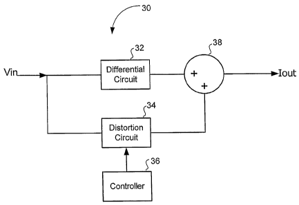
[0016] Figure 2 shows a block diagram of a transconductor for cancelling third-
order
intermodulation. The transconductor 30 can be used in any of the blocks in
Figure 1. The
transconductor 30 has a main transconductance circuit 32, a tuneable
distortion circuit 34
and a controller circuit 36. The differential circuit 32 generates an output
current having a
transconductance gain component and an IM3 component, based on the input
voltage, V;,
The distortion circuit 34 generates an output current of opposite phase to the
output current
of the main transconductance circuit output current and minimal
transconductance
comparatively. The IM3 of the distortion circuit current is tuned by the
controller circuit 36 to
match the amplitude of the IM3 of the transconductance circuit. The currents
are summed in
38 so that the IM3 components substantially cancel out and the
transconductance gain
component remain substantially unchanged.
[0017] The transconductance circuit 32 is a differential set of transistors.
The
operation of a differential set of transistors is well known in the art. In an
example of a
transconductor 40 as described in Figure 2, Figure 3 shows the differential
set of transistors
to be MOSFETs 42, 44, having differential inputs at the gate, and grounded at
the source.
The distortion circuit 34 in this example is also a pair of MOSFETs 46, 48
with the sources
connected to a resistor 50 or set of switchable resistors that goes to ground
and is
controllable by a control circuit (not shown). The distortion MOSFETs 46, 48,
and the resistor
50 produce an IM3 being a function of the resistor value. The distortion
MOSFETs are
-5-
CA 02566491 2006-11-09
WO 2005/109628 PCT/CA2005/000798
File No.: SW-0024-0
designed to have a minimal transconductance element. When summed together at
the
outputs 52, 54, the currents from the distortion circuit and the differential
circuit substantial
cancel out depending on the value of the variable resistor. The control
circuitry may
preferably consist of digital switches and analog switches to change the
resistor value. The
resistor values may change in a continuous manner or in a- discrete manner.
The control
circuitry may also change the resistor value in an analog sense; that is, the
resistor element
50 is made up of active elements.
[0018] The plot in Figure 4 shows the relationship between the resistance of
the
tuneable distortion circuit and IM3 as measured at the differential output. As
resistance
changes the difference between the two IM3 components change and an optimal
resistance
is found when the difference between the two IM3 components is zero.
[0019] Figure 5 shows a circuit of a transconductor 40 for cancelling third-
order
intermodulation using a current source 60 as opposed to a resistor 50 as shown
in Figure 3.
In this example, a tuning current source having It,ne is used to nullify the
IM3. The current Itune
controls the amount of IM3 component generated by the distortion circuit 34.
[0020] Figure 6 shows the differential circuit and the distortion circuit of
the
transconductor being independently biased by decoupling capacitors 72, 74 and
76, 78.
Decoupling capacitors are placed between the two input pairs. Biasing voltages
Vbl, Vb2 are
applied to the loads 80, 82, which are used to isolate the signal from the
biasing voltages.
Such biasing may be used to aid in the reduction of IM3 products. In this
example, resistor
50 may be replaced with a current source 60 as shown in Figure 5. In this
figure, the IM3 is
either controlled by the resistor 50, Vb2, or both.
[0021] An example of how the transconductor may be used in an application is
shown in Figure 7 where the circuit 90 has a transconductor 40, which is
coupled to a
switching circuit 92 to create a mixer circuit. The transconductance current
produced by the
MOSFETs 42, 44, 46, 48 of the transconductor 40 is switched by the local
oscillator LO
signals 102, 104, 106 (or from a signal that is generated from a local
oscillator) and
converted into an output voltage by the RL active loads 108, 110. The FETs 94,
96, 98, and
100 make up a mixing switching quad which is well known in the art today. The
output Vout
112, 114 is either a down or up converted signal of Vin in the frequency
domain. In this
-6-
CA 02566491 2006-11-09
WO 2005/109628 PCT/CA2005/000798
File No.: SW-0024-0
application, the transconductor 40 may use a current source in place of the
tuneable resistor
50. The transconductor in this example may also be biased according to Figure
6.
[0022] Another example of a use of the transconductor circuit is shown in
Figure 8
where the transconductor is used in an amplifier circuit 120. Here the active
loads 122, 124
convert the output current of the transconductor into a voltage Vout at the
output 126.
[0023] The above-described embodiments of the invention are intended as
examples
only. Alterations, modifications and variations may be effected to the
particular embodiments
by those of skill in the art without departing from the scope of the
invention, which is defined
solely by the claims appended hereto.
-7_